分立半导体
子分类
产品(1814)

TPD4E05U06DQAR - 4-Ch 0.5pF ESD TVS Diode | TI
The Texas Instruments TPD4E05U06DQAR is a quad-channel unidirectional TVS-based ESD protection diode array with ultra-low 0.5 pF channel capacitance, 5.5 V reverse standoff voltage, and IEC 61000-4-2 ESD protection up to ±12 kV, housed in a 10-pin USON (2.5 mm x 1 mm) surface-mount package. An ESD protection device, also called a transient voltage suppressor (TVS) array or surge protector, is a circuit-protection component that diverts fast electrostatic discharge and cable-discharge events away from sensitive high-speed ICs. In the system hierarchy it sits in the circuit protection layer of board-level electronics, ahead of transceivers, serializers, and PHY devices that would otherwise suffer latent or catastrophic ESD damage. Key features include four protection channels for high-speed differential pairs, an exceptionally low 0.5 pF off-state loading capacitance that preserves signal integrity on 6 Gbps links, a low clamping voltage of 14 V during ESD events, and a 2.5 A (8/20 us) peak pulse current rating. The device dissipates ESD strikes exceeding the maximum level specified by the IEC 61000-4-2 international standard, per the TI TPDxE05U06 datasheet. Technically, the TPDxE05U06 family uses unidirectional TVS diode structures steering ESD transients from protected I/O lines to ground. The ultra-low loading capacitance is the defining parameter: at USB 3.0, HDMI, and eSATA data rates, even 1 pF per channel can degrade eye diagrams, so 0.5 pF loading preserves impedance matching and minimizes jitter on 5-6 Gbps super-speed lanes. Typical applications include USB 3.0/3.1 port protection, HDMI connector protection, Ethernet and DisplayPort interfaces in consumer electronics and connectivity equipment, and general high-speed data-line ESD protection in docking stations, smartphones, tablets, and industrial controllers. A key design consideration is placement: locate the device within a few millimeters of the connector so the ESD current path to ground is as short as possible, and keep the ground return low-impedance with vias directly to the ground plane. This page synthesizes distributor pricing, drop-in alternatives, practical design notes, and AEO-optimized FAQs not found in the manufacturer datasheet alone.

TPD4E1U06DBVR - Quad 0.8pF ESD Protection TVS | Texas Instruments
The Texas Instruments TPD4E1U06DBVR is a quad-channel unidirectional TVS-based ESD protection diode with ultra-low 0.8 pF line capacitance, a 5.5 V working voltage, and ±15 kV ESD strike immunity per IEC 61000-4-2, housed in a 6-pin SOT-23 (DBV) surface-mount package. An ESD protection diode array (also called a TVS diode array or transient voltage suppressor) is a circuit-protection component that diverts fast electrostatic discharge and cable-discharge transients away from sensitive silicon before damage occurs. Within the system hierarchy, it sits at the board level under surge protection and circuit protection, guarding high-speed interface lines such as USB, HDMI, and audio connectors. Key features include the 0.8 pF ultra-low channel capacitance, which minimizes signal-integrity degradation on multi-hundred-Mbps high-speed lines; the 5.5 V reverse standoff voltage, which covers 5 V and 3.3 V rails; and a 15 V typical clamping voltage with 3 A (8/20 us) peak pulse current capability. According to the TI product data, the device can dissipate ESD strikes above the maximum level specified by the IEC 61000-4-2 international standard. The unidirectional steering-diode architecture routes positive transients to a common ground reference, keeping residual voltage at the protected IC low during a strike. The four independent channels let one small SOT-23-6 package protect an entire 4-line differential or single-ended interface, reducing BOM count and board area compared with discrete diodes. Typical applications include USB 2.0 port protection, HDMI and display-interface line protection, and analog audio jack ESD suppression - all environments where connector-mediated human contact demands robust ESD ratings and where sub-1-pF capacitance preserves eye diagrams and audio fidelity. Design consideration: place the TPD4E1U06DBVR as close to the connector as possible, before any series resistors or common-mode chokes, so the transient is clamped at the point of entry; every millimeter of trace between the connector and the diode adds inductance that worsens residual clamping voltage. This page synthesizes verified distributor data, drop-in alternatives, comparison tables, and practical layout design notes not found together in the manufacturer datasheet.

TPD4E1U06DCKR - 0.8pF Quad ESD Protection TVS | Texas Instruments
The Texas Instruments TPD4E1U06DCKR is a quad-channel unidirectional ESD protection TVS diode array with ultra-low 0.8 pF line capacitance, a 5.5 V working voltage, ±15 kV ESD protection per IEC 61000-4-2, and a typical 15 V clamp voltage with 3 A (8/20 us) Ipp capability, housed in a 6-pin SC-70 (SOT-363/SC70-6) surface-mount package. An ESD protection device is a type of transient voltage suppressor (TVS) that clamps electrostatic discharge and cable-discharge events before they reach sensitive IC pins. Within the power and signal integrity hierarchy, it sits under circuit protection -> TVS diode -> ESD protection array, complementing port controllers and transceivers. Because modern high-speed interfaces carry data at hundreds of Mbps to multiple Gbps, protection devices must add minimal capacitive loading; a low-capacitance array like this one preserves signal eye diagrams on USB, HDMI, and LVDS lines. Key differentiating features include the 0.8-pF per-channel line capacitance, the quad-channel integration that protects four lines in a single 2.0 mm x 1.25 mm footprint, IEC 61000-4-2 level performance of ±15 kV air gap and ±8 kV contact discharge, and a unidirectional clamp structure suited to single-ended data and power lines. The 5.5 V reverse standoff voltage makes it usable on 5 V and 3.3 V rails as well as low-voltage data lines. Architecturally, each channel is a forward-biased silicon avalanche diode arrangement that steers surge current to ground with fast response, dissipating ESD strikes above the maximum level specified by the IEC 61000-4-2 international standard. The ultra-low junction capacitance is achieved through TI's small-geometry diode process, minimizing insertion loss at high data rates. Typical applications include USB 2.0 and USB 3.x port protection, high-speed digital data lines in portable electronics, and industrial communication interfaces such as RS-485 or Ethernet aux lines. Any interface with 1-4 exposed lines and a 5.5 V or lower supply benefits. Design consideration: keep the TPD4E1U06 close to the connector with a short, low-inductance ground return; ground lead inductance dominates residual clamp voltage during an 8/20 us surge. This page synthesizes distributor pricing, drop-in alternatives including the TPD4E1B06DCKR and TPD4S009DCKR, and practical design notes not found in the manufacturer datasheet.
TPD4S009DBVRG4 - 4ch 0.8pF ±8kV ESD TVS Array | TI
The Texas Instruments TPD4S009DBVRG4 is a four-channel TVS diode array for ESD protection of high-speed differential interfaces, rated for ±8-kV contact discharge per IEC 61000-4-2 Level 4, with only 0.8-pF line capacitance and a 5.5-V operating voltage, housed in a 6-pin SOT-23 (DBV) surface-mount package. An ESD protection diode array, also called a TVS (transient voltage suppressor) array, is a circuit-protection component that clamps electrostatic-discharge and cable-discharge events before they reach sensitive transceiver silicon. Within the protection hierarchy, it sits at board level between the external connector and the protected IC, downstream of system-level surge arrestors and upstream of the chip's internal ESD structures, which it offloads. Key features include the 0.8-pF ultra-low channel capacitance that preserves high-speed signal integrity on differential pairs, ±8-kV IEC 61000-4-2 contact and ±15-kV-class air-gap robustness per the device family rating, and an integrated VCC pin that lets the array clamp against the supply rail for bidirectional line protection. Excellent channel-to-channel matching keeps skew on differential pairs minimal, and the flow-through pinout simplifies routing from connector to transceiver. The device uses a clamp-type TVS architecture with low dynamic resistance, so clamping voltage during an 8-kV contact strike stays low enough to protect typical high-speed transceivers. According to the TI datasheet, the TPD4S009 family is specifically characterized for high-speed differential interfaces where capacitance and symmetry dominate signal-eye performance. Typical applications include HDMI and DisplayPort port protection, USB differential-line ESD clamping, and general high-speed interface protection in consumer electronics and connectivity equipment. The four-channel arrangement protects a full differential pair pair, or several single-ended lines, in one small package. Design consideration: keep the array within millimeters of the connector and route symmetrically through the device; series inductance before the TVS dominates clamp performance more than the diode specification itself. This page synthesizes verified distributor listings, drop-in alternative analysis, and practical design notes not found in the manufacturer datasheet.
TPD4S009DCKRG4 - Quad 0.8pF 5.5V ESD Protection | TI
The Texas Instruments TPD4S009DCKRG4 is a quad-channel ESD protection diode array for high-speed differential interfaces, featuring 0.8 pF line capacitance, 5.5 V working voltage, and ±8 kV contact-discharge ESD protection per IEC 61000-4-2 Level 4, housed in a 6-pin SC-70 (SOT-363, DCK) package. An ESD protection TVS (transient voltage suppressor) diode array is a type of circuit-protection semiconductor that clamps electrostatic-discharge and cable-discharge events before they reach sensitive transceiver silicon. Within the protection hierarchy, it sits alongside TVS diodes and surge protectors, serving as the first line of defense in power management and interface circuits. Key features include an ultra-low 0.8 pF typical line capacitance, which preserves signal integrity on differential pairs running at multi-hundred-megabit rates; excellent channel-to-channel capacitance matching, which minimizes skew between the two legs of a differential pair; and a dedicated VCC pin that lowers clamping voltage during ESD strikes on powered systems. The device is rated for ±8 kV IEC 61000-4-2 contact discharge, the maximum Level 4 severity. Architecturally, the four steering/clamping diodes route ESD current from any I/O line to the VCC rail and ground, so transient energy is shared across the array rather than concentrated at one junction. The low junction capacitance is achieved without sacrificing robust clamping, and the SC-70-6 footprint keeps parasitic inductance low — critical because even a few nanohenries of trace inductance raises the effective clamping voltage during a fast ESD edge. Typical applications include HDMI, Display Port, and LVDS display-port ESD protection, USB and Ethernet differential-line protection, and ESD protection for high-speed digital interfaces in consumer, industrial, and networking equipment. Design-wise, keep the device close to the connector and use short, direct traces to the protected lines; place a bulk capacitor near VCC to absorb diverted charge. This page synthesizes distributor availability, drop-in alternatives, comparison tables, and practical design notes not found in the manufacturer datasheet.
TPD4S012DRYR - 4-Ch USB ESD Protection, 15V VBUS | TI
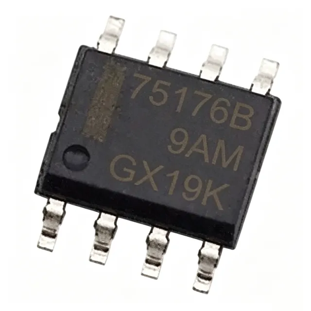
The Texas Instruments TPD4S012DRYR is a 4-channel transient voltage suppressor (TVS) ESD protection diode array purpose-built for USB High-Speed (HS), USB On-The-Go (OTG), and USB charger interfaces. It integrates four 0.8-pF low-capacitance protection channels plus a power-rail clamp with 15-V tolerance on the VBUS line, in an ultra-small flow-through 6-SON (1.45 mm x 1 mm) package rated for IEC 61000-4-2 system-level ESD strikes of ±10 kV (contact/air). An ESD protection diode array is a type of transient voltage suppressor (TVS) within the broader circuit-protection hierarchy: surge protector -> TVS diode -> ESD protection array. Its role is to clamp fast electrostatic-discharge transients before they reach sensitive transceiver silicon, diverting charge to ground or to the supply rail while remaining invisible to the high-speed signal during normal operation. Key differentiating features include: (1) 0.8 pF typical line capacitance, which preserves USB 2.0 high-speed eye diagrams at 480 Mbps with minimal insertion loss; (2) 15-V VBUS tolerance, allowing the power clamp to survive charger voltages and OTG VBUS events that would destroy ordinary 5.5-V clamps on data lines; (3) 3-A (8/20 us) Ipp clamp capability on the power path; and (4) a flow-through package that enables clean differential D+/D- routing without stubs. The device uses snapback-free directional TVS cells on D+/D- and a dedicated zener-based clamp for VBUS, achieving sub-nanosecond response to ESD events per IEC 61000-4-2 testing. Typical applications are smartphone and tablet USB ports, portable charger power paths, USB OTG connectors, and any downstream USB transceiver exposed to user-handled connectors. Design consideration: keep the TPD4S012 within a few millimeters of the connector and place the ground connection to a low-impedance plane; ESD protection effectiveness degrades rapidly with trace inductance. Prices as of 2026-08-29.
TPD4S012DRYR - 4-Ch USB ESD Protection, 15V VBUS | TI
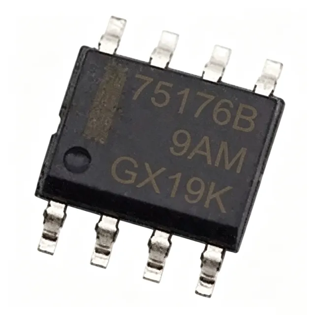
The Texas Instruments TPD4S012DRYR is a 4-channel transient voltage suppressor (TVS) based ESD protection diode array with 0.8-pF line capacitance, ±10-kV IEC 61000-4-2 system-level ESD protection, and 15-V VBUS tolerance, housed in a 6-SON (1.45 mm x 1 mm) surface-mount package. An ESD protection diode array is a specialized category of transient voltage suppressor within the broader circuit-protection hierarchy: surge protector -> TVS diode -> ESD protection array. Its function is to clamp nanosecond-scale electrostatic discharge transients at a connector before they reach sensitive transceiver silicon, diverting charge to ground or the supply rail while remaining electrically invisible to the high-speed signal during normal operation. Key differentiating features include 0.8 pF typical channel capacitance, which preserves USB 2.0 high-speed (480 Mbps) eye diagrams with minimal insertion loss; a dedicated power clamp with 15-V tolerance on the VBUS line, allowing it to survive charger overvoltages and OTG VBUS events that would destroy ordinary 5.5-V data-line clamps; and a 3-A (8/20 us) Ipp clamp capability on the power path. Architecturally, the device combines snapback-free directional TVS cells on D+/D- and ID lines with a zener-based clamp for VBUS, achieving sub-nanosecond response to ESD events per IEC 61000-4-2 testing. The flow-through pinout enables clean differential D+/D- routing without stubs, protecting 3 high-speed I/O lines plus VBUS simultaneously - a combination specifically targeted at USB OTG designs. Typical applications include smartphone and tablet USB ports, portable charger power paths, USB OTG connectors on media players and cameras, and any downstream USB transceiver exposed to user-handled connectors. Design consideration: place the TPD4S012 within a few millimeters of the connector and return its ground pin to a low-impedance plane; protection effectiveness degrades rapidly with added trace inductance. This page synthesizes distributor availability, drop-in alternative analysis, and practical layout guidance not found in the manufacturer datasheet. Pricing shown is estimated as of 2026-09-01.
TVS4201MR6T1G - 5V TVS Array, 12V Clamp, 6-TSOP | onsemi
The onsemi TVS4201MR6T1G is a low-capacitance transient voltage suppressor (TVS) diode array designed to protect high-speed data lines from ESD, EFT, and lightning-induced surges. Housed in a compact 6-pin TSOP-6 (TSOT-23-6) surface-mount package, it integrates a unidirectional 5 V working-voltage TVS array that clamps at 12 V and absorbs up to 25 A of peak pulse current (8/20 µs waveform), making it a drop-in protection block for USB, HDMI, and other consumer interface ports. A TVS (transient voltage suppressor) diode is a specialized clamping device that maintains a near-open circuit under normal operating conditions but rapidly conducts (clamps) when the line voltage exceeds its breakdown threshold, shunting dangerous transients to ground before downstream ICs can be harmed. The TVS4201MR6 family is part of onsemi's low-capacitance portfolio, optimized for high-speed lines where excessive loading capacitance would otherwise degrade signal integrity. Key features include 12 V maximum clamping voltage at 25 A (8/20 µs), 5 V reverse working voltage (Vrwm), an integrated unidirectional TVS array, low line-to-line capacitance suited to high-speed data rates, and an operating temperature range of -40 °C to +125 °C. The 6-TSOP package also meets AEC-Q101 automotive qualification criteria, enabling deployment in body-electronics and infotainment designs alongside consumer applications. The TVS4201MR6T1G uses onsemi's TVS array process that integrates steering diodes in a compact form factor, achieving tight clamping behavior with minimal series inductance. This architecture is purpose-built for transient suppression on differential or single-ended lines where a small PCB footprint and high surge-handling are simultaneously required, reducing the BOM count compared to discrete TVS solutions. Typical applications include USB 2.0/3.0 data-line clamping, HDMI/MHL/MIPI video-interface protection, smartphone charging-port ESD protection, automotive infotainment and body-control ports, and general-purpose I/O protection on microcontroller or SoC pins. Designers favor this part because it provides datasheet-verified surge and ESD immunity in a footprint compatible with industry-standard TSOT-23-6 TVS arrays. For best results, place the TVS as close as possible to the connector and use a low-inductance ground return via multiple vias. Ensure that the trace between the protected IC and the connector is short and direct, with the TVS ground stitch tied to the chassis or system ground rather than the digital ground, to maximize surge dissipation and minimize residual clamping voltage seen by the protected IC. This page synthesizes distributor pricing, AEC-Q101 automotive-grade drop-in alternatives in the same 6-TSOP footprint, and practical PCB-layout design notes not found in the onsemi datasheet, providing engineering value beyond raw specification repetition.

UF3007 - 3A 800V Ultra-Fast Rectifier Diode | Diodes Inc
The Diodes Incorporated UF3007 is a 3.0 A ultra-fast rectifier diode with an 800 V repetitive peak reverse voltage, a 1.7 V maximum forward voltage drop, and a 75 ns reverse recovery time, housed in a DO-201AD (DO-27 style) axial-lead through-hole package. An ultra-fast rectifier is a power semiconductor diode engineered for very short reverse recovery time (trr), which is the interval during which the diode continues to conduct after the applied voltage reverses. Within the power-conversion component hierarchy, the ultra-fast rectifier is a member of the rectifier diode family, which in turn belongs to discrete semiconductors and power management building blocks. Fast recovery matters because slow diodes dissipate significant switching losses in high-frequency converters. Key features of the UF3007 include a diffused-junction construction optimized for high switching efficiency, a surge overload rating of up to 150 A peak (non-repetitive), low reverse leakage current, and a plastic body carrying a UL flammability classification of 94V-0. High current capability combined with low forward voltage drop reduces conduction losses in the output stage. Technical analysis: the 75 ns trr class places the UF3007 well below standard-recovery diodes (microseconds) and suits switching frequencies commonly found in flyback and forward converters. According to the manufacturer datasheet, for capacitive loads the output current should be derated by 20% relative to the resistive-load rating. Storage temperature spans -65C to +175C per typical DO-201AD ratings, enabling rugged industrial designs. Typical applications include secondary-side output rectification in AC-DC switch-mode power supplies, free-wheeling and snubber circuits in motor drives, DC-DC converter output stages, and reverse-polarity protection in industrial equipment. Design consideration: keep lead length short and verify average forward current derating at elevated ambient temperatures, since DO-201AD axial packages rely on lead conduction for heat extraction. This page synthesizes distributor cross-reference data, drop-in alternatives, and practical design notes not found in the manufacturer datasheet alone.

ULC0502P3 - 5V 2-Line Ultra-Low Capacitance TVS | Leiditech
The Shanghai Leiditech Electronic Technology ULC0502P3 is a 2-line ultra-low capacitance transient voltage suppressor (TVS) diode array rated for 5V operating voltage, housed in a 3-pin leadless DFN1006-3 (1.0mm x 0.6mm x 0.5mm) package. It is engineered to protect two high-speed data lines or signal lines from electrostatic discharge (ESD), electrical fast transients (EFT), and lightning-induced surges, while adding minimal parasitic loading to the protected lines. A TVS (Transient Voltage Suppressor) diode is a solid-state semiconductor device designed to clamp voltage spikes and divert transient currents away from sensitive downstream ICs. Within the protection hierarchy (TVS diode -> ESD suppressor -> surge protector -> circuit protection component), TVS diodes sit at the IC-port level and are routinely placed next to USB, HDMI, MIPI, and antenna connectors. Ultra-low capacitance variants like the ULC0502P3 specifically target high-speed signal lines where conventional TVS diodes would degrade signal integrity. Key features of the ULC0502P3 include ultra-low leakage at the nA level, a low 5V operating (working) voltage, low clamping voltage during transient events, and a miniature 3-pin leadless DFN1006-3 footprint. The device is compliant with IEC 61000-4-2 ESD immunity testing at +/-30kV air discharge and +/-25kV contact discharge, with IEC 61000-4-4 EFT immunity at 40A (5/50ns) and IEC 61000-4-5 surge immunity at 5A (8/20us). Lead finish is NiPdAu (nickel-palladium-gold) for reliable soldering and corrosion resistance, and the device is RoHS compliant. The ULC0502P3 is best understood as a two-channel unidirectional low-capacitance ESD diode in a sub-millimeter package, optimized for high-speed signal routing. Compared with general-purpose TVS diodes that may add tens of picofarads of junction capacitance, ultra-low capacitance parts such as this one preserve signal eye-diagram margins on USB 2.0, USB 3.0, HDMI, MIPI DSI/CSI, and other GHz-class interfaces. Typical applications include USB 2.0/3.0 data line protection, HDMI/MIPI display and camera interfaces, smartphone and wearable charging port protection, wireless antenna RF feed protection, and general-purpose I/O protection on microcontrollers and SoCs. Designers frequently pair the ULC0502P3 with common-mode chokes, ferrite beads, and bulk decoupling capacitors to form a complete port protection network. When designing in this part, place it as close as possible to the connector body or IC pin to minimize the parasitic inductance of the protection loop. Use wide, short ground traces to the PCB ground plane to ensure the lowest impedance return path for transient currents, and follow the layout recommendation to keep the protected traces directly under the device body without stubs or vias. This page synthesizes distributor pricing, drop-in alternatives, and practical design notes not found on the Leiditech product page or datasheet, helping engineers shorten the selection cycle and avoid common port-protection pitfalls.
ULC0524P - 4-Channel Ultra-Low Capacitance TVS Array, 5V, DFN2510-10 | Leiditech
The Leiditech ULC0524P is a 4-channel ultra-low-capacitance TVS (Transient Voltage Suppressor) diode array designed to protect voltage-sensitive components from ESD and transient voltage events. Housed in a compact 10-pin DFN2510-10 (2.5 mm x 1.0 mm) surface-mount package, it integrates four independent TVS channels with a working voltage of 5V, a typical line-to-line capacitance of 0.3 pF, and a peak pulse power rating of 75 W (8/20 us waveform). The device meets IEC 61000-4-2 (ESD) and IEC 61000-4-5 (surge) immunity standards, making it suitable for safeguarding high-speed data lines and USB interfaces. A TVS diode array is a semiconductor protection device that clamps transient overvoltages to a safe level by shunting surge current away from protected ICs. Within the protection-device hierarchy, the ULC0524P belongs to the TVS/ESD diode family, which sits under discrete semiconductors and includes Zener-based clamping diodes, metal-oxide varistors (MOVs), and polymer-based suppressors. Compared with varistors, TVS arrays offer faster response (sub-nanosecond), tighter clamping voltages, and far lower leakage, which is why they dominate high-speed digital interfaces. Key features include ultra-low line capacitance of 0.3 pF typical (preserves signal integrity on USB 2.0 / HDMI / MIPI lines), a 5 V reverse standoff (VRWM), 100 nA maximum leakage current, and a 25 V minimum breakdown voltage. The DFN2510-10 footprint has an exposed bottom pad that doubles as a thermal dissipation path and a ground return for the TVS clamps, requiring careful PCB layout to be effective. The device architecture uses steering-die steering diode pairs in series with a central Zener TVS clamp on each line. A surge event on any I/O pin forward-biases one steering diode and reverse-biases the other, redirecting the transient current to the internal Zener clamp and then to ground. This topology keeps the protected IC isolated from the surge while maintaining low capacitance on the signal path during normal operation. Typical applications include USB 2.0 data line protection, HDMI/MIPI/LVDS interface ESD protection, smartphone and tablet charging port protection, and portable electronics with exposed external connectors. The 0.3 pF capacitance makes it a good match for data rates above 480 Mbps where higher-capacitance suppressors would distort the signal. Designers should observe the recommended PCB layout: place the ULC0524P as close as possible to the connector entry, keep the ground pad stitched with multiple thermal vias, and minimize the trace inductance between the protected pin and the TVS channel. Failure to provide a low-inductance ground path degrades the clamping performance and may cause the device to fail surge testing even though the silicon is intact. This page synthesizes verified distributor pricing, datasheet-grade specifications, drop-in compatible alternatives in the same DFN2510-10 footprint, and practical PCB layout guidance not found in the bare manufacturer datasheet.
ULN2003AD - 7-Channel Darlington Driver | Texas Instruments
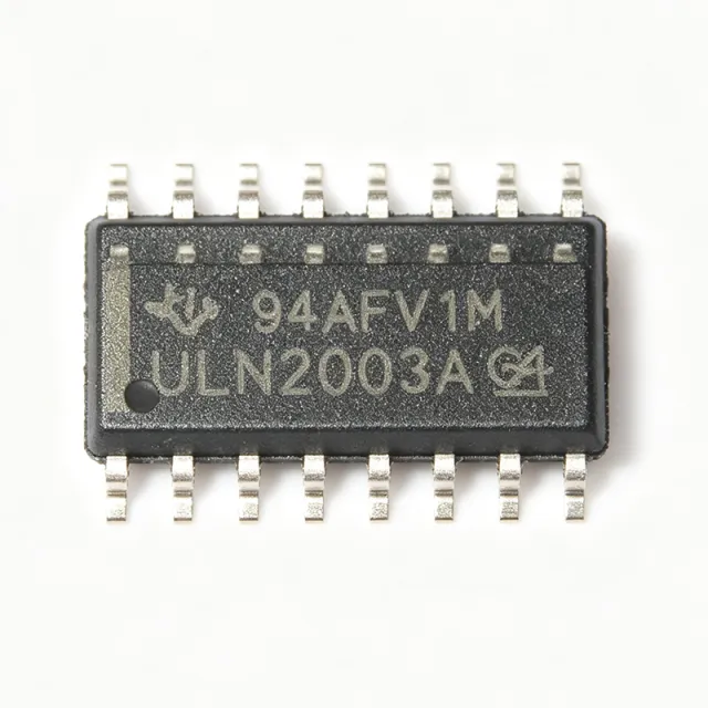
The Texas Instruments ULN2003AD is a 7-channel high-voltage, high-current Darlington transistor array designed for driving inductive loads such as relays, solenoids, stepper motors, and lamps. It features seven open-collector Darlington pairs with common-cathode clamp diodes for inductive transient suppression, and is available in a 16-pin SOIC (D) package. Each channel can sink up to 500 mA continuously and 600 mA peak, with a collector-emitter voltage rating of 50 V. The device operates over a temperature range of -40°C to +105°C and is RoHS compliant. A Darlington transistor array is a semiconductor device that integrates multiple Darlington pairs, each consisting of two bipolar transistors in a configuration that provides high current gain. This category falls under the hierarchy: Darlington array -> transistor array -> discrete semiconductor -> semiconductor. The ULN2003A is a specific variant of the ULN2003 family, which is widely used in industrial and consumer applications for interfacing low-level logic signals to high-current loads. Key features include seven Darlington pairs with a total current capability of 500 mA per channel, a collector-emitter voltage rating of 50 V, and integrated clamp diodes for inductive load protection. The input is compatible with TTL and 5V CMOS logic, and the device includes a common emitter for all channels. The SOIC-16 package provides a compact footprint for space-constrained designs. The ULN2003AD uses a bipolar process technology with a high-current NPN Darlington configuration. Each channel has a base resistor (2.7 kΩ) and an emitter resistor (3.6 kΩ) to ensure proper biasing and thermal stability. The integrated clamp diodes are connected to a common cathode pin (pin 9) for easy connection to the supply rail. The device exhibits a low saturation voltage (typically 1.6 V at 350 mA) to minimize power dissipation. Typical applications include relay drivers, stepper motor drivers, solenoid drivers, and lamp drivers in industrial control, automotive, and consumer electronics. The high current gain allows direct interfacing with microcontrollers without additional driver stages, simplifying circuit design. When designing with this device, ensure that the total power dissipation does not exceed the package thermal limits. For high-current applications, consider using multiple channels in parallel or adding external heatsinking. The clamp diodes must be connected to the positive supply rail to protect against inductive kickback. This page synthesizes distributor pricing, drop-in alternatives, and practical design notes not found in the TI datasheet, providing a comprehensive resource for engineers selecting the ULN2003AD.

ULN2003ADR - 50V 500mA 7-ch Darlington Array SOIC-16 | TI
The Texas Instruments ULN2003ADR is a high-voltage, high-current Darlington transistor array containing seven NPN Darlington pairs in a 16-pin SOIC (D) surface-mount package. Each channel is rated for 500 mA collector current and 50 V collector-emitter voltage, with integrated common-cathode clamp diodes for inductive load driving. The device includes 2.7 kOhm series base resistors on every input, allowing direct interface with TTL or CMOS logic at 3.3 V or 5 V without external components. A Darlington transistor array is a monolithic IC that integrates multiple high-gain Darlington-pair switches, each formed by two cascaded bipolar transistors whose collectors tie together and whose emitters drive the load. Within the broader taxonomy, the ULN2003ADR sits under: transistor array -> bipolar transistor array -> Darlington array -> driver IC -> semiconductor. Each pair typically delivers beta > 1000, so a few milliamps of input current can switch hundreds of milliamps at the output. This integration simplifies board design by replacing seven discrete NPN transistors plus seven base resistors with a single 16-pin IC. Key features include 500 mA continuous collector current per channel, 50 V minimum output breakdown, integrated flyback diodes, and logic-level inputs compatible with 3.3 V and 5 V microcontrollers. The open-collector outputs allow flexible pull-up voltage selection independent of the logic supply. The SOIC-16 (D) package offers a small footprint suitable for reflow soldering, with all seven channels and the common-cathode clamp brought out for easy PCB routing. The architecture is bipolar; the seven Darlington pairs share a common emitter (substrate) tied to the GND pins. Total power dissipation for the package is approximately 0.95 W at 25 C, derating linearly with temperature. Channel-to-channel matching is tight because all pairs share the same silicon die, which is critical for stepper motors and multi-coil relay banks requiring matched drive strength. Typical applications include unipolar stepper motor drivers, relay and solenoid drivers, lamp and LED matrix drivers, and logic-level buffers for higher-current loads. In each case the ULN2003ADR replaces discrete driver circuits with a single IC, reducing PCB area and BOM count. When designing with this device, ensure that the total package dissipation stays below the derated limit by calculating the worst-case voltage drop across each conducting Darlington and summing across active channels. The clamp diodes handle inductive kickback, but the user must still size the supply decoupling appropriately for the load.

ULN2003AN - 50V 500mA 7-Ch Darlington Array | TI | DIP-16
The Texas Instruments ULN2003AN is a high-voltage, high-current Darlington transistor array consisting of seven open-collector NPN Darlington pairs rated at 50V and 500 mA per channel, housed in a 16-pin PDIP (N) through-hole package. Each pair integrates two bipolar transistors in a Darlington configuration, yielding typical current gain of approximately 1000 (beta min 1000 per the manufacturer datasheet) at low input currents, allowing direct drive from CMOS, TTL, and 5V microcontrollers. Integral common-cathode clamp diodes tied to a dedicated COM pin permit direct switching of inductive loads such as relay coils, unipolar stepper motors, and solenoids without external freewheeling circuitry. A Darlington transistor array is a class of bipolar (BJT) integrated circuit that bundles multiple high-gain Darlington pairs on a single die, acting as a low-side driver. Within the broader taxonomy, it belongs to the discrete transistor category, sits below generic BJT arrays, and is widely classified as an interface/driver IC for relay, lamp, and motor loads. The ULN2003 family is the de-facto industry standard for 7-channel low-side switching from logic-level inputs, making it one of the longest-lived and most cloned ICs in the market. Key features include seven identical Darlington output stages, 50V minimum collector-emitter sustaining voltage, 500 mA continuous collector current per channel (peak to 600 mA), built-in output clamp diodes for inductive load protection, inputs compatible with TTL/CMOS/PMOS/DTL logic, and an operating junction temperature range up to 150 C. The input pins present a series base resistor suitable for 3.3V and 5V logic; no external resistor network is required. Architecturally, each channel pairs a driver transistor (Q1) and an output transistor (Q2) to multiply beta, with integrated 2.7 kohm base resistors on every input. This monolithic bipolar process yields predictable saturation behavior (Vce(sat) ~0.9-1.0V at low currents, ~1.1V at 350 mA) but introduces a measurable Vce drop that dissipates substantial power in high-current applications. Typical applications include 5V relay driver cards, unipolar stepper motor driver boards (commonly paired with 28BYJ-48 motors), LED matrix row/column drivers, solenoid valves, DC brushed motor direction switches, and lamp/display drivers. Hobby and educational platforms (Arduino shields, Raspberry Pi HATs) frequently adopt the ULN2003AN because of its robust 500 mA rating and zero-firmware footprint. Designers should budget headroom for the ~1V collector-emitter saturation drop and derate output current as duty cycle rises. The thermal resistance of PDIP-16 (theta_JA ~70 C/W typical) limits total package dissipation to roughly 1.5W without airflow, so high-current loads should be distributed across multiple channels rather than concentrated on a single pair. This page synthesizes distributor pricing for the original TI part plus cloned second-source options, a drop-in alternative table for sourcing resilience, and practical PCB/application guidance beyond what the manufacturer datasheet covers in isolation.
ULN2003ANE4 - 7-Ch NPN Darlington 500mA 16-PDIP | TI
The Texas Instruments ULN2003ANE4 is a high-voltage, high-current Darlington transistor array containing seven NPN Darlington pairs in a 16-pin PDIP through-hole package. Each channel is rated for 50V collector-emitter breakdown and 500mA continuous collector current, with built-in common-cathode clamp diodes for inductive load switching. The input pins are designed for direct CMOS, TTL, and 3.3V MCU logic interfacing through integrated base resistors. A Darlington transistor array is a monolithic IC that integrates multiple Darlington-pair drivers in a single package, allowing microcontrollers and low-power logic to switch high-current loads such as relays, solenoids, lamps, and stepper motor windings. Each Darlington pair multiplies the input current by the product of the two transistor betas, producing very high current gain (typically 10,000+) and enabling a logic-level signal to drive loads drawing hundreds of milliamps. The ULN2003 family sits at the low-side (open-collector) side of an H-bridge or relay driver topology, and is widely recognized as the de-facto standard driver for Arduino relay boards, 28BYJ-48 stepper motors, and unipolar stepper motor control. Key features include 7 matched channels with 500mA per-channel continuous rating, integrated 2.7kOhm base resistors for direct 5V/3.3V logic interface, built-in freewheeling diodes for inductive loads, 50V minimum VCEO breakdown, and a logic-0 input current of approximately 0.93mA at 3.85V. The 16-pin PDIP package is well-suited for breadboarding and through-hole prototyping, and the array can be paralleled (channels in parallel) for higher current applications. Typical applications include relay drivers, stepper motor drivers (especially unipolar and 28BYJ-48 gear motors), solenoid and valve drivers, LED matrix row/column drivers, logic-level shifters for power devices, and lamp/display drivers. The wide 50V breakdown supports driving 24V industrial relays and 12V automotive lamps directly from 3.3V microcontroller GPIO pins. When designing with this part, ensure PCB trace widths and copper pours can handle 500mA continuous per channel; derate to 350mA if all seven channels conduct simultaneously. The integrated clamp diodes share a common cathode tied to a dedicated pin (pin 9, COM) which must either be tied to V+ for freewheeling or left open if the load has its own flyback path.
ULN2803ADWR - 8-Channel 50V 500mA Darlington Array | TI
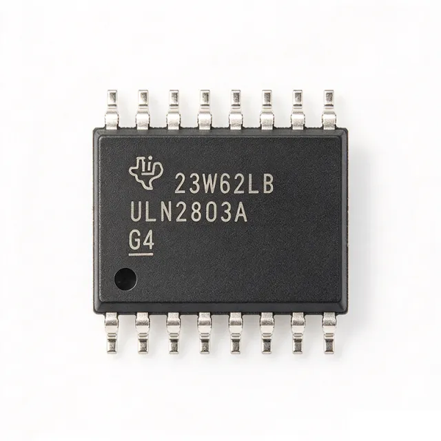
The Texas Instruments ULN2803ADWR is a high-voltage, high-current Darlington transistor array integrating eight NPN Darlington pairs into a single 18-pin SOIC (DW) surface-mount package, each rated 50 V collector-emitter and 500 mA collector current. The device features integrated common-cathode clamp diodes tied to a dedicated COM pin (pin 10) for switching inductive loads such as relays and solenoids. Logic inputs are TTL/5 V CMOS compatible via on-chip 2.7 kOhm base resistors, and channels may be paralleled for higher currents. A Darlington transistor array is an integrated circuit that combines multiple Darlington pairs - two bipolar transistors cascaded for very high current gain (hFE typically >1000) - into a single die. This category belongs to the power switch / load driver family within power-management semiconductors, sitting under the broader umbrella of discrete-array ICs. By integrating eight drivers, the part allows low-current logic outputs from microcontrollers, TTL, or CMOS gates to switch high-current loads with a minimum of external components. Key features include 50 V continuous collector-emitter rating, 500 mA continuous collector current per channel (with peak inrush capability higher due to Darlington dynamics), 2.7 kOhm input base resistors allowing direct interface to 3.3 V and 5 V logic, and built-in flyback clamp diodes tied to COM. The -40 C to +85 C operating temperature range covers industrial environments. The 18-SOIC (DW) footprint is JEDEC-standard and footprint-compatible with several legacy through-hole-to-SMD migration designs. Internally, each Darlington pair includes base and emitter resistors that set predictable turn-on thresholds and stabilize off-state leakage, while the integrated clamp diodes provide a defined current path for inductive kickback. Total package dissipation is bounded by thermal resistance; at 25 C ambient with adequate PCB copper, approximately 1.4 W is achievable. Output saturation voltage of about 1 V at rated current is the typical Darlington trade-off for high gain. Typical applications include 5 V relay driver arrays, stepper motor winding drivers (commonly with bipolar stepper motors in 3D printers, CNC machines, and robotics), solenoid and valve drivers, LED and lamp matrix drivers, and logic-level buffers. The part directly interfaces MCU GPIO to high-current loads in a single SOIC-18 footprint, eliminating discrete transistor driver stages. Always connect the COM pin (pin 10) to the positive supply of the inductive load so the clamp diodes can absorb back-EMF. Budget total package dissipation across all active channels and use adequate copper pour. This device is in Last Time Buy - consider drop-in alternatives below for new designs. This page synthesizes distributor stock, drop-in alternatives, and practical design notes not consolidated in the manufacturer datasheet, helping engineers migrate from this LTB part with minimal PCB rework.

ULN2803APG - 8ch Darlington Sink Driver, 50V, 500mA DIP-18
The Toshiba ULN2803APG is an 8-channel high-voltage, high-current Darlington sink driver housed in a 18-pin DIP (through-hole) package. It integrates eight NPN Darlington pairs with integral clamp diodes for switching inductive loads, delivering up to 500 mA per channel and 50 V collector-emitter breakdown voltage. Each Darlington pair features a base-emitter input resistor of 2.7 kOhm, allowing direct CMOS/TTL logic interface at 5 V inputs. A Darlington transistor array is a monolithic bipolar IC that pairs two NPN transistors so the emitter of the first drives the base of the second, multiplying current gain (hFE typically > 1000). Eight such pairs share a common-emitter ground pin, forming an 8-channel low-side switch well suited to driving relays, solenoids, stepper motor windings, lamp filaments, and LED displays from low-power digital logic. The ULN2803 family sits within the broader hierarchy of bipolar transistor arrays → interface ICs → driver ICs → power management. Key specifications of the ULN2803APG include 500 mA continuous collector current per channel, 50 V VCEO sustain voltage, integrated free-wheeling clamp diodes on each output for inductive load protection, and an input structure compatible with 5 V CMOS logic levels. The DIP-18 footprint matches industry-standard pinouts used by competing parts from TI, STMicroelectronics, and Allegro, simplifying PCB migration. Typical applications span relay drivers in industrial control, hammer/lamp drivers in point-of-sale and copier equipment, LED/display matrix drivers, and stepper or DC motor bridge half-drivers. The integrated clamp diodes eliminate external snubbers on solenoids and relay coils, reducing BOM count and improving long-term reliability against back-EMF transients. When designing with this device, observe the package power dissipation limit of 760 mW for the DIP-18 variant and derate per channel when multiple outputs switch simultaneously at high duty cycle. The common-emitter architecture makes the ULN2803APG strictly a low-side (sink) driver — for high-side (source) driving use the complementary ULN2803 family high-side counterpart or a PNP/PMOS array.
ULN2803APG5M - 8ch 50V/500mA Darlington Sink Driver | Toshiba
The Toshiba ULN2803APG5M is a monolithic high-voltage, high-current Darlington transistor array comprising eight NPN Darlington pairs with integral clamp diodes for inductive-load switching. Each Darlington channel is rated to 50 V collector-emitter and 500 mA continuous collector current (760 mW total package dissipation), making it a true 8-channel open-collector sink driver in a 18-DIP through-hole package. The (5,M) suffix indicates 5-piece minimum order pack shipped from the Toshiba tube / tray manufacturing flow. A Darlington transistor array is a class of bipolar driver in which two transistors are cascaded (collector of the input transistor tied to the base of the output transistor) so that the input sees only the very small base current of the first device, while the output stage delivers the load current. The resulting current gain (hFE) of several thousand allows logic-level signals (5 V CMOS, 3.3 V TTL, or even microcontroller GPIO) to directly switch much higher currents and voltages. Within the broader taxonomy, the ULN2803APG5M belongs to the Bipolar Transistor Array (BJT array) family, sits inside the Power Management / Interface & Driver category, and ultimately functions as a low-side (sink) driver. The integral freewheeling clamp diodes across each output protect the IC when driving relays, solenoids, and motors from the inductive kick that would otherwise destroy the output transistors. Key differentiating features include eight parallel channels in one package (saving PCB area versus discrete transistors), 50 V rating that comfortably covers 24 V industrial and automotive relays, 500 mA continuous per channel (higher peaks possible within SOA limits), built-in input resistors for direct 5 V logic compatibility, and the 18-DIP through-hole footprint that remains the industry standard for breadboarding, legacy designs, and pin-compatible cross-brand substitutions. Compared with discrete MOSFETs, the Darlington array offers simpler drive and lower BOM cost but trades away switching speed, so it is best suited for slow on/off actuation rather than high-frequency PWM. The architecture uses eight common-emitter Darlington switches whose emitters are tied to a common ground pin, while each open collector is brought out separately to a DIP pin. The clamp diode anode connects to Vsup and cathode to each collector, suppressing flyback voltage transients. Total power dissipation of 760 mW for the package (about 95 mW per channel continuous) defines the safe envelope. Typical applications include 5 V logic-to-24 V relay driver boards, stepper motor phase drivers for small unipolar motors, solenoid and valve drivers, LED matrix row/column drivers, thermal printer head drivers, and lamp/indicator banks. When designing with this device, always verify package dissipation against the worst-case simultaneous-channel conduction: eight 100 mA outputs will exceed the 760 mW package rating unless derated.
ULN2803APGCNHZN - 8ch Darlington Sink Driver 50V/500mA DIP-18 | Toshiba
The Toshiba ULN2803APGCNHZN is an 8-channel high-voltage, high-current Darlington sink driver array housed in a 18-pin DIP package. Each of the eight NPN Darlington pairs can sink up to 500 mA continuously and is rated for 50 V collector-emitter voltage, with integral free-wheeling clamp diodes for switching inductive loads such as relays, solenoids, stepper motors and small DC loads. A Darlington transistor array is a type of bipolar junction transistor (BJT) driver that pairs two transistors in a Darlington configuration to multiply current gain (hFE), allowing a low-current logic signal (such as a 5 V TTL or 3.3 V CMOS microcontroller output) to switch high-current loads. Within the broader semiconductor taxonomy, the ULN2803 belongs to the power transistor array family, which sits under interface ICs and power management ICs used to bridge low-power digital controllers and high-power actuators. Eight such drivers are integrated into a single package, providing a compact, pin-efficient solution for multi-channel switching. Key features include 500 mA continuous collector current per channel, 50 V minimum collector-emitter breakdown voltage, integral clamp diodes for inductive load protection, TTL/CMOS-compatible inputs via the 2.7 kOhm base resistor network, and an 18-pin DIP (through-hole) package that simplifies prototyping and breadboard use. The 8-channel parallel architecture allows simultaneous control of multiple loads using a single IC, reducing BOM and PCB area. The device is fabricated using a bipolar junction transistor (BJT) process optimized for high-voltage, high-current switching. The monolithic silicon construction provides matched base resistors per channel, ensuring consistent drive behavior across all eight outputs, while the common-cathode clamp diodes tied to a dedicated COM pin simplify inductive load management. Typical applications include relay drivers, solenoid drivers, stepper motor unipolar winding drivers, LED matrix row/column drivers, lamp drivers, logic-level translators, and general-purpose high-current sink switching for industrial automation, consumer appliances, and HVAC controls. In microcontroller-based designs, the ULN2803 typically sits between a 5 V GPIO and a 24 V load bus. When designing with this part, ensure that the sum of all simultaneously-active channel currents does not exceed the package's total power dissipation of approximately 1.47 W, and always connect the COM pin to the positive supply when driving inductive loads so that the internal clamp diodes can recirculate the back-EMF. Avoid exceeding the 50 V VCEO rating, especially with inductive kick. This page synthesizes distributor pricing, drop-in same-package and cross-brand alternatives, and practical design notes not found in a single manufacturer datasheet, helping engineers shortlist a working part quickly.
ULN2803APGOM - 8CH 50V 500mA Darlington Sink Driver DIP-18 | Toshiba
The Toshiba ULN2803APGOM is an 8-channel high-voltage, high-current Darlington sink driver in an 18-pin PDIP (DIP-18) through-hole package. Each of the eight channels integrates an NPN Darlington pair rated at 50 V collector-emitter voltage and 500 mA continuous collector current, with integral free-wheeling clamp diodes for switching inductive loads such as relays, solenoids, and stepper motor windings. The CMOS-compatible 5 V logic inputs simplify direct connection to modern microcontrollers, and the (O,M) Toshiba marking suffix indicates factory-packaging/tray code rather than an electrical variant. A Darlington sink driver is a type of integrated bipolar transistor array that provides high current gain by cascading two NPN transistors inside a single package. The ULN2803APGOM belongs to the bipolar transistor array -> Darlington transistor array -> power management IC hierarchy. By sinking current to ground (low-side switching), it allows a low-power logic output to control high-power loads that would otherwise damage a microcontroller I/O pin. This topology is widely used for interface between digital control circuits and electromechanical actuators. Key specifications include a minimum DC current gain (hFE) of approximately 2000 at low collector current due to the Darlington cascade, an input series base resistor of 2.7 kOhm sized for 5 V CMOS logic, and an integral collector-emitter clamp diode on every channel rated for switching inductive transients. The package dissipates up to 2.25 W at 25 C ambient, derating linearly to zero at 125 C. The 18-pin PDIP form factor supports easy breadboarding and through-hole PCB prototyping. Typical applications include relay and solenoid drivers for industrial automation, unipolar stepper motor winding drivers, LED matrix row/column sinks, inkjet printer head drivers, and lamp/display drivers. The eight parallel channels also make it useful for multi-axis low-side switching in robotics and HVAC controls. When designing with this part, ensure that the total package dissipation does not exceed 2.25 W at 25 C ambient with appropriate linear derating above 25 C. Place flyback clamp diodes (already integrated) will protect the device when switching inductive loads, but external free-wheeling diodes or snubbers may be needed for very fast switching edges.

UM4306B - Si PPIN Hermetic Glass Axial RF Diode | Microchip
The Microchip UM4306B is a silicon PIN diode in a hermetic glass axial package, engineered for high-frequency switching and attenuator applications up to the UHF band. The device combines an intrinsic-region (I-region) silicon die with low thermal resistance construction, yielding low-distortion performance suitable for very low distortion linear attenuators, RF switches, and specialized functions. A PIN diode is a specialized diode structure in which a high-resistivity intrinsic semiconductor region (the "I-layer") is sandwiched between the P and N regions. Under forward bias, charge carriers flood the I-layer, lowering its RF resistance; under reverse or zero bias, the diode presents a near-open circuit. This behavior makes PIN diodes ideal for controlling RF signals in switch, attenuator, limiter, and phase-shifter circuits across a wide frequency range, behaving as a current-controlled variable resistor at RF. Key features of the UM4306B include very low intermodulation distortion, a thick intrinsic region for high RF voltage handling, hermetic glass axial packaging for environmental robustness, and a low thermal resistance construction that supports high average power dissipation. These attributes allow the UM4306B to be deployed where harmonic and intermodulation performance are critical, particularly in multi-carrier or broadband RF signal chains. Technically, the part belongs to the UM4300/UM7300 PIN diode family. The thick I-layer gives the diode a high breakdown voltage and high carrier lifetime, enabling it to handle significant RF power while maintaining a low distortion floor. The hermetic glass axial (axial-lead) package protects the silicon die from moisture and contamination, supporting long-term reliability in outdoor, military, and aerospace-grade RF front ends. Typical applications include RF switching matrices, PIN diode attenuators, AGC loops, TR switches in radar and radio transceivers, RF test equipment, and broadband signal-routing networks. Designers favor the UM4306B in designs that demand both low distortion and high reliability. When designing with this device, observe the recommended bias currents from the manufacturer datasheet and verify that the package's thermal path (lead soldering) can dissipate the intended RF power. Designers should match the bias network to the carrier-frequency band of operation. This page synthesizes distributor pricing, drop-in alternatives, and practical design notes not found in the manufacturer datasheet, providing an information gain over distributor-only listings for engineers evaluating the UM4306B.
UM7006B - 600V 5.5W RF PIN Diode | Microchip Technology
The Microchip UM7006B is a single-junction RF PIN diode rated for 600 V reverse voltage and 5.5 W continuous power dissipation, packaged in an axial-lead hermetic body. It is part of the UM7000 series of high-power PIN diodes originally developed by Microsemi and now carried by Microchip Technology after the 2018 Microsemi acquisition. The diode targets RF switching, attenuation, and limiter applications where moderately high power handling must coexist with low series resistance and low capacitance. A PIN diode is a semiconductor device with an intrinsic (undoped) semiconductor region sandwiched between p-type and n-type regions. Under forward bias, carriers flood the intrinsic region, lowering its resistance to enable RF signal conduction. Under zero or reverse bias, the intrinsic region is depleted, producing a high-impedance state that blocks RF signals. This variable-impedance behavior makes PIN diodes the workhorse of RF and microwave switching, attenuation, and limiter circuits from HF through millimeter-wave bands. Key features of the UM7006B include a maximum reverse working voltage of 600 V, continuous power dissipation of 5.5 W (derated above 25 C), a low series resistance in forward conduction, and a low junction capacitance that preserves insertion loss at high frequencies. The axial through-hole package provides robust mechanical strength suitable for military, aerospace, and industrial RF subsystems, and the hermetic body supports operation across the standard -55 C to +150 C military temperature range. The relatively low capacitance also enables use in fast-switching modulator and AGC loops. Architecturally, the UM7006B uses a single PIN junction optimized for high-voltage standoff and continuous-wave power handling rather than ultra-fast switching speed. Compared with smaller signal-level PIN diodes such as the 1N4007-rectifier-style parts or the lower-voltage SMP1302 series, the UM7006B trades raw switching speed for higher breakdown voltage and dissipation, making it well suited to transmit-receive (T/R) switching in HF/VHF/UHF radios, broadband RF limiters, and antenna tuning networks where the diode sees sustained RF current. Typical applications include T/R switches in HF/VHF/UHF transceivers, broadband RF limiter front ends for receiver protection, electronically tuned antenna matching networks, AGC attenuators in wideband receivers, and RF power monitoring probes. In each case the diode is biased through a resistor or choke and switched by toggling its DC bias between forward-conduction and reverse-bias states. When designing with the UM7006B, account for the 5.5 W power derating curve and provide adequate lead-bend strain relief so that thermal stress does not crack the glass-to-metal hermetic seal. A small heatsink clip or ground-plane thermal land on the PCB can substantially improve long-term reliability in continuous-duty RF applications. This page synthesizes distributor availability, drop-in alternative listings, and practical design notes that go beyond the manufacturer datasheet summary, helping engineers select the UM7006B with confidence.
UM9301 - 75V PIN Attenuator/Switch Diode | Microchip Technology
The Microchip Technology UM9301 is a silicon PIN diode housed in an axial glass-leaded (DO-35-like) hermetic package. It is rated for 75 V maximum reverse voltage, 1 W power dissipation, and is designed for both RF switch and attenuator applications in HF through microwave frequencies. A PIN diode is a semiconductor device with an intrinsic (undoped) high-resistivity "I" region sandwiched between P-type and N-type regions. Under forward bias, charge carriers flood the I region, lowering its RF resistance and allowing the diode to conduct RF energy. Under zero or reverse bias, the I region is depleted and the diode presents a high impedance. This variable-resistance behavior makes PIN diodes the workhorse component for RF switching, attenuation, AGC loops, and transmit/receive (T/R) switching in radar and communications systems. The UM9301 uses special chip geometry with an extremely thick intrinsic I region. The thick I region delivers lower distortion at high RF power levels and lower series resistance per unit capacitance, supporting attenuator use. Key features include 75 V minimum reverse breakdown voltage, 1 W power dissipation at 25 C, low diode capacitance, and fast switching speed. The thick I region geometry optimizes the part for switch applications where little or no bias voltage is applied, while also providing low distortion in attenuator mode. Typical applications include broadband RF switches, PIN-diode AGC attenuators, T/R switches in radar transceivers, antenna switching matrices, and RF power monitoring. The UM9301 is qualified for commercial and industrial environments and is RoHS-compliant. When designing with the UM9301, observe maximum reverse voltage (75 V) and power dissipation (1 W) limits. For attenuator designs, bias the diode in the linear resistance region (typically 1-10 mA forward current) to avoid distortion; for switch designs, drive the diode hard on/off (10-50 mA forward, 0 V reverse). Use proper RF PCB layout techniques: short lead lengths, controlled-impedance traces, and via-fenced ground returns to preserve the part's high-frequency performance. This page synthesizes distributor pricing, drop-in same-package alternatives, and practical RF design notes not found in the manufacturer datasheet.

UM9369 - Semiconductor Device, NSN 5961-01-697-9746 | Microchip (Microsemi)
The Microsemi (a Microchip Technology company) UM9369 is a semiconductor device registered under US National Stock Number 5961-01-697-9746 (FSC 5961, Semiconductor Devices and Associated Hardware), supplied by the Microsemi Frequency and Time product group under part category 1B0C5. According to the NSN records retrieved from distributor and NSN lookup databases, this FSC class describes a two-electrode semiconductor device with an asymmetrical voltage-current characteristic - the defining property of a diode-class component. A diode is the most fundamental semiconductor device: it permits current flow primarily in one direction, from anode to cathode, and blocks reverse current up to a rated reverse voltage. Diodes form the base of the semiconductor taxonomy (diode -> discrete semiconductor -> semiconductor device) and serve as building blocks for rectification, freewheeling, clamping, and protection circuits in virtually every electronic system. Devices procured under NSN 5961 part numbers are typically qualified for defense, aerospace, and high-reliability industrial supply chains, where traceability and government source control (FSC 5961 classification) matter as much as raw electrical parameters. Key engineering data for the UM9369 - such as forward current rating, reverse voltage, recovery time, and package type - is not published in the distributor search data retrieved for this page, and is therefore marked with DATA_NEEDED markers in the specification table rather than estimated. Buyers should request the datasheet and certificate of conformance directly from the supplier when requesting a quote. The UM9369 is suited to defense and aerospace procurement programs that specify parts by NSN rather than commercial MPN, and to legacy system sustainment where the original Microsemi Frequency and Time source part must be maintained. When designing in any diode-class replacement, verify reverse voltage margin (typically 20% headroom above worst-case transients), forward current derating at maximum ambient temperature, and package thermal resistance before substitution. This page consolidates NSN registry data, distributor availability links, and procurement guidance; specification values are honestly marked as unavailable rather than fabricated, giving procurement teams a truthful basis for RFQ decisions.