SN74LVC1G3157DCKR
SN74LVC1G3157DCKR - SPDT Analog Switch, 15Ohm, SC-70-6 | TI
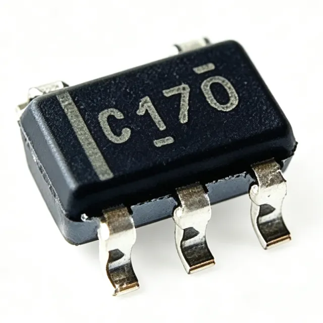
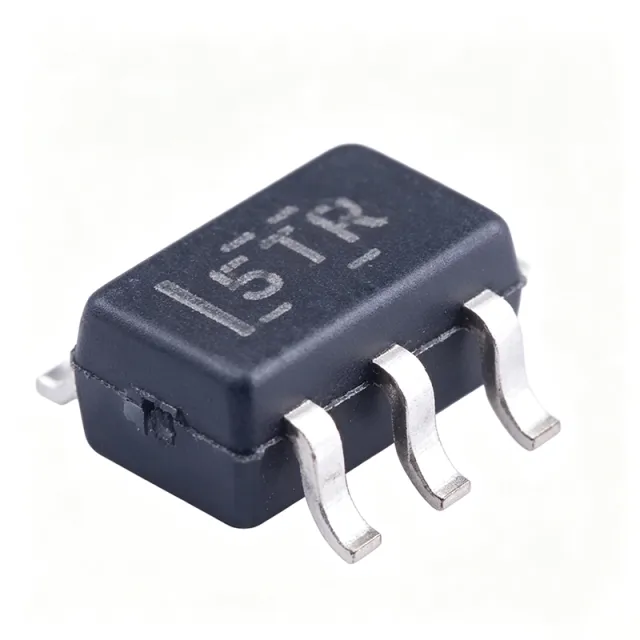
The Texas Instruments SN74LVC1G3157DCKR is a single-channel single-pole double-throw (SPDT) analog switch designed for 1.65V to 5.5V VCC operation, housed in a 6-pin SC-70 (DCK) package. Key parameters include a typical on-state resistance of 15 ohm, a wide 340 MHz bandwidth, and a propagation delay of typically 0.5 ns at 50 pF load, making it suitable for both analog and digital signal routing.
An analog switch (also called a bilateral switch or pass gate) is a semiconductor device that uses CMOS transmission gates to connect or isolate two signal paths under logic-level control. In the broader taxonomy, analog switches sit under signal switches -> multiplexers/switches -> interface ICs -> integrated circuits. They are widely used to route analog audio, video, sensor signals, or digital logic between multiple sources and a common destination, replacing mechanical relays with a solid-state, low-power alternative.
Key features of the SN74LVC1G3157 include rail-to-rail signal handling, specified break-before-make switching, low on-state resistance flatness across the signal range, 1.8V logic-compatible control input, and ESD protection per the JESD22 standard. The device supports 5V tolerant signal passing even when VCC is only 1.8V, increasing design flexibility in mixed-voltage systems such as mobile phones, tablets, and wearables that interface legacy 5V peripherals with newer 1.8V cores.
Architecturally, the SN74LVC1G3157 uses complementary CMOS N-channel and P-channel MOSFETs in a transmission-gate configuration. This topology delivers bidirectional current flow, near-zero DC offset (tens of microvolts), and high linearity. The device draws very low quiescent current (typically <1 uA), extending battery life in always-on monitoring paths. ESD protection on the signal and control pins exceeds 2 kV HBM, providing robustness in handling and field deployment.
Typical applications include audio signal routing (headset/handset multiplexing), SIM card multiplexing in mobile handsets, USB signal switching, analog/digital signal multiplexing in test equipment, signal fan-out for ADCs, and space-constrained IoT sensor nodes. The SC-70-6 footprint occupies only 2.0 mm x 1.25 mm of board area, ideal for compact consumer designs.
When designing with this device, place ceramic bypass capacitors (0.1 uF) adjacent to VCC and GND, and keep high-speed signal traces short and impedance-controlled. Verify break-before-make behavior at your specific load capacitance, as excessive capacitance can cause momentary shorts during transition.
This page synthesizes distributor pricing, drop-in SC-70-6 alternatives, and practical signal-integrity design notes not consolidated in any single manufacturer datasheet.
USD $0.22
有现货