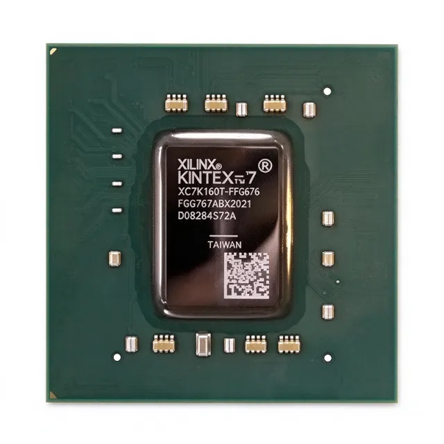
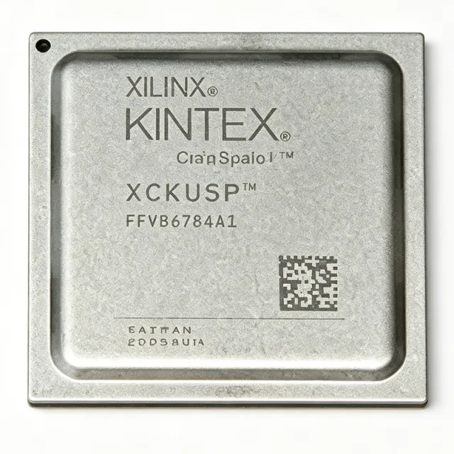
XCKU035-1FBVA676C
XCKU035-1FBVA676C Kintex UltraScale FPGA 444K Cells | AMD
The AMD Xilinx XCKU035-1FBVA676C is a Kintex UltraScale Field Programmable Gate Array built on TSMC's 20nm process, integrating 444,343 logic cells and 19,456,000 system gates in a 676-ball FCBGA package (27 mm × 27 mm) with 312 user I/Os. It runs a -1 speed grade targeting up to 630 MHz fabric performance, with 12.5 Gb/s capable transceivers (GTH) on select Kintex UltraScale SKUs and 240 DSP48E2 slices optimized for high-throughput fixed- and floating-point arithmetic. The commercial temperature grade (suffix C) supports 0 °C to +85 °C operation with a 0.95 V core voltage.
What is an FPGA? A Field Programmable Gate Array (FPGA) is a programmable logic device that lets designers implement custom digital circuits after PCB fabrication by configuring an array of configurable logic blocks (CLBs), dedicated DSP slices, block RAM, and high-speed serial transceivers. Within the broader semiconductor hierarchy, an FPGA sits between general-purpose CPUs/GPUs (fixed instruction set, software-defined) and ASICs (fixed hardware). AMD's Kintex UltraScale family occupies the mid-range position in the UltraScale portfolio, sitting below Virtex UltraScale (highest logic density and bandwidth) and above Artix UltraScale (lowest cost and power). All Xilinx boards shift the value curve toward best-in-class price/performance/watt at 20nm.
Key features of the XCKU035-1FBVA676C include up to 1,250 Mbps of DDR4 external memory interface support, integrated PCIe Gen3 hard cores, 4.7 Mb of distributed RAM, 240 DSP slices, and 16 GT transceivers on -1 speed grade parts in the larger Kintex UltraScale family. The device provides 312 high-performance SelectIO pins supporting multiple I/O standards including LVDS, HSTL, SSTL, and differential memory interfaces. The device also exposes 3 MMCM and 8 PLL mixed-mode clock managers for high-frequency clock synthesis and skew management.
Architecturally, the Kintex UltraScale device uses UltraScale architecture enhancements over 7-series FPGAs - including new routing interconnect, more efficient clock networks, and improved block RAM and DSP resources. The 20nm planar CMOS process allows higher integration while keeping leakage power low, and the GT(GTH) transceivers support 12.5 Gb/s line rates for backplane and chip-to-chip serial interconnect.
The XCKU035-1FBVA676C serves wireless baseband processing, software defined radio, high-definition video processing pipelines, high-speed serial backplane bridging, and PCIe accelerator card designs in the 100K–500K logic-cell density class. When laying out a board with this BGA, allocate 12 power rails (VCCINT, VCCAUX, VCCO, MGTAVCC, MGTAVTT, VBATT, MGTVCCAUX, VCCADC, VCCBRAM, VCCO_HP, VCCAUX_IO, plus GT helper rails) and follow the package-specific K7-PCB decaps guidance in UG583 to control simultaneous switching noise and SSN.
USD $467.66
有现货