XC7A15T-2FTG256C
XC7A15T-2FTG256C - 16,640 LEs Artix-7 FPGA | AMD
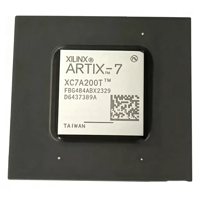
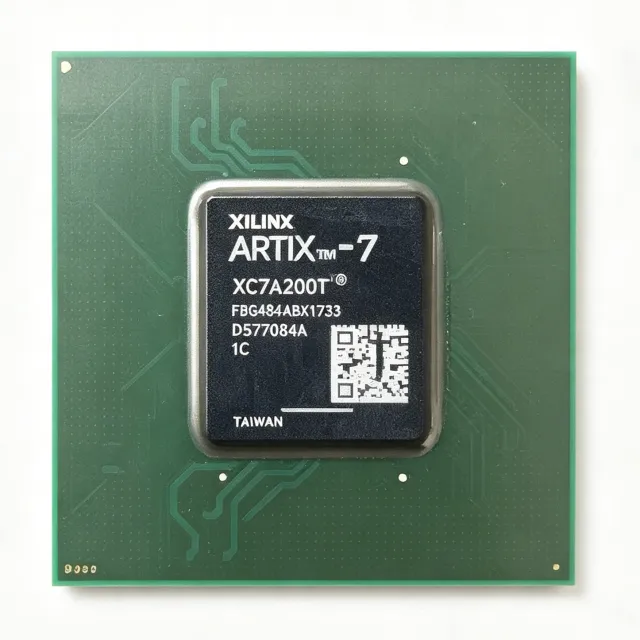
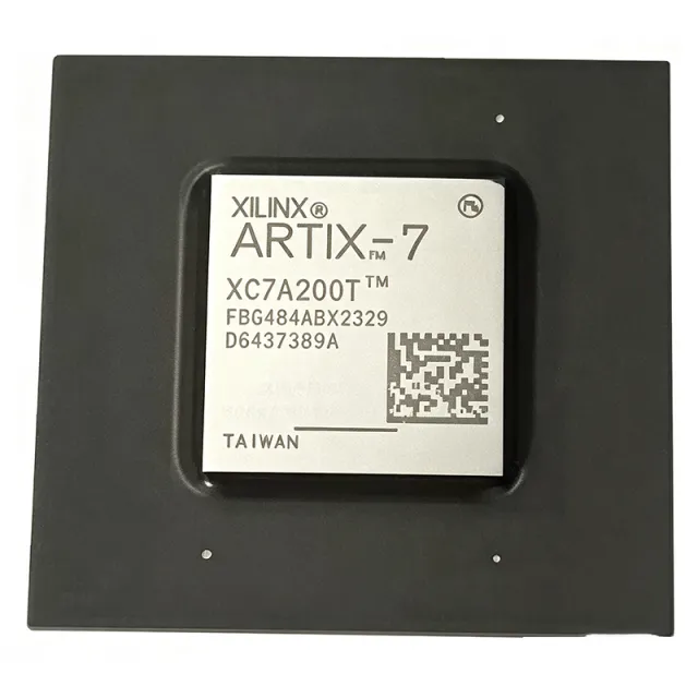
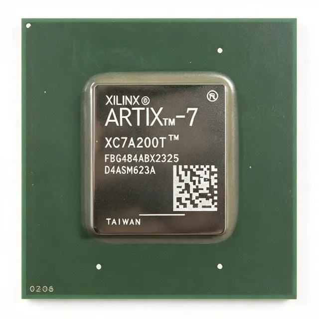
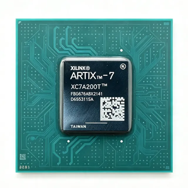
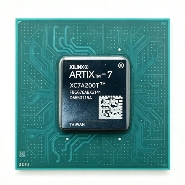
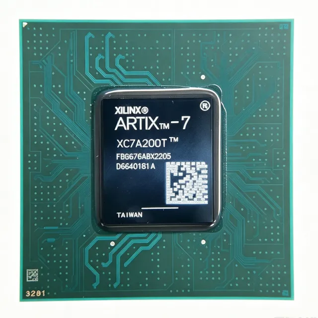
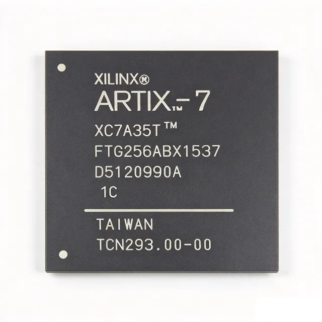
AMD XC7A15T-2FTG256C is an Artix-7 field-programmable gate array with 16,640 logic cells, 170 I/O, 921,600 RAM bits, and a 256-LBGA package. The -2 speed grade is intended for cost-sensitive, power-efficient designs requiring a balanced combination of programmable logic, DSP processing capability, and high-speed serial connectivity. It operates across the commercial temperature range of 0°C to +85°C and is available from distributors as a 256-LBGA FPGA.
An FPGA is a reconfigurable digital semiconductor in which the logic, interconnections, and processing resources are configured after manufacture. Within the product hierarchy, the XC7A15T belongs to the Artix-7 FPGA family and combines a programmable logic array, block RAM, DSP resources, and general-purpose input/output blocks in one device. This integration allows designers to implement parallel data processing, control logic, protocol bridging, and interface functions on a single programmable chip.
The principal verified device figures are 16,640 logic cells, 921,600 RAM bits, 170 I/O, and a 256-LBGA package. The -2 designation identifies its performance grade within the Artix-7 family. Its low-cost and power-efficient positioning makes it relevant to industrial automation, machine vision, telecommunications infrastructure, protocol conversion, baseband processing, wireless backhaul, and embedded control systems. The 256-LBGA package also supports compact, high-density board layouts.
Technically, the device combines programmable logic fabric with dedicated memory and DSP blocks, allowing multiple data paths to be processed concurrently. The large 170-I/O count provides substantial connectivity for external memory, sensors, network transceivers, display interfaces, and control peripherals. Its 921,600 RAM bits support buffering and data storage within the FPGA fabric, while the dedicated DSP capability enables fixed-point filtering, transform, and signal-processing functions without requiring separate accelerators.
Typical implementations place the FPGA beside high-speed transceivers, external memory, clock sources, and application-specific peripherals. Machine-vision designs can parallelize image acquisition and filtering, telecom equipment can perform line-card adaptation or protocol bridging, and industrial controllers can combine sensor acquisition with deterministic logic. Because FPGA resources are configurable, the same family can support multiple product variants without changing the PCB footprint when device density and speed-grade requirements permit.
Designers should review the manufacturer Artix-7 datasheet and package pinout files before assigning bank voltages, clock pins, high-speed serial pins, and power rails. Decoupling, PCB return paths, thermal management, configuration interface access, and proper I/O standard selection are critical to reliable implementation. Although the 256-LBGA offers high I/O density, its fine-pitch routing and power-delivery requirements demand careful constraint-driven layout and multilayer PCB planning.
This product data combines verified distributor pricing, Artix-7 family specifications, package information, and practical engineering guidance. It also distinguishes true same-package drop-in options from broader functional FPGA alternatives, helping engineers shortlist a device while still validating timing, power, configuration, and lifecycle requirements against the official AMD documentation.
询价
联系我们