产品(39,000+)

EP4CGX22CF19C7N - Cyclone IV GX FPGA 22K LE 150 I/O | Intel
EP4CGX22CF19C7N

EP4CGX22CF19C7N - Cyclone IV GX FPGA 22K LE 150 I/O | Intel

The Intel (formerly Altera) EP4CGX22CF19C7N is a Cyclone IV GX family Field Programmable Gate Array (FPGA) delivering 21,280 logic elements, 774,144 bits of embedded memory, and 150 user I/O in a 324-ball FineLine BGA (FBGA-324) package. It integrates up to two 3.125 Gbps transceivers, hardware multipliers, and PLL blocks, targeting cost-sensitive serial-protocol and digital-signal designs. The device operates from a 1.2 V core supply with additional 2.5 V/3.3 V I/O bank support, packaged in a 19 mm x 19 mm body with 1.0 mm ball pitch. A Field Programmable Gate Array (FPGA) is a programmable logic device (PLD) that combines the architecture of gate arrays with the flexibility of in-system programmability. Within the broader taxonomy, an FPGA belongs to programmable logic -> digital IC -> semiconductor. Cyclone IV GX is Intel's low-power, transceiver-equipped FPGA family positioned between the smaller Cyclone IV E and the higher-density Cyclone V series, optimized for applications requiring multi-gigabit transceivers at low static and dynamic power. Key features include 21,280 logic elements organized into 1,330 Configurable Logic Blocks (CLBs), 66 embedded 18x18 multipliers, 4 PLLs, and dual 3.125 Gbps transceivers supporting PCIe Gen1, Serial RapidIO, and Gigabit Ethernet protocols. The device supports LVDS, LVTTL, LVPECL, SSTL, and HSTL I/O standards, with per-bank programmable drive strength and slew rate. Memory resources include 774 Kbits of embedded RAM distributed across M9K blocks plus 46 Kbits of ROM. The Cyclone IV GX family uses a low-power 60 nm process technology with adaptive logic modules (ALMs) and fine-grained clock networks, achieving up to 50% lower static power than Cyclone III. The integrated transceivers feature adaptive equalization, signal detection, and CDR circuits, eliminating external PHY components for short-reach serial links. Typical applications include industrial video processing, low-cost PCIe endpoint cards, motor control, software-defined radio front-ends, and embedded vision systems. Designers typically select this device when they need integrated multi-gigabit serial I/O without the cost of larger Cyclone V or Stratix families. When designing with this device, pay attention to transceiver reference clock routing and decoupling: place 0.1 uF and 10 uF capacitors near every supply pin and follow Intel's Pin Connection Guidelines for unused transceiver channels to minimize crosstalk. This page synthesizes distributor pricing, pin-compatible same-family alternatives, and reference-design notes that go beyond the datasheet alone, helping engineers select the right OPN for production.

询价 联系我们
EP4CGX22CF19C8 - Cyclone IV GX FPGA, 21K LEs, 324-FBGA | Intel
EP4CGX22CF19C8

EP4CGX22CF19C8 - Cyclone IV GX FPGA, 21K LEs, 324-FBGA | Intel

The Intel (formerly Altera) EP4CGX22CF19C8 is a Cyclone IV GX field-programmable gate array (FPGA) with 21,280 logic elements, 774,144 bits of embedded memory, and integrated 3.125 Gbps transceivers, housed in a 324-ball FineLine BGA package at the commercial 0°C to 85°C temperature grade. Built on a low-power 60 nm process, this FPGA targets cost-sensitive applications that still require high-speed serial I/O and moderate logic density. A Cyclone IV GX FPGA is a reprogrammable logic device belonging to the programmable-logic family, sitting hierarchically below ASICs and above fixed-function ASSPs in the design flexibility spectrum. The GX sub-series adds dedicated multi-gigabit transceivers that differentiate it from the standard Cyclone IV E family, allowing direct interfacing with PCIe Gen1, Gigabit Ethernet, Serial RapidIO, CPRI, and other high-speed serial protocols without external PHY devices. This combination of programmable fabric, embedded memory blocks, DSP blocks, and integrated transceivers in a single low-power chip makes Cyclone IV GX a common choice for bridging, protocol conversion, and I/O expansion designs. Key features include 21,280 logic elements (LEs), 774 Kbits of embedded RAM (M9K blocks), 80 embedded 18x18 multipliers for DSP operations, two PLL blocks per quadrant for clock management, and a maximum of 150 general-purpose user I/O pins. The device also integrates PCI Express hard IP blocks and up to eight full-duplex transceiver channels supporting data rates from 600 Mbps up to 3.125 Gbps. Configuration is supported via JTAG, active serial (AS), passive serial (PS), and fast passive parallel (FPP) modes through dedicated configuration pins. The 324-ball FBGA package uses a 1.0 mm ball pitch, providing a compact footprint for space-constrained boards while supporting up to 150 user I/Os. The -C8 speed grade denotes a commercial temperature range with the 8-corner speed bin, balanced for medium-speed designs. Quartus II design software (or the maintained Intel Quartus Prime Lite edition) is used for synthesis, place-and-route, and bitstream generation. Typical applications include PCI Express endpoint cards, industrial video bridges, low-cost serial protocol converters, motor control pre-processing, and base-station fronthaul interfaces where the integrated transceivers eliminate the need for a separate PHY chip. Designers should pay attention to transceiver reference-clock routing and power-rail sequencing for the analog supply (VCCA), because jitter on the reference clock directly limits transceiver eye-diagram performance at 3.125 Gbps. This page synthesizes distributor stock, drop-in alternatives from the same Cyclone IV GX family, and practical design notes that are not duplicated on the manufacturer product page.

询价 联系我们
EP4CGX22CF19C8N - Cyclone IV GX FPGA 22K LE | Intel | Altera
EP4CGX22CF19C8N

EP4CGX22CF19C8N - Cyclone IV GX FPGA 22K LE | Intel | Altera

The Intel (formerly Altera) EP4CGX22CF19C8N is a low-power Cyclone IV GX FPGA with 21,280 logic elements, 774,144 bits of embedded memory, and 150 user I/Os, housed in a 324-pin LBGA (F19) package with 1.0 mm ball pitch. It integrates up to 2.5 Gbps transceivers for high-speed serial I/O and is fabricated on a low-power 60 nm process that delivers Cyclone-series cost efficiency. A Field Programmable Gate Array (FPGA) is a semiconductor device built around a matrix of configurable logic blocks (CLBs), programmable interconnect, and I/O cells that can be electrically rewired to implement arbitrary digital circuits. FPGAs occupy the middle ground between fixed-function ASICs (lower cost at volume, no flexibility) and microcontrollers (software-defined, lower throughput): they deliver hardware-level parallelism and latency for DSP, signal processing, and protocol bridging while remaining fully reprogrammable. The Cyclone IV GX family specifically adds hardened 3.125 Gbps transceiver lanes and a PCIe hard IP block, making it suited to cost-sensitive wireline and industrial bridging designs. Key specifications include 21,280 logic elements arranged into 1,330 CLB-style logic array blocks (LABs), 36 embedded 18x18 multipliers (~138 Gbps aggregate DSP throughput), and 56 Cyclone IV GX transceivers supporting data rates from 600 Mbps to 2.5 Gbps. The device supports DDR2 SDRAM interfaces up to 200 MHz and includes 4 PLLs for clock generation and synthesis. Configuration is supported through JTAG (IEEE 1149.1) and active serial/parallel flash, with built-in decompression and encryption engines. The Cyclone IV GX architecture combines a fine-grained LAB structure with embedded multiplier blocks and dedicated memory blocks (M9K) that can be configured as RAM, ROM, or FIFO. The transceiver block embeds serializer/deserializer (SERDES), word alignment, 8B/10B encoding, and pseudo-random binary sequence (PRBS) generation, eliminating the need for external PHY chips in many serial protocols. The 1.0 mm pitch LBGA package provides 150 user I/Os while remaining compatible with standard 4-layer PCB assembly. Typical applications include industrial vision and machine vision interfaces (Camera Link, CoaXPress front-ends), low-cost PCIe endpoint cards, motor control and factory automation bridges, video processing and display controllers, software-defined radio front-ends, and portable/wireless test equipment. The transceiver-rich architecture is particularly well suited to designs that previously required a dedicated PHY or an expensive mid-range FPGA. When designing with this device, pay close attention to transceiver reference clock distribution, decoupling of the analog transceiver supply pins (VCCA_PLL, VCCA_TX/RX), and signal-integrity routing of the high-speed serial lanes. The Quartus II design suite (legacy) or Quartus Prime is required for synthesis, place-and-route, and bitstream generation, and a JTAG programmer is needed for in-system configuration. This page synthesizes distributor pricing, drop-in alternatives, and practical design notes not found in the manufacturer datasheet.

询价 联系我们
EP4CGX22CF19I7 - Cyclone IV GX FPGA, 21280 LE, 324-FBGA | Intel
EP4CGX22CF19I7

EP4CGX22CF19I7 - Cyclone IV GX FPGA, 21280 LE, 324-FBGA | Intel

The Intel (formerly Altera) EP4CGX22CF19I7 is a low-power Cyclone IV GX field-programmable gate array (FPGA) built on a 60nm process, delivering 21,280 logic elements, 774,144 bits of embedded memory, and 150 user I/O in a 324-ball FineLine BGA (FBGA) package. The device integrates up to two 3.125 Gbps transceivers for serial connectivity and targets cost-sensitive, transceiver-equipped applications. Operating from a 1.2V core with 1.0V, 1.2V, 1.5V, 1.8V, 2.5V, and 3.3V I/O standards, it is offered in the -I7 industrial speed grade with an extended temperature range of -40C to +100C junction. An FPGA (Field-Programmable Gate Array) is a semiconductor device built around an array of configurable logic blocks (CLBs), programmable interconnect, and I/O cells that an engineer can reconfigure post-manufacturing. FPGAs sit between general-purpose microcontrollers and application-specific integrated circuits (ASICs) in the programmable logic hierarchy: they offer higher throughput and parallel processing than MCUs but lower per-unit cost and faster time-to-market than ASICs. The Cyclone IV GX family is the transceiver-equipped, low-power branch of the Cyclone IV series, bridging to the higher-end Arria and Stratix families in Intel's FPGA taxonomy. Key features include 66 embedded 18x18 multipliers (132 9x9 multipliers equivalent), four general-purpose PLLs, dynamic phase alignment (DPA), and a hard PCI Express (PCIe) Gen1 controller. Cyclone IV GX supports mainstream serial protocols such as PCIe x1, Gigabit Ethernet, Serial RapidIO, and CPRI through its transceiver and hard IP blocks. The 324-ball FBGA package supports high-density board designs while remaining compatible with low-cost PCB stack-ups. The EP4CGX22CF19I7 is widely used in industrial video processing, motor control, software-defined radio front-ends, low-density prototyping platforms, and PCIe endpoint cards. Compared with the Cyclone IV E non-transceiver family, the GX adds up to 3.125 Gbps SERDES, allowing direct interfacing with multi-gigabit transceivers without external PHY chips. Compared with the larger EP4CGX30/50/75/110/150, the 22-variant is the smallest Cyclone IV GX member and offers the most aggressive unit pricing. When designing with the EP4CGX22CF19I7, ensure that the FPGA configuration scheme (AS, PS, JTAG, or Fast Passive Parallel) is selected during board bring-up and that transceiver reference clocks meet the +/- 100 ppm accuracy spec. The 324-FBGA land pattern requires a 0.8mm or 1.0mm ball pitch layout per package mechanical drawing; PCB design must include proper decoupling and length-matched differential traces for the SERDES channels. This page synthesizes distributor pricing, drop-in Cyclone IV family alternatives, and practical design notes not found in the manufacturer datasheet, helping engineers evaluate the EP4CGX22CF19I7 against larger Cyclone IV GX siblings and lower-cost Cyclone IV E devices.

询价 联系我们
EP4CGX22CF19I7N - Cyclone IV GX FPGA 21.6K LE | Intel / Altera
EP4CGX22CF19I7N

EP4CGX22CF19I7N - Cyclone IV GX FPGA 21.6K LE | Intel / Altera

The Intel (formerly Altera) EP4CGX22CF19I7N is a Cyclone IV GX field-programmable gate array (FPGA) with 21,280 logic elements, 774,144 bits of embedded memory, and 150 user I/O pins, housed in a 324-ball FineLine BGA (FBGA-324) package. It operates across an industrial temperature range of -40C to +100C and is built on a low-power 60 nm process that targets cost- and power-sensitive high-volume applications. A Field-Programmable Gate Array (FPGA) is a programmable semiconductor device containing configurable logic blocks (CLBs), programmable interconnects, and dedicated hardware blocks. FPGAs sit within the programmable logic hierarchy between CPLDs (smaller, non-volatile, lower density) and ASICs (custom silicon, highest density, highest NRE cost). The Cyclone IV GX family specifically extends the Cyclone series by integrating 3.125 Gbps transceivers, bridging programmable logic with high-speed serial I/O for protocol bridging and video/display interfaces. Key differentiating features include up to 66 embedded 18x18 multipliers, dedicated hardware for PLL-based clock management, and built-in 3.125 Gbps multi-gigabit transceivers (MGTs) - a feature not present in the transceiver-less Cyclone IV E family. The integrated transceivers eliminate the need for external PHY chips on common protocols such as PCIe Gen1, Gigabit Ethernet, and CPRI, reducing BOM cost and board area. The 21,280-logic-element fabric is implemented in a 60 nm TSMC process, balancing die size and static power. Embedded memory is organized as M9K blocks totaling 774 Kbits, supporting true dual-port, single-port, FIFO, and shift register modes. The 324-FBGA package exposes 150 user I/Os plus dedicated transceiver, clock, and configuration pins, enabling dense single-board designs. Typical applications include industrial video bridging, low-cost PCIe Gen1 endpoint cards, USB 3.0 protocol bridges, motor control and industrial automation, and portable medical imaging interfaces. The transceiver-rich architecture is particularly attractive for designers replacing proprietary ASSP chips with FPGA-based glue logic. When designing with this device, plan power sequencing for the core (1.2V), I/O banks (1.2V-3.3V), and PLL analog supplies separately, and respect the transceiver reference-clock jitter budget. Configuration via JTAG, Active Serial, or Passive Serial modes must be selected at board level via MSEL pins. This page synthesizes distributor pricing, same-package drop-in alternatives, and design guidance that goes beyond the manufacturer datasheet to accelerate Cyclone IV GX evaluation.

询价 联系我们
EP4CGX22CF19I8N - Cyclone IV GX FPGA, 21,280 LEs, 8 Transceivers | Intel
EP4CGX22CF19I8N

EP4CGX22CF19I8N - Cyclone IV GX FPGA, 21,280 LEs, 8 Transceivers | Intel

The Intel (formerly Altera) EP4CGX22CF19I8N is a low-power, low-cost Cyclone IV GX field-programmable gate array (FPGA) built on a 60 nm process and offering 21,280 logic elements in a 169-pin FBGA (F19) package. The device integrates up to eight high-speed transceiver channels operating up to 3.125 Gbps, 66 embedded 18x18 multipliers, and 594 Kbits of embedded RAM, while operating from a 1.2 V core supply and supporting industrial -40C to +100C junction temperature ranges. A field-programmable gate array (FPGA) is a semiconductor IC whose digital logic is defined after manufacturing by loading a user-supplied configuration bitstream. FPGAs sit between fixed-function ASICs and microcontrollers: unlike ASICs they require no fabrication mask revision to change function, and unlike microcontrollers they execute logic on parallel hardware fabric rather than sequential firmware. The Cyclone IV GX family specifically targets cost- and power-sensitive applications that still require multi-gigabit serial transceivers, distinguishing it from transceiver-less Cyclone IV E devices and from higher-cost Cyclone V GX/GT families. Key features of the EP4CGX22CF19I8N include support for PCI Express Gen1 (x1, x2) hard IP blocks, eight full-duplex 3.125 Gbps transceivers with 8B/10B encoding, dedicated PLL and DLL clock management hardware, and up to 150 user I/O pins. The 60 nm process technology keeps typical core power below 1 W for most designs, and the JTAG-based configuration interface supports standard Fast Passive Parallel, Active Serial, and JTAG modes using industry-standard EPCS configuration memories. The 169-ball FineLine BGA package exposes the full 8-channel transceiver capability with industry-standard 1.0 mm pitch, simplifying PCB layout compared to the larger 256- and 484-ball options in the same family. Designers typically pair the EP4CGX22 with DDR2/DDR3 SDRAM, external flash for configuration storage, and LVDS or LVCMOS signaling for board-level interconnects. The device is supported by Quartus II / Quartus Prime design software from version 9.1 onward. Typical applications include industrial video broadcast and capture cards, low-cost protocol bridging for serial RapidIO and Gigabit Ethernet, machine-vision frame grabbers, low-volume custom peripheral controllers, and PCI Express endpoint add-in cards. The industrial temperature grade makes the part suitable for factory automation and outdoor wireless backhaul equipment. When designing with this FPGA, allocate at least one configuration mode pin and a dedicated JTAG header for in-system programming, and verify that the chosen transceiver reference clock meets the +/-100 ppm accuracy required by most multi-gigabit serial protocols. Decoupling follows the standard 100 nF per power-pin rule with bulk capacitance distributed across the supply rails.

询价 联系我们
EP4CGX30BF14C6 - 29,440-Cell Cyclone IV GX FPGA
EP4CGX30BF14C6

EP4CGX30BF14C6 - 29,440-Cell Cyclone IV GX FPGA

Intel / Altera EP4CGX30BF14C6 is a Cyclone IV GX field-programmable gate array containing 29,440 logic cells, 1,840 configurable logic blocks, and 72 user I/O, housed in a 169-LBGA package. The verified distributor listing identifies the device as a 169-LBGA Cyclone IV GX FPGA and associates it with 1,105,920 bits of embedded memory. Its architecture combines programmable logic, embedded memory, and high-speed transceiver resources in a compact ball-grid-array device suited to communications, industrial control, and embedded processing systems. A field-programmable gate array, or FPGA, is a semiconductor device whose digital logic is configured by the user after manufacturing. FPGA architecture generally includes configurable logic blocks, programmable routing, embedded memory, input/output blocks, and sometimes dedicated serializer/deserializer and clock resources. Within the programmable-logic hierarchy, an FPGA is more flexible than a fixed-function application-specific integrated circuit while providing hardware parallelism and deterministic timing after configuration. The key verified features are 29,440 logic cells, 1,840 configurable logic blocks, 1,105,920 memory bits, and 72 I/O. The device is identified as a Cyclone IV GX FPGA and uses a 169-LBGA package. The supplied source also describes a 472.5 MHz figure and a 14 mm by 14 mm body with 1 mm ball pitch. These characteristics provide a balance of logic capacity, interface availability, and board-level integration for designs requiring custom digital hardware. Cyclone IV GX devices are intended for configurable digital signal processing, interface bridging, control logic, and communications-oriented systems. The FPGA fabric can implement parallel processing paths and protocol functions, while programmable I/O support connection to external memories, converters, processors, and application-specific peripherals. Because the exact transceiver count, operating voltage, temperature grade, and speed grade beyond the supplied 472.5 MHz listing are not available in the verified data, those parameters require manufacturer documentation before release to production. Typical applications include industrial automation controllers, communications-interface equipment, test and measurement platforms, image-processing front ends, and embedded systems that need customized logic. The 72 I/O and 169-LBGA package make it appropriate for systems with multiple external interfaces, while the 29,440 logic cells provide capacity for moderate digital designs. The supplied vendor listings identify the package as 169-LBGA, FBGA-169, or PBGA169, all referring to the 169-ball package description. Board design should use the manufacturer pinout and package land pattern, preserve the specified 1 mm ball pitch, and verify all I/O-bank power and signal-integrity requirements before layout. Configuration memory, clock distribution, decoupling, and transceiver implementation must follow the official device documentation. Pricing is shown as a distributor unit price of 119.4995 USD in the supplied Heisener result, as of 2026-09-10; current stock and delivery should be confirmed directly with the distributor. This page combines the verified manufacturer and distributor specifications, package information, available pricing, and explicitly identifies parameters that remain unverified. It is intended to support component selection and procurement research, not to replace the official Intel / Altera datasheet or FPGA design documentation.

询价 联系我们
EP4CGX30BF14C6N - Cyclone IV GX FPGA, 30K LE, 169-FBGA | Intel
EP4CGX30BF14C6N

EP4CGX30BF14C6N - Cyclone IV GX FPGA, 30K LE, 169-FBGA | Intel

The Intel (Altera) EP4CGX30BF14C6N is a low-power Cyclone IV GX field-programmable gate array (FPGA) built on a 60nm process, delivering 29,440 logic elements and 1,105,200 bits of embedded memory in a 169-ball fine-pitch BGA (FBGA) package. It integrates up to 72 user I/O pins, four 3.125 Gbps transceivers, and dedicated hardware multipliers optimized for cost-sensitive serial connectivity and digital signal processing designs. An FPGA (field-programmable gate array) is a reprogrammable semiconductor device containing an array of configurable logic blocks (CLBs), programmable interconnects, and dedicated silicon resources such as block RAM, DSP blocks, and high-speed transceivers. FPGAs sit between general-purpose microcontrollers and fixed-function ASICs: they offer hardware-timed parallelism, deterministic latency, and the ability to be reconfigured in the field - critical for prototyping, low-volume production, and applications where standards evolve after deployment. Key features include 66 (18x18) hardware multipliers, four full-duplex transceiver channels supporting common serial protocols (PCIe Gen1, GigE, SDI, SATA), PLL-based clock management, and support for external memory interfaces such as DDR2/LPDDR2. The 169-FBGA package exposes user I/O up to 72 pins while keeping board footprint compact. The Cyclone IV GX architecture combines a logic fabric, MultiTrack interconnect, column- and row-based I/O, and embedded transceivers on a single die, achieving static power roughly half that of Cyclone III at comparable performance. The -C6 speed grade balances timing margin and Fmax; commercial temperature grade (0C to 85C) suits industrial, communication, and consumer designs. Typical applications include industrial video bridging and broadcast interfaces, low-cost PCIe endpoint cards, motor control and industrial Ethernet, handheld test equipment, and consumer display controllers. Engineers choose EP4CGX30BF14C6N when they need integrated transceivers, low static power, and a Cyclone-class ecosystem without paying the cost premium of higher-density Cyclone IV E parts. Verify transceiver lane count and pin assignment against your PCB land pattern - this 14x14 mm FBGA is footprint-specific to the F14 package code.

询价 联系我们
EP4CGX30BF14C7 - Cyclone IV GX FPGA, 30K LE, 169-FBGA | Intel
EP4CGX30BF14C7

EP4CGX30BF14C7 - Cyclone IV GX FPGA, 30K LE, 169-FBGA | Intel

The Intel (formerly Altera) Cyclone® IV GX EP4CGX30BF14C7 is a low-power, high-functionality field-programmable gate array (FPGA) with integrated transceivers, packaged in a 169-ball FineLine BGA (FBGA-169). It delivers 29,440 logic elements, 1,105,920 bits of embedded memory, and 72 user I/O pins for cost-sensitive, transceiver-based applications in industrial, communications, and consumer markets. The device is fabricated on a 60nm low-power process and operates from a 1.2V core supply. An FPGA (Field-Programmable Gate Array) is a semiconductor integrated circuit containing an array of configurable logic blocks (CLBs), programmable interconnects, and dedicated I/O cells that engineers can re-program in the field to implement arbitrary digital logic. FPGAs sit within the broader semiconductor hierarchy as reconfigurable logic devices, distinct from ASICs (Application-Specific Integrated Circuits), microcontrollers, and DSPs. The Cyclone IV family specifically targets low total system cost while integrating high-speed serial transceivers that historically required a companion PHY chip. Key features of the EP4CGX30BF14C7 include up to four integrated 3.125 Gbps transceivers supporting PCI Express Gen1, Gigabit Ethernet, and CPRI interfaces; 66 (18x18) hardware multipliers for DSP-style arithmetic; and dedicated DDR/DDR2 SDRAM memory interfaces with hardware PHY support. The C7 speed grade designates a commercial temperature grade with the device rated for 0C to +85C ambient operation. Quartus II / Quartus Prime software is the configuration and synthesis toolchain of record. The Cyclone IV GX architecture combines a logic fabric built around 4-input ALMs (Adaptive Logic Modules), embedded M9K memory blocks, and a flexible I/O ring supporting LVDS, SSTL, and HSTL signaling. Compared to the non-GX Cyclone IV E devices, the GX variants add hardened PCI Express and 8B/10B-capable serial transceivers, eliminating the need for an external PHY in many low-lane-count applications. Typical applications include industrial motor control, video surveillance bridges, low-density protocol bridging, low-cost PCIe endpoints, and consumer-facing displays with high-speed serial capture. The transceiver-equipped packages target designs that previously would have required a discrete ASSP PHY alongside an FPGA. When designing with this device, ensure that the Quartus II fitter reports clean timing closure for all transceiver and DDR paths before tape-out, and validate thermal dissipation against the FBGA-169 ball count. For newer low-power work, evaluate Cyclone 10 LP or Cyclone V as a forward migration path, since Cyclone IV is on long-term support. This page synthesizes distributor pricing, drop-in same-family and cross-brand alternatives, and practical design notes that go beyond the manufacturer datasheet. All quotes are referenced as of 2026-09-10 and may vary by lead time and reel size.

询价 联系我们
EP4CGX30BF14C7N - Cyclone IV GX FPGA, 30K LEs, 169-FBGA | Intel
EP4CGX30BF14C7N

EP4CGX30BF14C7N - Cyclone IV GX FPGA, 30K LEs, 169-FBGA | Intel

The Intel (formerly Altera) EP4CGX30BF14C7N is a low-power, low-cost Cyclone IV GX FPGA integrating 29,440 logic elements, 1,105,920 bits of embedded memory, and integrated transceivers in a 169-ball FineLine BGA package. Built on a 60 nm process with 1.2 V core operation, this Cyclone IV GX member delivers high I/O capability with 72 user I/O pins and 1840 LABs (Logic Array Blocks) at a commercial speed grade 7 operating temperature range of 0°C to 85°C. A Field Programmable Gate Array (FPGA) is a semiconductor IC built around an array of configurable logic blocks (CLBs), programmable interconnects, and embedded memory/DSP slices that can be reconfigured by the designer after manufacture. FPGAs occupy the broader category of programmable logic devices (PLDs) within the digital logic family, sitting above CPLDs in density and feature richness, and they are widely used for digital signal processing, high-speed serial interfacing, custom bus bridging, and prototype ASIC replacement. The Cyclone IV GX family specifically targets cost- and power-sensitive applications that still need 3.125 Gbps transceivers. Key features of the EP4CGX30BF14C7N include up to 3.125 Gbps transceiver support, dedicated hardware multipliers for DSP, embedded 9-bit multipliers, configurable PLLs for clock management, and a wide range of I/O standards (LVDS, LVTTL, LVCMOS, SSTL, HSTL, PCI). The device supports passive serial, fast passive serial, JTAG, and AS/AP configuration modes, with 8 dedicated configuration pins. Cyclone IV GX also provides built-in transceiver physical coding sublayer (PCS) and PMA blocks for protocols such as PCIe Gen1, Gigabit Ethernet, and CPRI. The architecture combines four-input look-up tables (LUTs) with adjacent registers per logic element, distributed and block RAM (M9K) memory for flexible buffering, and DSP blocks optimized for 18x18 multipliers. The 169-ball FineLine BGA (14x14 mm) package exposes 4 transceiver channels and supports both 3.3 V and 2.5 V I/O bank supplies through dedicated VCCIO pins. Typical applications include industrial control and factory automation backplanes, video surveillance and image processing bridges, low-cost PCIe endpoint cards, motor control and encoder interfaces, and software-defined radio (SDR) front-end pre-processing. The integrated transceivers also suit low-density wireless backhaul, fibre-to-the-home (FTTH) optical line terminals, and broadcast video transport. When designing with this FPGA, plan power sequencing for VCCINT (1.2 V core), VCCIO (per-bank I/O), and VCCA/VCCP (PLL and transceiver analog supplies) with strict ramp-ordering to avoid latch-up. Quartus II or Intel Quartus Prime provides the development flow, IP library, and synthesis support required to compile and program the device via JTAG. This page synthesizes distributor pricing, drop-in alternatives, and practical design notes not found in the manufacturer datasheet to help engineers quickly evaluate the EP4CGX30BF14C7N for their next design.

询价 联系我们
EP4CGX30BF14C8 - 29,440 LE Cyclone IV GX FPGA, 169-LBGA | Intel
EP4CGX30BF14C8

EP4CGX30BF14C8 - 29,440 LE Cyclone IV GX FPGA, 169-LBGA | Intel

The Intel (formerly Altera) EP4CGX30BF14C8 is a low-power, high-volume Cyclone IV GX FPGA integrating 29,440 logic elements, 1,105,920 bits of embedded memory, and 72 user I/Os in a 169-ball LBGA package. It is built on a 60 nm process, operates from a 1.2 V core supply, and supports commercial temperature grade 0C to +70C. The device targets cost-sensitive applications requiring transceivers, DSP blocks, and protocol bridging. A Field-Programmable Gate Array (FPGA) is a reconfigurable semiconductor that allows designers to implement arbitrary digital logic using programmable logic elements, embedded memory blocks, and routing resources. FPGAs sit between ASICs and microcontrollers in the silicon hierarchy: more flexible than ASICs but more deterministic and parallel than software-driven CPUs. The Cyclone IV GX family specifically targets applications that need integrated transceivers (up to 3.125 Gbps) and protocol-hardened IP at a low cost point. Key features of the EP4CGX30BF14C8 include 29,440 logic elements, 108 M9K memory blocks providing 1,105,920 bits of RAM, up to 4 PLLs for clock management, and dedicated 8B/10B encoding/decoding blocks. The 'GX' suffix indicates integrated transceivers suitable for PCIe, Gigabit Ethernet, and Serial RapidIO. Maximum user I/O is 72 in the F14 package, with LVDS, LVTTL, LVCMOS, and SSTL I/O standards supported. Typical applications include industrial motor control, video surveillance encoders, low-cost PCIe endpoint cards, software-defined radio front-ends, and protocol bridging between UART/SPI and high-speed serial links. The integrated transceivers eliminate external PHY chips, reducing BOM cost and board area. When designing with this FPGA, ensure proper decoupling of all VCCINT, VCCA, and VCCIO rails per Intel reference design. Configuration can be loaded via JTAG, passive serial, or through Altera configuration devices (EPCS). Quartus Prime software is required for synthesis, place-and-route, and bitstream generation. This page synthesizes distributor pricing, drop-in Cyclone IV GX variants, and practical design notes drawn from the Intel Cyclone IV GX handbook, not found in the bare manufacturer datasheet.

询价 联系我们
EP4CGX30BF14C8N - 30K LE Cyclone IV GX FPGA, 169-FBGA | Intel
EP4CGX30BF14C8N

EP4CGX30BF14C8N - 30K LE Cyclone IV GX FPGA, 169-FBGA | Intel

The Intel (Altera) EP4CGX30BF14C8N is a low-power, low-cost Cyclone IV GX FPGA with 29,440 logic elements, 1,105,920 bits of embedded memory, and integrated transceivers, housed in a 169-ball FineLine BGA (FBGA) package. The device operates with a core voltage of 1.2V and supports up to 72 general-purpose I/O plus up to 4 integrated 3.125 Gbps transceivers for serial connectivity. It is fabricated on a 60 nm process and is offered in commercial (0C to 85C) temperature grade with the C8N speed grade designation. An FPGA (Field Programmable Gate Array) is a type of integrated circuit whose logic functionality is defined by the user after manufacture, sitting in the broader taxonomy: FPGA -> programmable logic device (PLD) -> digital logic IC -> semiconductor. Cyclone IV GX FPGAs target cost- and power-sensitive applications that still require high-speed serial I/O, distinguishing them from the transceiver-less Cyclone IV E family and from higher-density Stratix families. Key features include 4 integrated transceivers supporting data rates from 600 Mbps up to 3.125 Gbps for protocols such as PCIe Gen1, Gigabit Ethernet, and Serial RapidIO. The device offers 66 embedded 9x9 multipliers, 72 user I/O pins, and on-chip memory of 1,105,920 bits organized in M9K blocks. Configuration is supported through JTAG, Active Serial (AS), or Passive Parallel (PPS) modes. Power is managed through on-chip voltage regulators supporting hot-socketing and ramp-up sequencing. The Cyclone IV GX architecture combines a logic array with dedicated transceiver physical media attachment (PMA) and physical coding sublayer (PCS) blocks, eliminating external PHY ICs in many designs. The 60 nm process and optimized clock network reduce dynamic power compared to earlier Cyclone generations, while the transceiver blocks maintain signal integrity at multi-gigabit rates. Typical applications include industrial video bridging and image processing, low-cost PCIe endpoint cards, motor control and industrial automation, telecom line cards, and embedded vision systems. The combination of logic density, on-chip memory, and integrated transceivers makes it well suited for protocol bridging and small-form-factor communication modules. Designers should pay attention to transceiver reference clock routing and power filtering: each transceiver channel requires a dedicated PLL and clean reference clock with controlled impedance routing. Decoupling capacitors must be placed close to every VCC pin, and unused transceiver channels must be properly powered down in software to avoid back-powering. This page synthesizes distributor pricing, drop-in alternatives, and practical design notes not found on the manufacturer's product page alone, organized for engineers evaluating the EP4CGX30BF14C8N for new designs or service replacements.

询价 联系我们
EP4CGX30BF14I6N - Cyclone IV GX FPGA, 30K LE, FBGA-169 | Intel
EP4CGX30BF14I6N

EP4CGX30BF14I6N - Cyclone IV GX FPGA, 30K LE, FBGA-169 | Intel

The Intel EP4CGX30BF14I6N is a low-cost, low-power Cyclone IV GX field-programmable gate array (FPGA) with 29,440 logic elements, manufactured on a 60 nm process and packaged in a 169-ball fine-pitch BGA (FBGA-169). It belongs to the Cyclone IV GX family, which integrates 3.125 Gbps transceivers for cost-sensitive serial connectivity and targets high-volume, power-constrained applications such as industrial control, video processing, and wireless remote radio units. A Field-Programmable Gate Array (FPGA) is a semiconductor device built around an array of configurable logic blocks (CLBs), programmable interconnects, and dedicated hard IP blocks (such as transceivers, multipliers, and memory controllers). FPGAs occupy a unique position in the digital design hierarchy: more flexible than an ASIC and faster than a general-purpose microcontroller, they sit between fixed-logic ICs and software-defined compute. The Cyclone IV GX family specifically extends the Cyclone IV series by adding integrated transceivers while maintaining the lowest static power in the industry's mainstream FPGA segment. Key features of the EP4CGX30BF14I6N include up to 72 user I/O pins, 1,105,920 bits of embedded memory (approximately 135 Kbytes when configured as M9K blocks), four 3.125 Gbps transceiver channels, two PLLs, and support for external memory interfaces including DDR/DDR2/QDRII SDRAM. The device operates from a 1.2 V core supply with separate V1CCIO banks for I/O voltage flexibility. The F14 package designation indicates the 169-ball fine-pitch BGA, and the I6 speed grade balances performance with the industrial temperature range (-40C to +100C junction). The Cyclone IV GX architecture combines an enhanced LUT-based logic fabric with dedicated 18x18 multipliers, dual-configuration flash memory support, and hard PCI Express IP. This makes the device suitable for protocol bridging, motor control, and custom video pipelines where designers need parallel DSP performance alongside multi-gigabit serial I/O. Typical applications include industrial machine vision, low-end wireless backhaul, factory automation controllers, and cost-optimized video surveillance systems. The integrated transceivers allow designers to implement proprietary serial links or standards such as PCIe Gen1 and CPRI without external PHY chips. When designing with the EP4CGX30BF14I6N, ensure proper decoupling per the Intel reference schematic and verify signal-integrity routing for the high-speed transceiver lanes. The device uses SRAM-based configuration, so an external configuration flash is required for standalone boot. Industrial temperature rating makes this part suitable for harsh-environment deployments. This page synthesizes distributor pricing, drop-in alternatives sourced from the Cyclone IV GX family and competitor cross-references, and practical design notes not found in the standalone datasheet.

询价 联系我们
EP4CGX30BF14I7 - Cyclone IV GX FPGA 29.4K LE | Intel | 169-FBGA
EP4CGX30BF14I7

EP4CGX30BF14I7 - Cyclone IV GX FPGA 29.4K LE | Intel | 169-FBGA

The Intel (Altera) EP4CGX30BF14I7 is a low-power, low-cost Cyclone IV GX field-programmable gate array (FPGA) delivering 29,440 logic elements, 1,105,920 bits of embedded memory, and 72 embedded 18x18 multipliers in a 169-ball FineLine BGA (14x14 mm, 1.0 mm pitch) package. Built on a 60 nm process with a 1.2 V core, the device integrates up to 3.125 Gbps transceivers, dedicated PCIe hard IP, and a wide range of hard memory and DSP blocks, targeting cost-sensitive serial-interface, video, and industrial designs. An FPGA (Field-Programmable Gate Array) is a reconfigurable integrated circuit containing an array of configurable logic blocks (CLBs), programmable interconnects, and dedicated silicon resources such as block RAM, DSP slices, PLLs, and high-speed transceivers. FPGAs belong to the broader hierarchy of programmable logic devices (PLDs) -> logic ICs -> integrated circuits -> semiconductors, and serve as the prototypical platform for hardware-accelerated DSP, custom parallel I/O, and low-volume ASIC replacement. The Cyclone IV GX family specifically targets applications where low static power, integrated high-speed serial, and an attractive unit cost are all required simultaneously. Key features of the EP4CGX30BF14I7 include 1840 Configurable Logic Blocks (CLBs), 66 Kbits of distributed RAM, 81 Kbits of M9K block RAM across 66 blocks, four general-purpose PLLs, and up to 290 user I/O pins. The integrated transceiver block supports CPRI, PCIe Gen1 (x1, x2, x4), GigE, SRIO, and Serial Digital Interface (SDI) protocols, eliminating external PHY components on common serial links. The industrial temperature grade (-40C to +100C junction) and Pb-free / RoHS-compliant package suit harsh-environment deployments. The Cyclone IV GX architecture separates logic, routing, and dedicated blocks into independently optimized tiles. The 18x18 multiplier array supplies 72 DSP elements at up to 250 MHz, sufficient for video processing, baseband datapaths, and motor-control loops. The 1,105,920-bit embedded memory can be configured as true dual-port, simple dual-port, or single-port RAM with parity support, and the configuration scheme supports both passive (JTAG) and active (EPCS) serial flash via the dedicated configuration controller. The I/Os support LVDS, SSTL, LVCMOS, and PCI/PCI-X standards at speeds up to 800 Mbps, with programmable drive strength and slew rate to simplify board-level signal integrity work. Typical applications include industrial machine vision, broadcast video processing, software-defined radio front-ends, PCIe endpoint cards, and low-cost motor control. The combination of integrated transceivers and PCIe hard IP makes it particularly attractive for embedded computing and factory-automation backplanes. Designers should pay attention to the multi-rail power architecture (VCCINT, VCCA, VCCIO, VCCPD, VCC_GXB) and the need for a Quartus II / Quartus Prime configuration bitstream. Decoupling and transceiver supply filtering follow the manufacturer reference schematic, which lists recommended ferrite beads, decoupling capacitor counts, and PCB layer-stack assumptions. This page synthesizes distributor pricing, drop-in compatible package variants, and design notes that complement the manufacturer datasheet and the Quartus device handbook.

询价 联系我们
EP4CGX30BF14I7N - Cyclone IV GX FPGA, 30K LE, 169-FBGA | Intel
EP4CGX30BF14I7N

EP4CGX30BF14I7N - Cyclone IV GX FPGA, 30K LE, 169-FBGA | Intel

The Intel (formerly Altera) EP4CGX30BF14I7N is a low-power Cyclone IV GX field-programmable gate array integrating 29,440 logic elements, 1,105,920 bits of embedded memory, and 72 user I/Os in a 169-ball fine-pitch BGA package (FBGA-169, 14 x 14 mm, 1.0 mm pitch). It features up to 3.125 Gbps multi-gigabit transceivers, four PLLs, two global clock networks, and 66 embedded 18 x 18 multipliers supporting DSP and high-speed serial I/O designs. An FPGA (field-programmable gate array) is a semiconductor device built around an array of configurable logic blocks (CLBs), programmable interconnect, and dedicated hardware blocks such as multipliers, memory blocks, and - in GX variants - multi-gigabit transceivers. FPGAs sit between discrete logic and ASICs in the design hierarchy, offering ASIC-class performance with mask-charge-free reprogrammability, making them ideal for prototyping, low-to-medium volume production, and designs requiring post-deployment logic updates. The Cyclone IV family specifically targets cost- and power-sensitive applications such as industrial control, video bridging, and protocol conversion. The Cyclone IV GX architecture combines a 60 nm low-power process with hardened PCI Express (x1/x2) and multi-gigabit transceivers (up to 3.125 Gbps), eliminating the need for external PHY chips in many connectivity applications. The device supports LVDS, SSTL, and HSTL I/O standards with configurable on-chip termination. Hard IP blocks for memory controllers (DDR/DDR2/QDRII) and PCIe Gen1 reduce soft-logic overhead and simplify timing closure. Typical applications include industrial machine vision and video bridging, factory automation backplanes with Profibus or Ethernet, low-cost PCIe endpoint cards, point-to-point serial-link aggregation, motor control and encoder interfaces, and portable test/measurement equipment. With 66 hardware multipliers and 108 KByte distributed RAM plus 540 Kbits M9K block RAM, the EP4CGX30BF14I7N balances DSP throughput with general logic capacity for mixed control-and-datapath designs. Design consideration: the FBGA-169 package requires careful PCB stack-up planning - 1.0 mm pitch BGAs demand microvia or via-in-pad technology on standard 4-layer boards. Engineers should also budget for the transceiver reference-clock jitter budget and configure the on-chip PLL modes against the Quartus II / Quartus Prime tool's transceiver toolkit before board bring-up. This page synthesizes distributor pricing, drop-in alternatives, and practical design notes not found in the manufacturer datasheet.

询价 联系我们
EP4CGX30CF19C6 - Cyclone IV GX FPGA, 29K LE, 150 I/O | Intel
EP4CGX30CF19C6

EP4CGX30CF19C6 - Cyclone IV GX FPGA, 29K LE, 150 I/O | Intel

The Intel EP4CGX30CF19C6 is a Cyclone IV GX field-programmable gate array (FPGA) built on a 60 nm low-power process, integrating 29,440 logic elements, 1,105,920 bits of embedded RAM, and 150 user I/Os in a 324-ball fine-pitch BGA (F19, 19 mm). It supports up to four integrated 3.125 Gbps transceivers and hardware multipliers for cost-sensitive serial connectivity and DSP applications, while operating from a 1.2 V core supply with commercial 0 to +70 C temperature grade. A Field-Programmable Gate Array (FPGA) is a reprogrammable semiconductor that engineers configure after manufacture to implement custom digital logic, parallel processing pipelines, and high-speed serial interfaces. FPGAs sit in the programmable-logic tier of the broader semiconductor taxonomy: FPGA -> programmable logic device (PLD) -> logic IC -> integrated circuit (IC). The Cyclone IV GX family specifically targets low-power, transceiver-rich applications such as industrial video bridging, motor control, and wireless backhaul, balancing unit cost against the higher-density Stratix and lower-cost Cyclone IV E variants. Key features include 1,840 LABs/CLBs, 66 embedded 18x18 multipliers, 4 transceivers at up to 3.125 Gbps, support for PCI Express Gen1 (x1/x2) hard IP blocks, and 4 PLLs. The device family offers flexible configuration via JTAG, Active Serial, or Passive Parallel modes, and supports 1.05 Mbit of dedicated configuration-related internal memory. Architecture-wise the device combines an LUT-based fabric with distributed M9K memory blocks (108 in total), dedicated DSP blocks, and hard IP for PCIe and transceivers that offload common I/O tasks from the fabric. This mix lets designers hit aggressive power and cost targets without sacrificing serial bandwidth, and the same silicon scales across the EP4CGX30/50/75/110/150 family members by simply changing interconnect density and package. Typical applications include industrial machine vision, broadcast video processing, low-cost PCIe endpoint cards, motor control drives, and wireless baseband pre-processing. The Cyclone IV GX family is well suited to designs that need a few fast serial lanes without paying for full transceiver-heavy Stratix silicon. When designing, allocate at least one transceiver reference clock per quad, follow Intel's PCB layout guidelines for the F19 BGA (matched-length differential routing, controlled-impedance vias), and verify Quartus Prime support for the chosen speed grade. Power estimation should start with the PowerPlay Early Power Estimator before PCB commitment. This page synthesizes distributor stock, drop-in Cyclone IV GX and Cyclone V alternatives, and practical design notes not found in the manufacturer datasheet alone.

询价 联系我们
EP4CGX30CF19C6N - Cyclone IV GX FPGA, 29K LE, 150 I/O, 324-FBGA | Intel / Altera
EP4CGX30CF19C6N

EP4CGX30CF19C6N - Cyclone IV GX FPGA, 29K LE, 150 I/O, 324-FBGA | Intel / Altera

The Intel / Altera EP4CGX30CF19C6N is a low-power, low-cost Cyclone IV GX Field Programmable Gate Array (FPGA) fabricated on a 60 nm process, offering 29,440 logic elements, 1,105,920 bits of embedded memory, and 150 user I/O pins housed in a 324-ball FineLine BGA (FBGA) package. The device integrates up to eight integrated 3.125 Gbps transceivers, hardware multipliers, and a rich set of memory interfaces, targeting cost-sensitive applications that still require high-speed serial connectivity. It belongs to the Cyclone IV GX family and operates from a 1.2 V core supply with a commercial temperature grade of 0 °C to 85 °C. A Field Programmable Gate Array (FPGA) is a reprogrammable semiconductor device in the programmable logic family, sitting hierarchically between application-specific integrated circuits (ASICs) and general-purpose processors in terms of flexibility, performance per watt, and unit cost. FPGAs are widely used for digital signal processing, hardware acceleration, custom peripheral interfacing, and rapid prototyping of parallel compute pipelines. The Cyclone IV GX family specifically combines the low static and dynamic power of the Cyclone IV architecture with integrated high-speed transceivers, a combination not previously available in low-cost FPGA families. Key features of the EP4CGX30CF19C6N include 29,440 logic elements (LEs), 66 embedded 18 x 18 multipliers for DSP, 1,105,920 bits (135 Kb) of on-chip RAM configured as M9K blocks, four general-purpose PLLs, and 150 single-ended or 75 differential-pair user I/Os. The device supports LVDS, SSTL, HSTL, and LVPECL I/O standards, and the integrated transceivers operate from 600 Mbps to 3.125 Gbps across protocols including PCI Express Gen1, Gigabit Ethernet, Serial RapidIO, and CPRI. The configuration scheme supports both passive serial (AS) and JTAG programming. The Cyclone IV GX architecture combines a logic fabric of LABs (logic array blocks) with embedded memory, multipliers, and transceivers on a single die. Designers compile HDL or schematic designs into a bitstream using Quartus II software and load the bitstream into SRAM-based configuration cells. The device supports hot-socketing and partial reconfiguration in select modes, enabling dynamic hardware updates in deployed systems. Typical applications include industrial video and image processing, motor control and drive subsystems, low-cost protocol bridging (PCIe, GbE, CPRI), portable and battery-powered test equipment, and machine-vision camera interfaces. Its balance of logic density, transceiver count, and static power makes it particularly attractive for cost-sensitive designs that nonetheless need multi-gigabit serial links. Design considerations include careful PCB layout of the 324-ball FBGA, decoupling of the 1.2 V core and 2.5 V/3.3 V auxiliary rails, and routing of the high-speed transceiver channels with controlled-impedance differential pairs (typically 100 ohm). Quartus II software handles synthesis, place-and-route, and timing closure. For cost-down variants, the Cyclone IV E family (no transceivers) and Cyclone V (next-generation) families are alternative architecture families within the Altera / Intel portfolio. This page consolidates distributor pricing as of 2026-09-10, drop-in alternative MPNs, and engineering design notes that go beyond the bare manufacturer datasheet, providing practical guidance for hardware engineers evaluating the EP4CGX30CF19C6N for new designs.

询价 联系我们
EP4CGX30CF19C7 - Cyclone IV GX FPGA, 29K Logic Elements, 324-FBGA | Intel
EP4CGX30CF19C7

EP4CGX30CF19C7 - Cyclone IV GX FPGA, 29K Logic Elements, 324-FBGA | Intel

The Intel (formerly Altera) EP4CGX30CF19C7 is a low-cost, low-power Cyclone® IV GX Field Programmable Gate Array (FPGA) delivering 29,440 logic elements, 1,105,920 bits of embedded memory, and integrated 3.125 Gbps transceivers in a 324-ball FineLine BGA (FBGA) package. Built on a 60 nm low-k process, the Cyclone IV GX family balances transceiver integration with static power as low as 30 mW per channel, targeting cost-sensitive applications that still require high-speed serial I/O. A Field Programmable Gate Array (FPGA) is a reprogrammable semiconductor device containing an array of configurable logic blocks (CLBs), programmable interconnects, and dedicated hard IP such as transceivers, memory controllers, and DSP blocks. Within the broader taxonomy, this places the EP4CGX30CF19C7 in the category of programmable logic devices (PLD) > FPGA > low-power FPGA > Cyclone IV GX. The device supports parallel I/O standards including LVDS, LVPECL, SSTL, and HSTL, plus PCI Express Gen1 x1/x2 hard IP for serial interconnect. Key features include 29,440 logic elements, 66 embedded 18x18 multipliers for DSP workloads, 4 transceiver channels rated up to 3.125 Gbps, and 150 general-purpose user I/O pins. The device also offers 1840 CLBs, an internal performance of approximately 472 MHz, and configuration via JTAG, Active Serial, or Passive Serial modes. The 324-ball FBGA package measures 19 x 19 mm with a 1.0 mm ball pitch. The Cyclone IV GX architecture integrates transceivers directly on-die, eliminating the need for external PHY chips in designs that previously required two-chip solutions. Combined with on-chip phase-locked loops (PLLs) and 66 9x9 multipliers, the EP4CGX30CF19C7 delivers up to ~198 GMAC of DSP throughput for cost-sensitive signal-processing pipelines. Typical applications include industrial video and image processing, automotive driver assistance systems, communications protocol bridging, low-cost PCIe endpoint cards, and factory automation controllers. The integrated transceivers make it especially suited for serial backplanes, SFP/SFP+ optical interfaces, and industrial camera link. When designing with this device, pay close attention to transceiver power-supply filtering and reference-clock routing. Use the Altera/Intel Quartus II design software (version 13.0 or later) for synthesis, place-and-route, and timing closure; legacy Quartus II 13.0 SP1 remains the most stable release for the Cyclone IV family. This page synthesizes real-time distributor pricing, drop-in alternatives within the Cyclone IV family, and practical design notes not found in the manufacturer datasheet.

询价 联系我们
EP4CGX30CF19C7N - Cyclone IV GX FPGA 29.4K LE | Intel
EP4CGX30CF19C7N

EP4CGX30CF19C7N - Cyclone IV GX FPGA 29.4K LE | Intel

The Intel (formerly Altera) EP4CGX30CF19C7N is a low-cost, low-power Cyclone IV GX field-programmable gate array (FPGA) with 29,440 logic elements, 1,105,920 bits of embedded RAM, and 150 user I/Os, packaged in a 324-ball fine-pitch BGA (FBGA-324) with integrated 3.125 Gbps transceivers. It is part of the Cyclone IV GX family that combines programmable logic, on-chip memory, and multi-gigabit transceivers in a single device optimized for cost-sensitive applications. A field-programmable gate array (FPGA) is a semiconductor integrated circuit composed of configurable logic blocks (CLBs), programmable interconnects, and I/O cells that can be re-programmed after manufacturing to implement arbitrary digital logic functions. FPGAs sit within the broader programmable logic device (PLD) hierarchy alongside complex PLDs (CPLDs) and structured ASICs. The Cyclone IV GX family specifically targets applications requiring integrated transceivers for serial connectivity at modest cost and power budgets. Key specifications include 29,440 logic elements, 66 embedded 18x18 multipliers, 4 transceivers supporting up to 3.125 Gbps data rates, 66 embedded memory blocks (M9K) totaling 1,105,920 bits, 150 maximum user I/Os, and 8 phase-locked loops (PLLs). The device supports 1.0V, 1.2V, 2.5V, 3.3V, and differential I/O standards, making it suitable for bridging between legacy parallel buses and modern serial protocols. Industrial temperature grade parts are designated with an "I" suffix in the ordering code. The EP4CGX30CF19C7N uses a 60nm low-power process technology with 1.2V core voltage, achieving substantially lower static power than the prior Cyclone III generation. Integrated transceivers eliminate the need for external PHY chips in designs using PCI Express, Gigabit Ethernet, or Serial RapidIO, reducing both BOM cost and PCB complexity. The 324-ball FBGA package provides high pin density required for the 150 user I/Os and transceiver channels. Typical applications include industrial motor control, video surveillance and image processing, automotive driver assistance systems, wireless base station baseband processing, PCI Express endpoint cards, and protocol bridging between serial and parallel interfaces. The combination of logic density, embedded memory, and transceivers makes the device particularly suited for mid-volume applications that require hardware acceleration without the cost of ASIC NRE. When designing with the EP4CGX30CF19C7N, attention to transceiver channel placement is critical: the four transceiver channels occupy dedicated pins (GXB_TX/RX) on the package periphery and must be routed with controlled impedance differential pairs and AC coupling capacitors per Intel reference designs. Power sequencing between the 1.2V core, 2.5V/3.3V I/O, and transceiver analog supplies must follow the datasheet-specified order to prevent latch-up. This page synthesizes distributor pricing, drop-in alternatives from the Site MPN list, and practical design notes not consolidated in the manufacturer datasheet, helping procurement and design engineers evaluate EP4CGX30CF19C7N for cost-sensitive FPGA-based designs.

询价 联系我们
EP4CGX30CF19C8 - Cyclone IV GX FPGA 29K LE 324-FBGA | Intel
EP4CGX30CF19C8

EP4CGX30CF19C8 - Cyclone IV GX FPGA 29K LE 324-FBGA | Intel

The Intel (formerly Altera) EP4CGX30CF19C8 is a low-power, low-cost Cyclone IV GX field-programmable gate array (FPGA) fabricated on a 60 nm process, delivering 29,440 logic elements, 1,105,920 bits of embedded memory, and 150 user I/Os in a 324-pin FineLine BGA (FBGA) package. Speed grade 8 is the commercial/industrial-tier timing closure for this device, with 1.2 V core operation and up to 3.3 V LVCMOS I/O support. The device integrates up to eight 3.125 Gbps transceivers, hardware multipliers, and PLL clock management, making it suitable for cost-sensitive designs that still require serial connectivity. An FPGA (Field-Programmable Gate Array) is a type of programmable logic device (PLD) that allows hardware engineers to implement arbitrary digital logic, signal processing, and interconnect via a hardware description language. FPGAs sit in the semiconductor hierarchy above ASICs in flexibility and below microcontrollers in unit cost, and they belong to the broader category of integrated circuits (ICs). Cyclone IV GX specifically targets low-power, high-volume applications where traditional FPGA solutions were too expensive or power-hungry. Key features include 66 embedded 18x18 multipliers for DSP acceleration, four general-purpose PLLs, and embedded memory blocks totaling 108 Kbits (M9K) plus 483 Kbits of MLAB. The GX variant provides integrated 3.125 Gbps transceivers, supporting protocols such as PCIe Gen1, GigE, Serial RapidIO, and CPRI - rare for a Cyclone-class low-cost family. Cyclone IV GX delivers up to 30% lower static power than Cyclone III LS for the same logic density. Typical applications include industrial machine vision, broadcast video processing, low-cost wireless backhaul, USB 3.0 / PCIe Gen1 bridge cards, and motor control. The 324-FBGA package (F19 designation, 19 mm body) supports industrial -40°C to +100°C junction temperature operation with proper thermal management. When designing with this part, follow Intel's pin connection guidelines for unused pins, provide ample decoupling on every VCCINT/VCCIO rail, and use the Quartus Prime design suite for synthesis, place-and-route, and timing closure. Reference the Cyclone IV GX Device Handbook (volume 1: device overview; volume 2: transceiver architecture) for protocol-specific implementation guidance.

询价 联系我们
EP4CGX30CF19C8N - Cyclone IV GX FPGA 30K LE 324-FBGA | Altera
EP4CGX30CF19C8N

EP4CGX30CF19C8N - Cyclone IV GX FPGA 30K LE 324-FBGA | Altera

The Altera EP4CGX30CF19C8N is a Cyclone IV GX family field-programmable gate array (FPGA) integrating 29,440 logic elements, 1,105,920 bits of embedded memory, and integrated 3.125 Gbps transceivers in a 324-ball fine-pitch BGA (FBGA-324, 19x19 mm, 1.0 mm pitch) package. It is built on a low-power 60 nm process and is supplied from a 1.16 V to 1.24 V core rail with separate PLL and I/O bank supplies. The device exposes up to 150 general-purpose user I/O pins and contains 4 phase-locked loops, 66 embedded 18x18 multipliers, and 2 PCI Express hard IP blocks (PIPE interface). The commercial temperature grade is 0 C to 85 C and the part is lead-free / RoHS compliant. A Field-Programmable Gate Array (FPGA) is a programmable logic device that lets designers implement arbitrary digital logic, memory blocks, and high-speed serial interfaces after PCB fabrication. FPGAs sit in the programmable-logic branch of the digital-semiconductor hierarchy: ASIC < structured ASIC < CPLD < FPGA. Cyclone IV GX specifically targets cost-sensitive applications that still require embedded transceivers, embedded PCIe Gen1 hard IP, and moderate logic density, bridging the gap between pure CPLDs and high-end Stratix-class FPGAs. The Cyclone IV GX family is differentiated from the Cyclone IV E family by the inclusion of up to eight 3.125 Gbps multi-gigabit transceivers and two PCIe hard IP blocks. The EP4CGX30 variant provides four full-duplex transceiver channels at up to 3.125 Gbps. The transceiver PMA block supports multiple serial protocols including PCIe Gen1, Gigabit Ethernet, Serial RapidIO, CPRI, and basic SDI/HD-SDI video transport, while the embedded PCIe hard IP supports x1 and x2 Endpoint and Root Port configurations. Typical applications include industrial video-broadcast bridges (SDI/HD-SDI to HDMI/DisplayPort conversion), machine-vision frame grabbers using PCIe Gen1, low-cost protocol-bridging cards (Serial RapidIO or GbE to local bus), low-density wireline aggregation backplanes, and consumer electronics requiring custom video processing pipelines with a small FPGA footprint. The 1.0 mm pitch FBGA-324 supports conventional 4-layer PCB designs with via-in-pad recommended for transceiver breakouts. When designing with this part, follow Altera's Cyclone IV GX transceiver-layout guidelines: keep AC-coupling capacitors within 200 mil of the transceiver ball, route TX/RX pairs with 100 ohm differential impedance, and isolate transceiver power (VCCRT, VCCT_GXB) from digital core (VCCINT) planes. Configure the on-chip PCIe hard IP with Quartus II 13.0sp1 or later (the last Quartus release supporting Cyclone IV GX is 13.0sp1/13.1). This page synthesizes distributor pricing, drop-in Cyclone IV GX family variants, and practical Quartus-driven design notes not bundled in the standalone manufacturer datasheet.

询价 联系我们
EP4CGX30CF19I6N - Cyclone IV GX 30K LE FPGA, FBGA-324 | Intel
EP4CGX30CF19I6N

EP4CGX30CF19I6N - Cyclone IV GX 30K LE FPGA, FBGA-324 | Intel

The Intel (formerly Altera) EP4CGX30CF19I6N is a low-cost, low-power Cyclone IV GX field-programmable gate array built on a 60 nm process, offering 29,440 logic elements, 66 embedded 18x18 multipliers, and 108 Kb of embedded memory distributed across 4 memory blocks in a 324-ball FineLine BGA (FBGA) package. What is a Cyclone IV GX FPGA? The Cyclone IV family is Intel/Altera's mid-range, non-volatile SRAM-based FPGA line targeting cost- and power-sensitive applications. Within this family, the GX variant adds up to eight integrated 3.125 Gbps transceivers, making it suitable for protocols such as PCIe Gen1, Gigabit Ethernet, and Serial RapidIO. Cyclone IV GX sits within the broader taxonomy of FPGA & CPLD programmable logic devices, which sit under the Integrated Circuits category. The "I6N" suffix indicates an industrial temperature grade (-40C to +100C) lead-free package. Key features include 4 PLLs for clock management, 66 18x18 hardware multipliers for DSP, up to 364 user I/O pins, and integrated 3.125 Gbps transceivers that eliminate the need for external PHY chips on common serial links. The device is supported by the Quartus Prime design toolchain, which provides synthesis, place-and-route, and timing analysis. The 1.2 V core supply keeps dynamic power low, while the 60 nm process balances density and cost. Typical applications for the EP4CGX30CF19I6N include industrial machine vision, low-cost video bridging, PCIe endpoint cards, and motor control with on-chip signal conditioning. Its integrated transceivers also make it a common choice for legacy telecom line cards and protocol bridging between Serial RapidIO, PCIe, and Gigabit Ethernet. When designing with this FPGA, plan power sequencing for the 1.2 V core rail, the transceiver supply, and I/O bank voltages separately, and ensure your Quartus Prime pin assignments match the FBGA-324 ball map. The I6N temperature grade supports industrial enclosures but is not AEC-Q100 qualified for automotive under-hood use.

询价 联系我们
EP4CGX30CF19I7 - Cyclone IV GX FPGA, 29K LE, 324-FBGA | Intel
EP4CGX30CF19I7

EP4CGX30CF19I7 - Cyclone IV GX FPGA, 29K LE, 324-FBGA | Intel

Intel EP4CGX30CF19I7 is a Cyclone IV GX field-programmable gate array (FPGA) with 29,440 logic elements, 1,105,920 bits of embedded memory, and 150 user I/Os, packaged in a 324-ball fine-pitch BGA (FBGA-324) at 19x19mm. Built on a 60nm low-power process with a 1.2V core, the Cyclone IV GX family integrates up to eight 3.125 Gbps transceivers and is positioned by Intel for cost-sensitive, transceiver-bearing applications including industrial video, broadcast bridge, and low-cost wireline connectivity. A field-programmable gate array (FPGA) is a semiconductor integrated circuit built around an array of configurable logic blocks (CLBs), programmable interconnect, and dedicated hard IP such as transceivers, memory blocks, and DSP slices. FPGAs sit in the programmable logic taxonomy between fixed-function ASICs and software-driven microcontrollers; they deliver hardware parallelism, deterministic latency, and field-updatable functionality, which makes them preferable to ASICs for low-volume designs and to MCUs for high-throughput parallel DSP or multi-protocol I/O. The Cyclone IV GX family specifically targets applications that need integrated transceivers without the cost of a high-end transceiver FPGA. Key features of the EP4CGX30CF19I7 include 66 embedded 18x18 multipliers, 4 PLLs, dedicated transceiver circuitry, and support for external memory interfaces including DDR2 SDRAM at up to 200 MHz. Configuration is supported through standard Intel/Altera schemes including JTAG, AS, AP, and FPP modes. The I temperature grade supports industrial ambient operation from -40C to +100C, suiting industrial and telecom edge equipment. Architecturally, the device pairs a LUT-based logic fabric with column-based M9K memory blocks, multiplier/accumulator DSP blocks, and IOE (I/O element) structures supporting LVDS, LVTTL, LVCMOS, SSTL, and HSTL I/O standards. Hard PCI Express (PIPE) and transceiver physical coding sublayers reduce soft-logic overhead and shorten time-to-market for serial-protocol designs. Typical applications include industrial video bridge and capture, low-cost wireline backplanes, broadcast signal processing, and embedded designs requiring parallel DSP throughput alongside a moderate number of high-speed serial links. Design considerations include careful power-rail decoupling for the 1.2V core, sequenced ramp of the multi-rail supply, and FPGA pinout-aware PCB layout to keep the eight transceiver channels within their reference-clock and length-matching constraints. This page synthesizes XAIPART distributor pricing, same-package drop-in alternatives within the Cyclone IV GX family, and practical board-level design notes beyond the manufacturer datasheet.

询价 联系我们
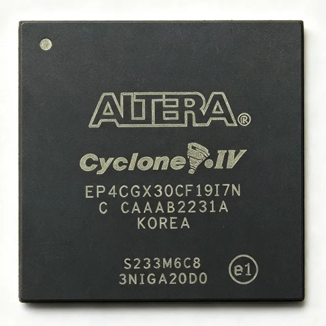
EP4CGX30CF19I7N - Cyclone IV GX FPGA 29K LE 324-FBGA | Intel
EP4CGX30CF19I7N

EP4CGX30CF19I7N - Cyclone IV GX FPGA 29K LE 324-FBGA | Intel

The Intel (formerly Altera) EP4CGX30CF19I7N is a Cyclone IV GX field-programmable gate array (FPGA) offering 29,440 logic elements, 1,105,920 bits of embedded memory, and four integrated 3.125 Gbps transceivers, housed in a 324-ball fine-pitch BGA (FBGA) package with 150 user I/O pins. An FPGA (Field-Programmable Gate Array) is a semiconductor device built around an array of configurable logic blocks (CLBs), programmable interconnect, and hardened I/O resources that engineers can re-program in the field to implement arbitrary digital logic, DSP blocks, or even soft processor cores. FPGAs sit in the broader hierarchy of programmable logic devices (PLDs) -> CPLDs -> FPGAs -> semiconductor ICs, occupying the role of a flexible, parallel-processing alternative to ASICs and microcontrollers for high-throughput, low-latency, or interface-bridging tasks. The Cyclone IV GX family is Intel's low-cost, low-power FPGA line that adds high-speed serial transceiver capability. This variant integrates four full-duplex 3.125 Gbps transceivers (eight channels total), making it suitable for protocols such as PCIe Gen1, Gigabit Ethernet, Serial RapidIO, and CPRI. The device supports up to 150 user I/O across multiple I/O bank voltages and offers 66 18x18 multipliers for DSP workloads. Architecture highlights include a 60 nm low-power process, 1.1V core voltage, four PLLs, 720 Kbits of MLAB memory, and hard memory controllers supporting DDR/DDR2/DDR3 SDRAM, QDRII+ SRAM, and RLDRAM II. The 324-FBGA package operates across the industrial temperature range (-40C to +100C junction) and is suited to cost-sensitive high-volume applications such as industrial imaging, video bridging, and protocol conversion. Typical applications for EP4CGX30CF19I7N include PCI Express endpoint cards, industrial machine vision camera interfaces, motor control and factory automation, software-defined radio front ends, and broadcast video processing. The combination of transceivers and abundant DSP blocks makes it a common drop-in for designs that require protocol bridging alongside signal processing. When designing with this device, pay close attention to transceiver reference clock routing and PCB stack-up - the 3.125 Gbps channels demand controlled-impedance differential traces and continuous reference planes. Quartus II / Quartus Prime design software is required for synthesis, place-and-route, and bitstream generation. This page synthesizes Intel distributor pricing, drop-in same-package variants from the Cyclone IV GX family, and practical PCB/transceiver design notes not consolidated in any single distributor listing.

USD $76.40 联系我们