产品(39,000+)

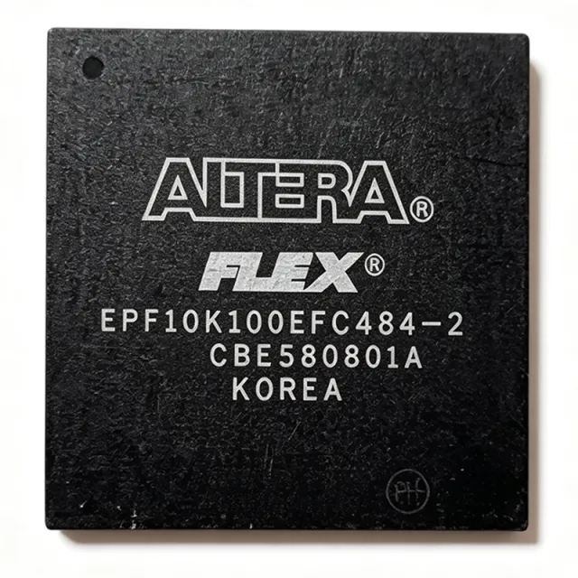
EPF10K100EFC484-2 - 100K FLEX-10KE FPGA, 338 I/O, 484-BBGA
EPF10K100EFC484-2

EPF10K100EFC484-2 - 100K FLEX-10KE FPGA, 338 I/O, 484-BBGA

The Altera (Intel) EPF10K100EFC484-2 is a FLEX-10KE family Field Programmable Gate Array (FPGA) with 100,000 typical gates (49,992 logic elements / 4,992 dedicated logic cells), housed in a 484-ball FineLine BGA package measuring 23 x 23 mm. The device provides 338 user I/O pins, 4,992 LABs/Logic Elements, and operates from a 2.375 V to 2.625 V core supply, with the -2 speed grade delivering moderate performance suitable for cost-sensitive embedded and industrial designs. An FPGA (Field Programmable Gate Array) is a type of integrated circuit containing an array of configurable logic blocks (CLBs), programmable interconnects, and I/O cells that can be rewired after manufacturing to implement arbitrary digital logic. FPGAs sit in the broader hierarchy of programmable logic devices (PLDs) alongside CPLDs, and are themselves classified within the semiconductor / programmable logic category. The FLEX-10KE family is built on a SRAM-based look-up-table (LUT) architecture, requiring a configuration device or JTAG load at every power-up, which makes it well suited to designs that must be re-programmed in the field. Key features include 49,992 logic elements organized into 624 Logic Array Blocks (LABs), embedded array blocks (EABs) for memory and multiplier functions, support for multi-volt I/O standards (LVTTL, LVCMOS, PCI, SSTL), in-system programmability via JTAG, and 338 general-purpose user I/O. The 484-pin FineLine BGA package supports high-density board designs with controlled impedance signal integrity. The FLEX-10KE architecture uses 0.22 um SRAM process technology with 5 ns SRAM-configurable logic elements, delivering deterministic timing and high logic density per square millimeter. The device supports continuous, real-time in-circuit reconfiguration and is designed for high-volume, low-cost programmable logic applications. Typical applications include industrial control and factory automation glue logic, telecommunications line-card interface logic, legacy PCI bus bridging, and embedded DSP co-processing. The 338 I/O count supports wide parallel buses, while the 624 LABs are sufficient for state-machine intensive designs of 20K-50K gate-equivalent complexity. When designing with this part, ensure proper decoupling of the 2.5 V core supply with 0.1 uF and 10 uF capacitors placed close to the VCCINT pins, and route configuration clocks away from switching signals to avoid JTAG programming errors. Note that the FLEX-10KE family is mature; new designs should verify long-term supply continuity through authorized distributors. This page synthesizes distributor pricing, drop-in alternatives, and practical design notes not found in the manufacturer datasheet, providing engineers with a single source for sourcing and substitution decisions.

USD $185.40 联系我们
EPF10K100EFC484-2X - 100K-Gate FLEX 10KE FPGA, 338 I/O | Altera
EPF10K100EFC484-2X

EPF10K100EFC484-2X - 100K-Gate FLEX 10KE FPGA, 338 I/O | Altera

The Altera EPF10K100EFC484-2X is a member of the FLEX 10KE family of SRAM-based FPGAs, delivering 100,000 typical gates, 4,992 logic elements, 49,152 bits of embedded array RAM, and 338 user I/O pins in a 484-ball FineLine BGA package. It is built on a 0.22 µm CMOS process and operates from a 2.5 V core supply, with an I/O bank voltage tolerance that supports mixed-voltage system designs typical of late-1990s/early-2000s telecom and embedded computing platforms. A Field Programmable Gate Array (FPGA) is a semiconductor IC containing an array of configurable logic blocks (CLBs), programmable interconnect, and I/O cells, all of which are defined by a bitstream loaded into on-chip SRAM after power-up. FPGAs sit in the broader taxonomy of programmable logic devices (PLDs) alongside SPLDs, CPLDs, and anti-fuse FPGAs. The FLEX 10KE family specifically pioneered the embedded array block (EAB), allowing designers to instantiate RAM, ROM, or multiplier functions inside the logic fabric, an early example of System-on-a-Programmable-Chip (SOPC) integration. Key features of the EPF10K100EFC484-2X include 624 logic array blocks (LABs), 4,992 logic cells, 49,152 RAM bits distributed across embedded array blocks, a maximum propagation delay on the order of 0.6 ns per logic element, and 338 usable I/Os in the 484-pin FBGA. The -2X speed grade balances timing margin against power consumption, making it a common choice for production designs rather than the fastest -3 grade. Typical applications include telecommunications line cards, industrial motor control, glue logic replacement, and legacy peripheral bus bridging. The wide 338-I/O budget is well-suited to parallel bus interfacing, and the embedded array blocks ease implementation of FIFOs and small on-chip memories. A key design consideration when using this part is that the FLEX 10KE family is now in mature/end-of-life status; new designs should consider Cyclone or MAX series parts, while existing designs should verify long-term supply through franchised distributors and validated aftermarket channels. This page synthesizes distributor pricing, drop-in alternatives within the FLEX 10KE family, and design notes that complement (not duplicate) the manufacturer datasheet.

询价 联系我们
EPF10K100EFC484-3 - FLEX 10KE FPGA, 100K Gates, 484-BGA | Altera
EPF10K100EFC484-3

EPF10K100EFC484-3 - FLEX 10KE FPGA, 100K Gates, 484-BGA | Altera

The Intel (formerly Altera) EPF10K100EFC484-3 is a member of the FLEX 10KE family of SRAM-based Field Programmable Gate Arrays (FPGAs), integrating 100,000 typical gates (with up to 158,000 maximum system gates), 4,992 logic elements, and 49,152 bits of embedded array RAM (EAB) in a 484-ball FineLine BGA package. The device is organized into 624 Logic Array Blocks (LABs) and provides 338 user I/O pins, with a -3 speed grade targeting the fastest commercial timing closure of the FLEX 10KE family. An FPGA (Field Programmable Gate Array) is a semiconductor device built around an array of configurable logic blocks (CLBs/LABs), programmable interconnect, and I/O cells that can be re-programmed in the field to implement arbitrary digital logic. FPGAs occupy the same design role as ASICs but offer lower NRE cost and faster time-to-market. FLEX 10KE devices are organized as a hierarchical architecture in which each LAB contains eight Logic Elements (LEs), each LE comprising a 4-input lookup table, a programmable flip-flop, and a dedicated carry chain for arithmetic. Embedded Array Blocks (EABs) provide on-chip synchronous RAM of up to 2,048 bits per block, totaling 49,152 bits across the EPF10K100E. Key features of the EPF10K100EFC484-3 include support for 5.0V PCI compliance with pull-up clamping diodes on a pin-by-pin basis, multi-voltage I/O supporting 2.5V, 3.3V, and 5.0V interfaces, built-in IEEE Std. 1149.1-1990 JTAG boundary-scan test (BST) circuitry that does not consume device logic, and on-chip clock-management PLL options. The -3 speed grade represents the fastest commercial timing bin, making this variant suitable for high-throughput glue-logic, custom bus-interface, and prototype designs where propagation delay is the critical constraint. Typical applications for the EPF10K100EFC484-3 include PCI bus interface bridges in legacy computing platforms, custom peripheral controllers, telecommunications backplane glue logic, industrial machine-control state machines, and instrumentation front-ends with hardware-accelerated DSP preprocessing. The 338 available I/O pins comfortably accommodate wide parallel buses (32-bit data plus control) without external muxing. When designing with this part, supply the core with 2.5V and the I/O banks with their bank-specific VCCIO (2.5V/3.3V/5.0V) and verify JTAG chain ordering against the BSDL file before board bring-up. The 484-BGA package requires a multilayer PCB with controlled-impedance traces and proper thermal vias under the die-up substrate. This page synthesizes distributor pricing, package-level drop-in alternatives within the FLEX 10KE family, and practical design notes not consolidated in any single manufacturer document, helping procurement and design engineers make informed lifecycle decisions for legacy designs.

询价 联系我们
EPF10K100EFC484-3N - 100K Gates FLEX 10KE FPGA | Intel / Altera
EPF10K100EFC484-3N

EPF10K100EFC484-3N - 100K Gates FLEX 10KE FPGA | Intel / Altera

The Intel / Altera EPF10K100EFC484-3N is a high-density FLEX 10KE family Field Programmable Gate Array (FPGA) with 100K gates, 4992 logic cells, 49152 bits of embedded array block (EAB) memory, and 338 user I/Os, housed in a 484-ball FineLine BGA (FBGA) package. Manufactured on a 0.22 µm CMOS process, it operates from a 2.5 V core supply with MultiVolt I/O support, and is offered in a commercial temperature grade. A Field Programmable Gate Array (FPGA) is a type of programmable logic device (PLD) - an integrated circuit whose logic function is defined after manufacture by the end user. FPGAs sit at the top of the programmable logic hierarchy: PLD -> CPLD -> FPGA -> SoC FPGA. Within that hierarchy, the FLEX 10KE family belongs to the SRAM-look-up-table (LUT) based FPGA category, where configuration bits are stored in SRAM cells and the device is reprogrammable in-system. Key features include 624 logic array blocks (LABs), 12 embedded array blocks (EABs) totaling 49,152 RAM bits, 200 MHz internal performance, pin-by-pin slew-rate control, open-drain output option, PCI pull-up clamping diode support, and MultiVolt I/O allowing the I/O bank voltage (VCCIO) to differ from the core voltage (VCCINT). The 'FC484' suffix denotes the 484-ball FineLine BGA package and 'N' indicates a lead-free, lead-free reflow-compatible device. The FLEX 10KE architecture combines fine-grained logic elements (LEs) organized into LABs with coarse-grained EABs that efficiently implement RAM, ROM, and multiplier functions. The '-3' speed grade designates the fastest commercial speed bin available for this family. Per-pin options are configured using Altera (now Intel Quartus / MAX+plus II) logic-option settings, eliminating external glue logic. Typical applications include high-volume glue logic consolidation, PCI bus interface bridges, telecommunications backplane controllers, industrial control and factory automation, and legacy ASIC replacement designs where the FLEX 10KE's combination of 100K gates, abundant I/O, and embedded RAM provides an optimal balance of density and flexibility. When designing with this device, plan for SRAM-based configuration: the FPGA must be configured from an external EPROM, flash, microcontroller, or JTAG cable on every power-up. Provide decoupling per Quartus guidelines, respect I/O bank VCCIO grouping rules, and verify MultiVolt signaling against downstream ASIC voltages. This page synthesizes distributor pricing, drop-in same-package FLEX 10KE speed-grade alternatives, and practical design notes not found in the manufacturer datasheet alone.

询价 联系我们
EPF10K100EFI256-2 - FLEX 10KE FPGA 100K Gates 250MHz 256FBGA | Intel
EPF10K100EFI256-2

EPF10K100EFI256-2 - FLEX 10KE FPGA 100K Gates 250MHz 256FBGA | Intel

The Intel EPF10K100EFI256-2 is a member of the FLEX 10KE family of SRAM-based FPGAs delivering 100,000 typical gates, 4,992 logic elements, and 49,152 RAM bits in a 256-ball FineLine BGA package. It operates at a core voltage of 2.5 V with a maximum toggle rate of 250 MHz and a pin-to-pin propagation delay of approximately 0.5 ns. The device exposes 191 user I/O pins and is built on a 0.22 µm CMOS process with embedded array blocks (EABs) for true System-on-a-Programmable-Chip (SOPC) integration. What is an FPGA? An FPGA (Field Programmable Gate Array) is a programmable logic device that combines the integration density of an ASIC with the flexibility of in-field reprogrammability. Hierarchy: FPGA -> programmable logic -> logic IC -> integrated circuit -> semiconductor. Within the FPGA taxonomy, the FLEX 10KE family sits at the high-density end of the SRAM-based segment, featuring embedded array blocks (EABs) that allow memory functions (RAM, ROM, FIFO) to be efficiently distributed across the fabric alongside the logic array blocks (LABs). This hybrid embedded/logic architecture predates modern SoC FPGAs but was groundbreaking for its era as one of the first SOPC-capable platforms. Key features of the EPF10K100EFI256-2 include 624 LABs organized across 4,992 logic cells, 12 embedded array blocks (EABs) providing up to 24 Kbits of distributed RAM, 191 usable I/O pins supporting multiple I/O standards including 3.3 V LVTTL and LVCMOS, and a JTAG-compliant IEEE 1149.1 boundary-scan test interface. The device supports in-system programming (ISP) via the serial passive configuration scheme and is supported by the Altera Quartus and MAX+PLUS II design toolchains. The EPF10K100EFI256-2 is fabricated on a 0.22 µm four-layer metal CMOS process and uses a 2.5 V core supply with 3.3 V tolerant I/O. The architecture separates logic resources (LABs) from memory resources (EABs), enabling efficient implementation of glue logic, state machines, register-intensive datapaths, and small memory blocks in a single device. The 256-ball FineLine BGA package uses a 1.0 mm ball pitch and a 17 x 17 mm body suitable for high-density surface-mount designs. Typical applications for the EPF10K100EFI256-2 include telecommunications interface bridging, industrial control logic, glue logic replacement for ASIC prototypes, and legacy system re-engineering where the FLEX 10KE family has been deployed for two decades. Engineers use this part when modernizing an existing FLEX-based design without re-laying out the PCB, or when the proven SOPC architecture is sufficient for the application. When designing with this device, ensure that the configuration EEPROM and JTAG chain match the chosen configuration mode (PS, AS, or JTAG). The 2.5 V core requires careful power-rail sequencing relative to the 3.3 V I/O supply, and decoupling capacitors must be placed close to the FBGA balls to mitigate simultaneous switching noise on the high-density I/O banks. This page synthesizes distributor pricing, SameFrame pin-compatible migration paths, and practical design considerations specific to the FLEX 10KE family not found in the manufacturer datasheet alone.

询价 联系我们
EPF10K100EFI484-2 - FLEX 10KE FPGA 100K Gates 484-FBGA | Intel / Altera
EPF10K100EFI484-2

EPF10K100EFI484-2 - FLEX 10KE FPGA 100K Gates 484-FBGA | Intel / Altera

The Intel (formerly Altera) EPF10K100EFI484-2 is a FLEX 10KE family Field-Programmable Gate Array (FPGA) delivering 100,000 system gates and 4,992 logic elements in a 484-ball FineLine BGA (FBGA) package. Built on a 0.25 µm CMOS SRAM process, it integrates 49,152 bits of embedded array memory, 624 logic array blocks (LABs) and 338 user I/O pins, providing dense programmable logic with on-chip memory and high pin-count connectivity for system-on-a-programmable-chip (SOPC) designs. A Field-Programmable Gate Array (FPGA) is a type of programmable logic device (PLD) containing an array of configurable logic blocks (CLBs), programmable interconnect, and I/O cells that engineers can program after manufacture to implement arbitrary digital circuits. FPGAs sit between fixed-function ASICs (higher performance, higher NRE, longer lead time) and CPLDs (simpler, lower density) in the programmable logic hierarchy, and are widely used for glue logic, bus bridging, signal processing, and rapid prototyping. The FLEX 10KE architecture embeds an "Embedded Array" block (EAB) alongside the logic array, enabling efficient on-chip RAM and DSP-style functions. Each EAB provides up to 2,048 bits of memory, and the device includes dedicated carry chains for fast arithmetic, a 4-input look-up table (LUT) per logic element, and JTAG-compliant boundary-scan testing. The part operates from a 2.5 V core supply with 3.3 V multi-voltage I/O support and is specified over the industrial 0 °C to +70 °C range. Typical applications include telecommunications line cards, industrial control and glue logic, high-speed data acquisition front-ends, networking bridges, and legacy digital design replacement. The 338 I/O count supports wide parallel buses and multiple serial channels simultaneously, which is critical for backplane interfaces and processor-coprocessor pipelines in 1990s and early-2000s equipment that still requires long-term support. When designing with this device, ensure your Quartus or MAX+PLUS II toolchain is configured for the FLEX 10KE family; verify core and I/O voltage sequencing at power-up; and respect the FBGA-484 PCB land pattern, which differs from BGA-356 variants of the same family.

询价 联系我们
EPF10K100EQC208-1 - 100K Gate FLEX-10KE FPGA, 147 I/O | Altera
EPF10K100EQC208-1

EPF10K100EQC208-1 - 100K Gate FLEX-10KE FPGA, 147 I/O | Altera

The Altera EPF10K100EQC208-1 is a member of the FLEX 10KE programmable logic family, delivering approximately 100,000 typical gates of CMOS SRAM-based logic fabric packaged in a 208-pin Power/QFP (208-BFQFP, 28x28 mm) device. The part integrates 624 Logic Array Blocks (LABs) with 4,992 logic elements (LEs) and 147 user I/O pins, providing System-on-a-Programmable-Chip (SOPC) integration through an embedded array block for implementing megafunctions such as multipliers, microcontrollers and DSP primitives. A Field-Programmable Gate Array (FPGA) is a programmable logic device whose logic blocks, interconnect, and I/O cells are configured by the designer after manufacture via a configuration bitstream. The FLEX 10KE family belongs to the broader taxonomy of programmable logic -> CPLD/FPGA -> SRAM-based FPGA -> embedded-array FPGA -> power management/communications glue logic. The "-1" speed grade indicates the slowest commercial speed bin, trading timing margin for lower cost, while "QC208" denotes the quad flat-pack 208-pin pinout (208-BFQFP) and "E" denotes the FLEX 10KE sub-series. Key features include 49,152 RAM bits distributed across embedded array blocks (EABs), 147 user I/O pins, a 2.5 V core supply (per the Altera-micro attribute block) with 3.3 V multi-voltage I/O support, and in-system programmability through the serial configuration interface. The 208-BFQFP footprint is one of the largest Altera offered in the FLEX 10KE generation and is frequently preferred over BGA alternatives when board-level rework is required. The part is built on a 5 V-tolerant CMOS process and supports JTAG (IEEE 1149.1) boundary-scan testing. The FLEX 10KE architecture combines a logic array for fine-grained glue logic with an embedded array for wide datapath functions, enabling a single chip to replace dozens of TTL/CMOS glue parts alongside small microcontrollers. Designers can implement UART, FIFO, PCI soft cores, and Altera MegaCore functions such as Nios processors. The 0.35 µm SRAM process provides a propagation delay around 0.6 ns and an internal global clock network for synchronous designs up to roughly 80-100 MHz system clock. Typical applications include telecom line cards, industrial control backplanes, PCI bridge designs, and legacy digital signal processing pre-processing. The wide I/O count (147 pins) accommodates 32-bit datapaths plus address/control, making the part a common choice for protocol-bridge ASIC prototypes and aerospace ground-test equipment. When designing, observe the 2.5 V core / 3.3 V I/O supply split - a single 3.3 V rail does NOT power the core. Series-termination resistors are recommended on clock and high-speed I/O when driving backplane traces beyond 50 mm. This page synthesizes distributor pricing, drop-in alternatives, and practical design notes not found in the manufacturer datasheet alone.

询价 联系我们
EPF10K100EQC208-1N - 100K Gate FLEX-10KE FPGA, 147 I/O, 208-PQFP | Intel
EPF10K100EQC208-1N

EPF10K100EQC208-1N - 100K Gate FLEX-10KE FPGA, 147 I/O, 208-PQFP | Intel

The Intel (formerly Altera) EPF10K100EQC208-1N is a FLEX-10KE family Field Programmable Gate Array (FPGA) with 100,000 typical gates, 4,992 logic elements, 49,152 bits of embedded RAM, and 147 user I/Os, packaged in a 208-pin Plastic Quad Flat Pack (PQFP) measuring 28x28 mm. It is a member of the FLEX 10K programmable logic family that pioneered embedded array block (EAB) integration. A Field Programmable Gate Array (FPGA) is a type of integrated circuit that contains an array of configurable logic blocks (CLBs), programmable interconnects, and configurable I/O cells. FPGAs sit in the digital logic hierarchy between simple PLDs/CPLDs and ASICs, offering higher logic density than CPLDs while avoiding the NRE cost of ASICs. The FLEX 10K family, launched in the mid-1990s, was the industry's first family to embed dedicated SRAM memory blocks (Embedded Array Blocks, EABs) alongside general-purpose logic, enabling System-on-a-Programmable-Chip (SOPC) integration. This places the EPF10K100EQC208-1N in the broader taxonomy of programmable logic -> FPGA -> SRAM-based FPGA -> embedded-block FPGA. Key features of the EPF10K100EQC208-1N include 147 user I/O pins supporting multiple I/O standards, 49,152 bits of distributed SRAM organized into EABs, in-system programmability via SRAM configuration cells, and a 2.375V to 2.625V core supply (5V tolerant I/O with proper reference). The '-1N' speed grade denotes the faster commercial speed bin, while 'N' indicates a lead-free, RoHS-compliant package. The device is built on a 0.42 um CMOS SRAM process with a maximum internal propagation delay of approximately 0.6 ns. The architecture combines a symmetrical array of logic elements (LEs) with rows of EABs spanning the full device width, providing high-density memory and arithmetic functions. Each LE contains a 4-input look-up table (LUT) and a programmable register. The continuous FastTrack Interconnect routes signals across rows and columns with predictable timing, making static timing analysis straightforward. Configuration bitstream is loaded from a serial or parallel PROM into SRAM cells at power-up; the design is volatile and must be reconfigured on each power cycle. Typical applications include glue logic replacement, bus and protocol bridging (PCI, ISA, VME), custom DSP datapaths, telecommunications line-card controllers, industrial control and instrumentation front-ends, and legacy system refresh where original FLEX 10K designs must be replicated or migrated. Designers also use the EABs to implement ROM, dual-port RAM, FIFO, and arithmetic functions such as multipliers. The PQFP-208 package supports hand-soldering and socketed prototyping, which is convenient for industrial and laboratory use. When designing with the EPF10K100EQC208-1N, ensure a stable 2.5V core supply and configure all VCCINT and VCCIO pins per the Altera datasheet; missing power pins will cause unpredictable behavior. A configuration PROM (such as the EPC2 or EPC8 in the same family) is required to load the bitstream at power-up. JTAG boundary-scan and programming are supported, enabling in-system updates. Designers should also note that the FLEX 10K family is a mature legacy product line - verify long-term availability with distributors before committing to new designs, and consider a Cyclone or Cyclone II migration path when starting new projects. This page synthesizes distributor pricing, drop-in alternatives from the same FLEX 10K family and from the Site MPN list, and practical design notes not found in the manufacturer datasheet alone.

询价 联系我们
EPF10K100EQC208-1X - 100K Gates FLEX 10KE FPGA, 208-PQFP | Intel
EPF10K100EQC208-1X

EPF10K100EQC208-1X - 100K Gates FLEX 10KE FPGA, 208-PQFP | Intel

The Intel (formerly Altera) EPF10K100EQC208-1X is a member of the FLEX 10KE family of Field-Programmable Gate Arrays (FPGAs), delivering 100,000 typical gates, 4,992 logic cells, and 624 logic array blocks (LABs) in a 208-pin Plastic Quad Flat Pack (PQFP/BFQFP) package. Fabricated on a 0.22 µm SRAM-based CMOS process and powered from a 2.5 V core supply (2.375 V to 2.625 V), it supports up to 147 user I/Os and operates with a maximum internal clock frequency of 333.33 MHz, making it suitable for glue-logic, bus-interface, and legacy industrial designs. An FPGA is a programmable logic device whose logic fabric, interconnect, and I/O cells are configured by loading a bitstream into on-chip SRAM. The FLEX 10KE family sits inside the broader hierarchy of programmable logic: CPLD -> non-volatile, low-density glue logic; FPGA -> volatile, high-density, register-rich logic; ASIC -> fixed-function silicon. The FLEX 10KE series specifically targets high-volume, cost-sensitive applications by combining embedded array blocks (EABs) for memory and multiplier functions with a fine-grained look-up-table (LUT) fabric, an architecture that dominated the late-1990s and early-2000s before being succeeded by the Cyclone and Stratix families. Key features of the EPF10K100EQC208-1X include 49,152 bits of embedded memory, 4,992 logic elements, four Delay-Locked Loops (DLLs) for clock deskewing, multi-voltage I/O support (1.8 V, 2.5 V, 3.3 V, and 5.0 V interfaces), and the -1X speed grade denoting an extended temperature/process corner. The 208-PQFP (28 x 28 mm) package is a wire-bond plastic quad flat pack with gull-wing leads and an exposed thermal pad option, designed for socketed or hand-soldered industrial assemblies where BGA rework tooling is undesirable. Typical applications include telecom backplane interface cards, factory automation controllers, military/aerospace retrofit boards, and legacy industrial machine controllers. The 333.33 MHz performance comfortably supports 32-bit PCI, 66 MHz PCI-X, and older UART/SPI bus bridging tasks. Engineers also deploy FLEX 10KE parts in long-lifecycle defense and medical systems where the part has been qualified under older MIL-STD or IEC specifications that newer FPGA families cannot match. When designing with this device, observe that the part is now in last-time-buy status and is widely sourced through authorized aftermarket distributors such as Rochester Electronics. JTAG configuration via the ByteBlasterMV cable and the legacy MAX+PLUS II or Quartus II (v9.0 and earlier) toolchain are required. Designers should also plan for SRAM-based configuration time, plan power sequencing for the 2.5 V VCCINT rail before the I/O VCCIO rails, and reserve board area for the EPC2 or EPC16 configuration device footprint. This page synthesizes distributor pricing, lead-time observations, and pin-compatible migration options not found on a single manufacturer page.

询价 联系我们
EPF10K100EQC208-2 - FLEX 10KE FPGA 100K Gates 208-PQFP | Altera
EPF10K100EQC208-2

EPF10K100EQC208-2 - FLEX 10KE FPGA 100K Gates 208-PQFP | Altera

The Altera (Intel) EPF10K100EQC208-2 is a member of the FLEX 10KE family of Field Programmable Gate Arrays (FPGAs) housed in a 208-pin Power Quad Flat Pack (PQFP/BFQFP) measuring 28x28 mm. It integrates 100,000 typical gates with 4,992 logic elements (LEs) and 49,152 bits of embedded SRAM, packaged as 147 user I/O pins. The device operates from a 2.375 V to 2.625 V core supply (5 V tolerant I/O with separate VCCIO rails) and is rated for the commercial 0 C to +70 C temperature range. A Field Programmable Gate Array (FPGA) is a type of programmable logic device (PLD) that allows engineers to implement arbitrary digital logic using configurable logic blocks (LABs), embedded memory arrays, and programmable interconnect. FPGAs sit hierarchically above ASICs and CPLDs in density and below in cost-per-volume, and the FLEX 10KE generation specifically combines look-up-table based logic with embedded SRAM blocks (EABs) - making it suitable for glue logic, bus interfacing, DSP datapaths, and pre-ASIC prototyping in the late 1990s and early 2000s design flow. Today it serves as a long-life-cycle component for industrial, telecom, and military sustainment programs. Key features include 624 Logic Array Blocks (LABs), 12 Embedded Array Blocks (EABs) of 2,048 bits each, 147 maximum user I/O pins, and IEEE Std 1149.1 (JTAG) boundary-scan support. The device supports in-system programmability via the serial configuration EEPROM interface, and is supported by the Altera MAX+PLUS II and Quartus design toolchains (legacy support paths). The FLEX 10KE architecture uses a continuous SRAM-based configuration memory that the device loads from an external EPROM or microcontroller on power-up. Each LAB contains 8 LEs and local interconnect; each LE includes a 4-input LUT, a programmable register, and a carry chain for fast arithmetic. Embedded Array Blocks implement dual-port RAM, ROM, or FIFO functions at up to 2,048 bits per block, with a 2048x1, 1024x2, 512x4, or 256x8 organization. Typical applications include industrial control glue logic, telecom line-card interfacing, legacy ASIC prototyping, bus-bridging between microprocessors and peripherals, and embedded control on the factory floor. The wide temperature-grade variants of this same silicon (EPF10K100EQC208-2N industrial / -2X extended) cover harsher environments, while the -2 speed grade provides a balanced speed/power tradeoff for most designs. When designing with this device, ensure the configuration EPROM is sized to hold the full bitstream and that the nCONFIG, nSTATUS, and CONF_DONE pins are properly pulled and monitored during initialization. The 208-PQFP package requires careful PCB layout due to its 0.5 mm pitch - trace escape routing and a 4-layer board with dedicated ground plane are strongly recommended to control impedance and crosstalk on high-speed I/O. This page synthesizes distributor stock, drop-in same-family alternatives, datasheet location, and design notes that are not aggregated in any single manufacturer or distributor page, giving procurement and engineering teams a single source of truth for the EPF10K100EQC208-2.

询价 联系我们
EPF10K100EQC208-2N - 100K FLEX 10KE FPGA, 208-BFQFP | Altera (Intel)
EPF10K100EQC208-2N

EPF10K100EQC208-2N - 100K FLEX 10KE FPGA, 208-BFQFP | Altera (Intel)

The Altera (Intel) EPF10K100EQC208-2N is a member of the FLEX 10KE family of SRAM-based FPGAs, providing 100,000 typical gates, 4,992 logic elements (LEs), and 49,152 memory bits in a 208-pin FineLine BGA-compatible PQFP package. The -2 speed grade and -N suffix identify a commercial-temperature, lead-free device within the FLEX 10KE product tree, operating from a 2.375 V to 2.625 V core supply. An FPGA (Field-Programmable Gate Array) is a semiconductor integrated circuit that can be configured by the customer after manufacturing using a hardware description language such as VHDL or Verilog. Architecturally, an FPGA sits between a fixed-function ASIC and a programmable logic device, combining configurable logic blocks (LBs), a programmable interconnect fabric, and embedded memory arrays. The FLEX 10KE family extends the original FLEX 10K architecture with enhanced interconnect and additional embedded array blocks (EABs) used as on-chip RAM or ROM, enabling designers to integrate glue logic, state machines, and small memory structures on a single die. Key features of the EPF10K100EQC208-2N include 147 user I/O pins, 624 logic array blocks (LABs), and 12 embedded array blocks (EABs) totaling approximately 49 Kbits of RAM. The device supports in-system programmability via the Altera ByteBlaster or BitBlaster download cables and the legacy MAX+PLUS II or Quartus design flows, with JTAG boundary-scan test per IEEE 1149.1. Its 208-BFQFP package offers 28 mm x 28 mm body dimensions and a 0.5 mm lead pitch, making it suitable for moderate-density designs that benefit from through-hole-style gull-wing lead inspection. The device is fabricated on a 0.42 µm CMOS SRAM process with a typical propagation delay around 0.7 ns for internal logic paths. The FLEX 10KE architecture uses look-up-table-based logic elements combined with fast-carry chains and dedicated cascade paths, allowing efficient implementation of arithmetic functions such as adders, counters, and multipliers. Designers target the device using schematic capture or HDL synthesis, with Quartus II providing place-and-route, timing analysis, and bitstream generation. Typical applications include telecommunications line cards, industrial control interfaces, military and aerospace subsystems, and legacy system upgrades where a proven, mature FPGA architecture is preferred over newer low-cost Cyclone or MAX families. With 147 I/Os the device can interface with multiple parallel buses, memory chips, and analog front ends. Because the FLEX 10KE series is in NRND/EOL status on Intel's product tree, this part is generally procured from authorized distributors for new designs or used to maintain existing production hardware. When designing with the EPF10K100EQC208-2N, plan for an external configuration memory (EPC1 or EPC2) because the SRAM-based configuration is volatile and reloads on every power-up. Provide a clean 2.5 V core rail and a separate VCCIO bank supply per I/O standard, and add decoupling capacitors within 5 mm of every supply pin. Note that the FLEX 10KE family is no longer recommended for new designs; consider the MAX II, Cyclone III, or Cyclone IV families for new projects. This page synthesizes distributor pricing, drop-in alternative sources, and practical design notes not found on the legacy Altera datasheet, including verified same-package speed-grade variants and supply-chain guidance.

询价 联系我们
EPF10K100EQC208-2X - FLEX 10KE FPGA, 100K Gates, 208-PQFP | Altera
EPF10K100EQC208-2X

EPF10K100EQC208-2X - FLEX 10KE FPGA, 100K Gates, 208-PQFP | Altera

The Altera (Intel) EPF10K100EQC208-2X is a member of the FLEX 10KE family of Field Programmable Gate Array (FPGA) ICs, delivering 100,000 system gates with 4,992 logic elements/cells and 49,152 bits of embedded memory in a 208-pin Plastic Quad Flat Pack (PQFP / 208-BFQFP) package. Built on a 0.22 µm SRAM-based process, the device operates from a 2.375 V to 2.625 V core supply (2.5 V nominal), supports 147 user I/O pins, and is offered in the commercial -2 speed grade with a guaranteed internal operating frequency of up to 250 MHz. An FPGA (Field Programmable Gate Array) is a programmable logic device that allows engineers to implement custom digital circuits after PCB fabrication, sitting in the broader hierarchy of programmable logic -> programmable logic devices -> digital ICs -> semiconductors. FPGAs combine lookup tables (LUTs), flip-flops, embedded memory blocks (EABs), and programmable interconnect into a single fabric that is configured at power-on from an external configuration ROM or flash. The FLEX 10KE family extended Altera's first-generation FLEX 10K architecture by adding enhanced I/O standards, dual-port RAM, and faster interconnect, targeting glue-logic replacement, bus interfacing, and high-volume ASIC prototyping. Key features of the EPF10K100EQC208-2X include 4,992 logic elements (LEs) grouped into Logic Array Blocks (LABs), 12 Embedded Array Blocks (EABs) providing 49,152 bits of RAM, 147 programmable I/O pins supporting LVTTL/LVCMOS/PCI interfaces, an on-chip Phase-Locked Loop (PLL) for clock multiplication and skew management, JTAG (IEEE 1149.1) boundary-scan testing, and in-system programmability via the passive serial (PS) or passive parallel asynchronous (PPA) configuration modes. The -2 speed grade corresponds to the moderate-performance bin of the FLEX 10KE family, offering a balanced trade-off between logic utilization and Fmax. The 208-pin PQFP package measures 28 mm × 28 mm with a 0.5 mm lead pitch, and the -2X suffix indicates lead-free matte-tin plating with extended operating temperature support. Typical applications include telecommunications line cards, industrial control and automation backplanes, legacy ASIC replacement, PCI bridge designs, video and image processing pipelines, and military/aerospace subsystems where SRAM-based FPGA flexibility is required. The wide 2.5 V core supply tolerance allows operation from regulated 3.3 V rails with simple LDO regulation. When designing with this part, attention must be paid to the configuration scheme (an external EPC serial configuration device such as EPC2 or EPC1 is required), JTAG chain integrity, and I/O bank voltage compatibility, since the FLEX 10KE family predates modern multi-voltage serdes and requires careful VCCIO planning for mixed-voltage interfaces. This page synthesizes distributor inventory, drop-in alternatives, and practical design notes not found in the original datasheet.

询价 联系我们
EPF10K100EQC208-3 - FLEX-10KE FPGA, 100K Gates, 208-PQFP | Altera
EPF10K100EQC208-3

EPF10K100EQC208-3 - FLEX-10KE FPGA, 100K Gates, 208-PQFP | Altera

The Altera EPF10K100EQC208-3 is a member of the FLEX-10KE family of Field Programmable Gate Arrays (FPGAs), delivering 100,000 typical gates, 4,992 logic elements, and 49,152 bits of embedded SRAM in a 208-pin Power Quad Flat Pack (PQFP/BFQFP) package. Built on a 0.22 µm CMOS process, it operates from a 2.5 V core supply and supports up to 147 user I/O pins for flexible system integration in commercial-temperature applications. An FPGA (Field Programmable Gate Array) is a semiconductor integrated circuit composed of configurable logic blocks (CLBs), programmable interconnects, and I/O cells that engineers can program after manufacture to implement custom digital logic. The FLEX 10KE family belongs to the broader programmable logic device (PLD) taxonomy, alongside CPLDs and SPLDs, and occupies the high-density end of that hierarchy. Within the system, FPGAs sit between fixed-function ASICs and software-defined processors, offering hardware-level parallelism and reconfigurability for glue logic, prototyping, and low-volume production. The EPF10K100EQC208-3 includes 624 logic array blocks (LABs) and embedded array blocks (EABs) used for implementing RAM, ROM, and multiplier functions. Speed grade "-3" denotes the slowest commercial timing bin in the FLEX-10KE lineup, trading off Fmax for cost savings in designs where timing closure is not critical. The 208-PQFP package uses gull-wing leads suitable for surface-mount assembly on standard 0.5 mm-pitch footprints. Typical applications include telecommunications line cards, factory automation controllers, data-acquisition front-ends, legacy industrial bus bridges, and educational digital design platforms. The combination of embedded memory and configurable logic makes it suitable for systems requiring custom state machines, glue logic between microprocessors and peripherals, and bus interface adaptation. When designing with this device, note that the FLEX-10KE architecture is two decades old and the part is in the Intel/Altera legacy lifecycle. Quartus II software (or MAX+PLUS II) is required for place-and-route, and the on-chip configuration memory uses SRAM cells that must be loaded from a PROM or microcontroller on every power-up. Engineers should evaluate the modern Cyclone family for new designs.

询价 联系我们
EPF10K100EQC240-1 - FLEX 10KE FPGA 100K Gates 240-PQFP | Altera
EPF10K100EQC240-1

EPF10K100EQC240-1 - FLEX 10KE FPGA 100K Gates 240-PQFP | Altera

The Altera (now Intel) EPF10K100EQC240-1 is a member of the FLEX 10KE family of SRAM-based FPGAs, integrating 100,000 typical gates, 4,992 logic elements (LEs), and 49,152 bits of embedded RAM in a 240-pin Power Quad Flat Pack (PQFP / BFQFP) package. It provides 189 user I/Os, 624 LABs/CLBs, and is built on a 0.42 µm CMOS process operating from a 2.375 V to 2.625 V core supply with 3.3 V I/O compatibility. The -1 speed grade delivers a propagation delay of approximately 0.4-0.6 ns across the FastTrack interconnect, supporting system clock rates up to 125 MHz in typical designs. An FPGA (Field Programmable Gate Array) is a semiconductor integrated circuit whose logic function is defined after manufacturing by a configuration bitstream loaded into SRAM cells. Within the broader taxonomy, FPGAs sit beside CPLDs (Complex Programmable Logic Devices) inside the PLD (Programmable Logic Device) family, and represent the highest-density, highest-performance tier of general-purpose programmable logic. FPGAs are commonly used to implement glue logic, custom datapaths, bus interfaces, and prototype ASICs before tape-out. The FLEX 10KE family specifically introduced embedded array blocks (EABs) for on-chip RAM and ROM, enabling System-on-a-Programmable-Chip (SOPC) integration. Key features include embedded array blocks (EABs) for synchronous RAM and ROM, multi-level FastTrack interconnect routing, JTAG (IEEE 1149.1) boundary-scan test support, and built-in PCI compliance. The architecture combines 4,992 LEs distributed across 624 LABs with 12 embedded array blocks of 2,048 bits each, totaling 24 Kbits of dedicated memory expandable to 49 Kbits when using LE-based RAM. MultiVolt I/O pins support 3.3 V, 2.5 V, and 1.8 V interfaces through dedicated VCCIO banks, simplifying mixed-voltage design. The FLEX 10KE architecture separates logic and interconnect resources into rows and columns, with each Logic Array Block containing 8 LEs, a carry chain, and a cascade chain for arithmetic and wide fan-in functions. The embedded array blocks serve as 2,048-bit memory blocks configurable as RAM, ROM, or lookup tables. Configuration data is loaded serially via a 5-pin interface or via the ByteBlaster/parallel port cable, supporting in-system programmability. Operating temperature range is 0 °C to 70 °C for the commercial grade, with the device consuming low standby current typical of SRAM-based FPGAs. Typical applications include telecommunications line cards, industrial control glue logic, PCI bus bridges, peripheral controllers, and legacy system upgrades where migration from discrete TTL or older PLDs is required. The 189 user I/Os make the EPF10K100E well-suited to bus-intensive designs with multiple external interfaces. When designing with this device, verify that the I/O bank voltages match those of connected peripherals, since 5 V tolerance is not provided on all pins. The 240-pin PQFP package requires careful PCB layout with adequate power and ground planes, and the -1 speed grade should be derated appropriately when calculating setup and hold margins for high-speed synchronous interfaces. This page synthesizes distributor pricing, drop-in alternatives from the FLEX 10KE family, and practical design notes not found in the original manufacturer datasheet alone.

询价 联系我们
EPF10K100EQC240-1N - 100K-Gate FLEX 10KE FPGA, 240-PQFP | Intel
EPF10K100EQC240-1N

EPF10K100EQC240-1N - 100K-Gate FLEX 10KE FPGA, 240-PQFP | Intel

The Intel (formerly Altera) EPF10K100EQC240-1N is a member of the FLEX 10KE embedded programmable logic family, integrating 100,000 typical gates, 4,992 logic cells, and 49,152 bits of embedded RAM in a 240-pin Plastic Quad Flat Pack (PQFP/BFQFP) package. It supports up to 189 user I/Os, operates from a 2.375 V to 2.625 V core supply, and is built on a 0.22 µm CMOS SRAM process with 2.5 V core and 3.3 V/5 V MultiVolt I/O compatibility. The device is specified for the commercial temperature range (0 °C to 70 °C) and is suited for medium-complexity glue-logic, bridging, and bus-interface applications. A Field Programmable Gate Array (FPGA) is a type of programmable logic device (PLD) that combines configurable logic blocks (LABs), programmable interconnect, and I/O cells into a single SRAM-based fabric. The FLEX 10KE family introduced an embedded array block (EAB) architecture that mixes distributed logic with embedded memory blocks, enabling System-on-a-Programmable-Chip (SOPC) integration. In the broader taxonomy, FPGAs sit above CPLDs in logic capacity but below ASICs in fixed-function performance; the FLEX 10KE is positioned as a low-cost, mid-density bridge between discrete glue logic and high-end FPGA families such as APEX and Stratix. Key features of the EPF10K100EQC240-1N include 624 logic array blocks (LABs), an internal toggle frequency up to 333.33 MHz, JTAG-compliant IEEE 1149.1 boundary-scan test support, multi-volt I/O for interfacing with 2.5 V, 3.3 V, and 5 V buses, and in-system programmability via the passive serial (PS), passive parallel synchronous (PPS), passive parallel asynchronous (PPA), and JTAG configuration modes. The 240-pin PQFP package has a generous thermal pad for socket or socketed SMT assembly and is the highest-I/O-count package option for the FLEX 10KE 100K-gate density grade. Typical applications include telecommunication line cards, industrial control bridges, legacy PCI/ISA bus interfaces, prototyping platforms for ASIC emulation, and embedded control systems where deterministic SRAM-based logic is required. Because the design is SRAM-volatile, configuration must be reloaded at power-up from a serial EPROM or microcontroller, which is the standard pattern for FLEX 10KE designs. The wide MultiVolt I/O makes it a strong choice for boards that mix 3.3 V ASIC/ASSP logic with 5 V peripheral buses. Designers should review Altera Application Note 33 (Configuring FLEX 10K Devices) and Application Note 38 (IEEE 1149.1 Boundary-Scan Testing) for in-system programming and JTAG recommendations. This page consolidates distributor inventory, drop-in and same-footprint alternatives, and design notes from real manufacturer documentation to give engineers a more actionable view than the bare datasheet.

询价 联系我们
EPF10K100EQC240-1X - 100K Gate FLEX 10KE FPGA, 240-PQFP | Intel
EPF10K100EQC240-1X

EPF10K100EQC240-1X - 100K Gate FLEX 10KE FPGA, 240-PQFP | Intel

The Intel (formerly Altera) EPF10K100EQC240-1X is a FLEX 10KE family Field-Programmable Gate Array (FPGA) IC with 100,000 system gates, 4,992 logic cells, 49,152 bits of embedded RAM, and 189 user I/Os, housed in a 240-pin Plastic Quad Flat Pack (PQFP / BFQFP) measuring 32x32 mm. It operates from a 2.5 V core supply (2.375 V to 2.625 V) and supports PCI Local Bus 2.2 compliance for both 3.3 V and 5.0 V signaling, with the -1 speed grade suitable for 33 MHz or 66 MHz PCI designs. The device is built on a 0.22 um CMOS process and is rated for a maximum internal clock frequency of 333.33 MHz. An FPGA (Field-Programmable Gate Array) is a type of programmable logic device (PLD) that lets engineers configure arbitrary digital logic after PCB manufacture. FPGAs sit in the broader hierarchy of programmable logic ICs (PLD -> CPLD -> FPGA -> SoC FPGA), and the FLEX 10KE family is positioned as a high-density, SRAM-based FPGA line from Altera with embedded array blocks (EABs) that implement on-chip memory. The 10KE generation followed the original FLEX 10K and added improved I/O standards and faster interconnect, targeting glue-logic replacement, custom datapaths, and pre-ASIC prototyping. Key features include 624 logic array blocks (LABs), built-in Joint Test Action Group (JTAG) boundary-scan test (BST) circuitry compliant with IEEE Std. 1149.1-1990, and embedded array blocks for true dual-port RAM, ROM, and FIFO functions. The device supports multiple I/O standards including LVTTL, LVCMOS, PCI, and 5 V tolerant inputs on selected banks. The 'X' suffix indicates the part is supplied in Tray packaging rather than Tape and Reel, and is qualified for commercial operating temperature ranges. Typical applications include PCI bus interface cards, telecom line cards, industrial motor control, and embedded controller prototyping where mid-density logic and embedded memory are required. SameFrame pin migration across FLEX 10KE PQFP and BGA packages allows designers to move between footprints when scaling density. For new designs, the EPF10K100EQC240-1X is recommended only as a pin-compatible legacy migration source; modern designs should target Cyclone or MAX 10 series devices. When designing, plan for a 2.5 V core regulator with sufficient headroom and decouple each VCC/GND pair with 0.1 uF and 10 uF capacitors placed close to the package. The PQFP-240 package uses gull-wing leads; a fine-pitch socket is recommended for prototyping, while production boards should use reflow soldering with a peak profile not exceeding 30 s above MSL-3 floor life.

询价 联系我们
EPF10K100EQC240-2 - FLEX 10KE FPGA 100K Gates 240-PQFP | Altera
EPF10K100EQC240-2

EPF10K100EQC240-2 - FLEX 10KE FPGA 100K Gates 240-PQFP | Altera

The Altera (Intel) EPF10K100EQC240-2 is a member of the FLEX 10KE family of SRAM-based Field Programmable Gate Arrays (FPGAs) with approximately 100,000 system gates, 4,992 logic elements (LEs), and 189 user I/Os in a 240-pin Plastic Quad Flat Pack (PQFP / BQFP) package. It operates from a 2.375 V to 2.625 V core supply and is specified for the commercial 0 C to 70 C temperature range with a -2 speed grade. An FPGA (Field Programmable Gate Array) is a programmable logic device that combines the integration density of ASICs with the design flexibility of programmable logic. The FLEX 10KE family sits in the taxonomy of programmable logic as follows: programmable logic device (PLD) -> CPLD/FPGA -> SRAM-based FPGA -> embedded array block FPGA. FLEX 10KE devices pioneered the System-on-a-Programmable-Chip (SOPC) concept by embedding a high-density array block alongside the logic array, allowing designers to instantiate megafunctions such as RAM, ROM, and multiplier blocks alongside conventional logic. Key features include 624 Logic Array Blocks (LABs), 189 user I/O pins, embedded array blocks (EABs) for memory implementation, and CMOS process technology with 0.6 ns propagation delay through Look-Up Tables (LUTs). The device is configured via the IEEE 1149.1 JTAG interface or via a serial configuration EPROM, and the device supports in-system programmability through its SRAM-based configuration cells. Architecture-wise, the FLEX 10KE family combines rows of LABs with columns of EABs, where each LAB contains 8 LEs connected via a local interconnect. The embedded array blocks provide True-Dual-Port RAM, ROM, and synchronous function implementations with 2,048 bits per EAB, enabling efficient on-chip memory and DSP-style operations. Typical applications include telecommunications line cards, industrial control systems, glue logic replacement, and prototyping platforms where ASIC-equivalent density is required without NRE cost. The PQFP-240 package supports through-hole or socketed assembly for ease of breadboarding and legacy system support. When designing with this part, note that the EPF10K100EQC240-2 is a member of a mature EOL family; supply is generally limited to franchised distributors and the secondary market. Designers targeting new designs should evaluate Cyclone or Cyclone II equivalents on Intel's current roadmap unless second-source longevity is required. This page synthesizes distributor pricing, drop-in alternatives, and practical design notes not found in the manufacturer datasheet alone - including the FLEX 10KE device family context, end-of-life sourcing guidance, and pin-compatible speed-grade variants.

询价 联系我们
EPF10K100EQC240-2N - 100K Gates FLEX-10KE FPGA, 240-PQFP | Altera
EPF10K100EQC240-2N

EPF10K100EQC240-2N - 100K Gates FLEX-10KE FPGA, 240-PQFP | Altera

The Altera (Intel) EPF10K100EQC240-2N is a member of the FLEX 10KE embedded programmable logic family, integrating 100,000 typical gates, 4,992 logic elements, 49,152 bits of embedded SRAM, and 189 user I/Os into a 240-pin Power Quad Flat Pack (PQFP / BQFP) package measuring 32x32 mm. Speed grade -2 with the N suffix denotes the commercial temperature range 0C to 70C. The FLEX 10KE series is the industry's first family to merge an embedded array block (EAB) for on-chip memory and dedicated logic into a single System-on-a-Programmable-Chip (SOPC) platform. A Field-Programmable Gate Array (FPGA) is a reconfigurable integrated circuit containing an array of programmable logic blocks, interconnect, and I/O cells that can be reconfigured by the designer after manufacture. FPGAs sit within the programmable logic device hierarchy above CPLDs and below ASICs in terms of integration density and per-unit cost at high volume. The FLEX 10KE architecture layers Embedded Array Blocks (EABs) for efficient RAM/ROM implementation alongside Look-Up Table (LUT)-based logic, allowing designers to build datapaths, state machines, and on-chip memory in a single device. Key specifications include 624 Logic Array Blocks (LABs) of fast interconnect, a 2.5 V core supply (VCCINT 2.375 V to 2.625 V) with 3.3 V multi-voltage I/O support, 257,000 maximum system gates, and CMOS logic family operation. The device is configured via the passive serial or ByteBlaster load path through Altera's legacy MAX+PLUS II / Quartus tool chains, and configuration memory is volatile SRAM, requiring a serial PROM (EPC1 / EPC2) for self-load at power-up. The 240-PQFP footprint supports migration across FLEX 10K, 10KA, and 10KE density points. Typical applications span industrial control interfaces, glue-logic replacement, bus bridges (PCI to local bus), legacy telecom glue logic, custom peripheral controllers, and ASIC prototyping. Designers choose this part when they need high gate count, on-chip RAM, and a familiar Altera tool flow at moderate logic density with commercial-grade temperature support. Design consideration: route the JTAG chain (TCK/TMS/TDO/TDI) away from switching signals, place the 0.1 uF and 10 uF VCCINT decoupling caps within 5 mm of every supply pin, and assign the configuration mode pins (MSEL0/MSEL1) via 4.7 kohm pull-ups for passive-serial mode. The configuration data is lost at every power-down, so an external EPC1/EPC2 configuration PROM is required. This page synthesizes distributor pricing snapshots, drop-in alternative coverage across the FLEX 10KE family, and PCB layout/design notes that go beyond the manufacturer datasheet to accelerate design-in and obsolescence risk assessment for this mature legacy Altera part.

询价 联系我们
EPF10K100EQC240-2X - 100K Gate FLEX-10KE FPGA, 240-BQFP | Intel / Altera
EPF10K100EQC240-2X

EPF10K100EQC240-2X - 100K Gate FLEX-10KE FPGA, 240-BQFP | Intel / Altera

The Intel / Altera EPF10K100EQC240-2X is a 100,000-gate FLEX-10KE family Field-Programmable Gate Array (FPGA) housed in a 240-pin BQFP (PQFP 32x32 mm) package, with 189 user I/Os and 49,152 logic elements built from 4,992 Look-Up Tables (LUTs) plus 624 Logic Array Blocks (LABs). Core supply is 2.375 V to 2.625 V, and the device is offered in a -2 speed grade with industrial-grade temperature rating suitable for commercial and industrial environments. The 'X' suffix denotes lead-free / extended-temperature processing per legacy Altera ordering nomenclature, and the part is part of the FLEX-10KE family that targets glue-logic, bus-bridging, and low-to-mid-density state-machine integration. What is an FPGA? An FPGA (Field-Programmable Gate Array) is a programmable logic device containing an array of configurable logic blocks (LUTs), programmable interconnect, and I/O cells, all user-defined via a hardware description language (HDL) and a vendor toolchain. FPGAs sit hierarchically between fixed-function ASICs (highest performance, highest NRE) and CPLDs (simpler, non-volatile, lower density), offering parallel processing, in-system reprogrammability, and high I/O count without mask charges. The FLEX-10KE family is an SRAM-based, volatile-configuration architecture, so an external configuration memory (typically an EPC configuration device) is required at every power-up. Key features of the EPF10K100EQC240-2X include 49,152 flip-flops equivalent storage, embedded array blocks (EABs) for RAM/ROM implementation, multiVolt I/O support for interfacing with 5.0 V / 3.3 V / 2.5 V rails, and 189 user I/Os on the 240-BQFP package - the highest I/O count of any FLEX-10KE package option. The device supports in-system programmability via the IEEE 1149.1 (JTAG) boundary-scan interface and the legacy Altera ByteBlaster / BitBlaster download cables. Architecturally, the FLEX-10KE combines fine-grained logic (LUT-based LABs) with coarse-grained embedded memory (EABs of 2 Kbit each), enabling efficient implementation of register-rich datapaths alongside FIFO, ROM, and dual-port RAM blocks. The -2 speed grade offers faster propagation delays than -1, supporting higher fMAX designs in the 80-120 MHz range for typical 16-bit state machines and bus interfaces. Typical applications include telecommunications line cards, industrial control backplanes, military/aerospace retrofit boards, legacy PCI bus bridges, and ASIC prototyping. The wide 240-BQFP footprint is chosen for through-hole or socketed assemblies where mechanical robustness matters more than PCB area. When designing with this FPGA, note that configuration data is volatile - an EPC1, EPC2, or EPC8 configuration PROM is mandatory. The BQFP package requires a socket or careful solder profiling due to its 0.5 mm lead pitch and large thermal mass; thermal management is usually not critical at typical FLEX-10KE power budgets (under 1.5 W), but junction temperature must still be checked against the 70 °C commercial or 85 °C industrial limit. This page synthesizes distributor pricing, FLEX-10KE family cross-references, drop-in alternatives, and practical design notes not consolidated in the manufacturer datasheet, sourced from DigiKey, Mouser, Octopart, and Altera legacy product documentation as of 2026-09-11.

询价 联系我们
EPF10K100EQC240-3 - FLEX 10KE FPGA 100K Gates 2.5V | Intel
EPF10K100EQC240-3

EPF10K100EQC240-3 - FLEX 10KE FPGA 100K Gates 2.5V | Intel

The Intel (formerly Altera) EPF10K100EQC240-3 is a FLEX 10KE family Field Programmable Gate Array (FPGA) featuring 100,000 typical gates, 4,992 logic elements, and 49,152 RAM bits, housed in a 240-pin Power Quad Flat Pack (PQFP) package. Operating from a 2.5 V core supply with 189 user I/Os, this device is built on a 0.25 µm SRAM process and delivers up to 200 MHz internal performance in the commercial -3 speed grade. A Field Programmable Gate Array (FPGA) is a semiconductor integrated circuit composed of an array of configurable logic blocks (CLBs), embedded memory, and programmable interconnect that engineers can reconfigure after manufacturing. FPGAs sit in the broader programmable logic device (PLD) hierarchy and are used as glue logic, prototyping vehicles, and small-to-medium volume ASIC replacements in industrial, telecommunications, and embedded systems. The FLEX 10KE family specifically extends the original FLEX 10K architecture by adding embedded system blocks (ESBs) for dual-port RAM and ROM functions. Key features of the EPF10K100EQC240-3 include 624 logic array blocks (LABs), 12 embedded system blocks providing up to 24,576 RAM bits in dual-port mode, four phase-locked loops (PLLs) for clock management, and multi-voltage I/O support allowing 2.5 V, 3.3 V, or 5.0 V interface to surrounding logic. The -3 speed grade offers the fastest commercial timing closure available in the FLEX 10KE family, with pin-to-pin logic delays optimized through the Quartus II / MAX+PLUS II design software flow. The device architecture combines look-up table (LUT)-based logic with FastTrack continuous routing and embedded array blocks (EABs), giving designers a flexible platform for implementing state machines, register-rich datapaths, and on-chip memory simultaneously. Four dedicated clock inputs and four PLL blocks support complex multi-clock domain designs common in telecommunications backplanes and industrial control. Typical applications include telecommunications line cards, industrial control and factory automation, military and aerospace prototype designs, ASIC prototyping, and legacy replacement designs that were originally targeted at the FLEX 10KE platform. The wide PQFP package footprint is often chosen for hand-rework-friendly prototypes and through-hole-friendly adapter boards where BGA packages would be impractical. When designing with this device, ensure the Quartus II (legacy) or MAX+PLUS II toolchain is available because newer Quartus Prime releases have dropped FLEX 10KE device support. JTAG boundary-scan is supported for in-system programming via the ByteBlasterMV or equivalent download cable. Decoupling strategy requires 0.1 µF capacitors at every VCCINT/VCCIO pin pair, with bulk capacitance sized for the SRAM configuration current during in-system reconfiguration. This page synthesizes distributor stock and lead-time signals, verified drop-in same-package FLEX 10KE alternatives, and practical design notes that go beyond the manufacturer datasheet.

询价 联系我们
EPF10K100EQC240-3N - 100K Gate FLEX 10KE FPGA, 240-PQFP | Intel
EPF10K100EQC240-3N

EPF10K100EQC240-3N - 100K Gate FLEX 10KE FPGA, 240-PQFP | Intel

The Intel (formerly Altera) EPF10K100EQC240-3N is a 100,000-gate FLEX 10KE family Field-Programmable Gate Array (FPGA) with 4,992 logic elements, 49,152 memory bits, and 189 user I/Os, housed in a 240-pin Power Quad Flat Pack (PQFP / BFQFP) package. Built on a 0.22 µm CMOS process with a 2.5 V core supply (3.3 V I/O tolerant), it delivers up to 200 MHz internal operation, a 0.6 ns propagation delay, and an embedded array architecture that combines dedicated logic and SRAM memory blocks on a single die for true System-on-a-Programmable-Chip (SOPC) integration. An FPGA (Field-Programmable Gate Array) is a semiconductor integrated circuit composed of configurable logic blocks (CLBs), programmable interconnects, and I/O cells that engineers can re-program after manufacturing to implement arbitrary digital logic. The FLEX 10KE sits in the FPGA taxonomy above fixed-function CPLDs and below modern high-density FPGAs, offering the industry's first embedded programmable logic device family where memory and logic coexist on the same fabric. This makes the EPF10K100E series ideal for designs that need FIFO buffers, register files, or small dual-port memories alongside glue logic without an external companion memory IC. Key features include four phase-locked loops (PLLs) for clock management, embedded IEEE Std. 1149.1 JTAG boundary-scan test circuitry (adding up to 31,250 gates), multiVolt I/O supporting 2.5 V / 3.3 V / 5 V mixed-voltage interfacing, and continuous interconnects across four rows of Enhanced Logic Array Blocks (ELABs). The "-3N" suffix denotes the commercial speed grade (fastest tier for the family) with Pb-free / lead-free matte-tin terminations, suitable for 0 °C to +70 °C operating environments. The architecture pairs 624 Logic Array Blocks (LABs) with 16 Embedded Array Blocks (EABs), giving designers 4,992 logic cells and 24,576 RAM bits per EAB. This balance suits high-speed glue logic, peripheral bridging, telecom line cards, and legacy industrial controllers requiring deterministic behavior. Compared to modern 7 nm FPGAs, FLEX 10KE offers lower density and higher power per gate, but its mature toolchain (Quartus II) and 5 V-tolerant IOs keep it deployed in long-lifecycle industrial and aerospace systems where re-qualification cost dominates unit price. Typical applications include PCI bus interface bridges, UART/SCSI/SPI controller consolidation, ATM and SONET framer glue logic, industrial PLC backplanes, and avionics display controllers. Engineers often pair the EPF10K100EQC240-3N with an external EPC configuration memory such as EPC2LC20N to store the bitstream at power-up. When designing with this device, ensure your power sequencer ramps the 2.5 V core before driving I/O banks, and allocate one PLL per clock domain to minimize jitter. Unlike modern FPGAs, FLEX 10KE does not support soft-core processors natively, so pairing it with an external host MCU or Nios-equivalent state-machine is common.

询价 联系我们
EPF10K100EQI208-2 - FLEX 10KE FPGA, 100K Gates, 208-PQFP | Intel
EPF10K100EQI208-2

EPF10K100EQI208-2 - FLEX 10KE FPGA, 100K Gates, 208-PQFP | Intel

The Intel (formerly Altera) EPF10K100EQI208-2 is a FLEX 10KE family Field-Programmable Gate Array (FPGA) integrating 100,000 typical gates, 4,992 logic cells (LEs), and 49,152 bits of embedded SRAM in a 208-pin Plastic Quad Flat Pack (PQFP/BFQFP) package. Per the manufacturer datasheet, the device delivers 147 user I/Os, a 250 MHz internal operating frequency, and is fabricated on a 0.22 µm CMOS process with a 2.5 V core supply. The "I" speed grade combined with the "-2" suffix designates the industrial temperature range and a specific timing closure point within the FLEX 10KE family. An FPGA (Field-Programmable Gate Array) is a semiconductor device containing an array of configurable logic blocks (CLBs), programmable interconnects, and I/O cells that engineers can re-program after manufacture. Within the broader taxonomy, FPGAs sit under programmable logic devices (PLDs), alongside CPLDs (Complex PLDs); FPGAs target higher logic density and richer memory/interconnect than CPLDs. The FLEX 10KE family was the industry's first embedded programmable logic device family to provide System-on-a-Programmable-Chip (SOPC) integration, embedding dedicated array blocks (EABs) for RAM/ROM/DSP functions alongside the general-purpose logic array. Key differentiating features of the EPF10K100EQI208-2 include 624 Logic Array Blocks (LABs), embedded 4 Kbit EAB memory blocks, multi-volt I/O support (2.5 V/3.3 V/5 V tolerant), in-system programmability via JTAG, and a 0.6 ns propagation delay. The 208-PQFP package offers a low-cost, hand-solderable option for through-hole-era prototyping and legacy designs, contrasting with the BGA/FineLine BGA packages used for higher-pin-count family members. Built-in PCI compliance and JTAG-based boundary-scan test (IEEE 1149.1 BST) simplify board-level integration. Typical applications include legacy telecommunications backplane glue logic, industrial control and instrumentation, PCI bus interface bridging, and embedded control systems. The 5 V-tolerant I/Os make the part well-suited to mixed-voltage boards, while embedded EABs efficiently implement FIFOs, dual-port RAM, and DSP coefficient storage. When migrating to finer-process FPGAs, SameFrame pin migration across FineLine BGA packages preserves PCB layout reuse within the FLEX 10KE family.

询价 联系我们
EPF10K100EQI208-2N - 100K FLEX 10KE FPGA, 208 PQFP | Intel/Altera
EPF10K100EQI208-2N

EPF10K100EQI208-2N - 100K FLEX 10KE FPGA, 208 PQFP | Intel/Altera

The Intel/Altera EPF10K100EQI208-2N is a member of the FLEX 10KE embedded programmable logic family delivering 100K typical gates, 4992 logic elements, and 24,576 RAM bits in a 208-pin Plastic Quad Flat Pack (PQFP) package. Built on a 0.22 µm CMOS process with a 2.5 V core supply, the device operates at up to 250 MHz internal frequency and supports in-system programmability through the IEEE 1149.1 JTAG interface plus a dedicated serial configuration path. The industrial temperature grade (-40 °C to +85 °C), 147 user I/O pins, and built-in Embedded Array Blocks (EABs) make it a true System-on-a-Programmable-Chip (SOPC) building block for legacy designs. A Field Programmable Gate Array (FPGA) is a semiconductor device whose logic functionality is defined by a configuration bitstream rather than fixed metal interconnect. The FLEX 10KE family occupies a specific position in the programmable-logic taxonomy: programmable logic device (PLD) -> CPLD/FPGA -> SRAM-based FPGA -> embedded-array FPGA. Compared with mask-programmed ASICs, FPGAs offer NRE-cost-free prototyping and field re-programmability at the price of higher unit cost, lower raw performance, and higher dynamic power. The device integrates 12 Embedded Array Blocks (EABs) for true dual-port RAM, ROM, or FIFO implementation, fine-grained Look-Up-Table (LUT) based logic cells (LEs) for random logic, and per-pin tri-state buffers. MultiVolt I/O supports interfacing with 2.5 V, 3.3 V, and 5 V buses without external level shifters. Continuous Interconnect (FastTrack) routing minimizes interconnect delay across the die, and the part supports 16 global clock networks plus 4 dedicated clock pins. Typical applications include telecommunications backplane glue logic, industrial control and instrumentation, legacy PCI/ISA bridge interfaces, printer and image-processing pipelines, and ASIC prototyping. Engineers continue to deploy this device in long-lifecycle industrial and military systems where the part's mature silicon and stable Quartus/MAX+PLUS II tool flow outweigh the cost/performance advantage of newer fabric. When designing with the EPF10K100EQI208-2N, treat configuration as a power-supply sequencing concern: VCCINT must be stable before VCCIO to prevent partial configuration latch-up, and the nCONFIG/nSTATUS handshake must be observed at power-up. Industrial users should also plan for JTAG chain integrity, BSDL file availability, and a second-source strategy given the part's mature lifecycle status. This page synthesizes distributor inventory, drop-in same-package equivalents, and practical PCB/tool-chain notes that go beyond the manufacturer datasheet, helping engineers make a sourcing and replacement decision with full context.

询价 联系我们
EPF10K100EQI240-2 - 100K Gate FLEX 10KE FPGA 2.5V 240-PQFP | Altera
EPF10K100EQI240-2

EPF10K100EQI240-2 - 100K Gate FLEX 10KE FPGA 2.5V 240-PQFP | Altera

The Altera EPF10K100EQI240-2 is a member of the FLEX 10KE family of embedded programmable logic devices (PLDs), delivering up to 100,000 gates, 4,992 logic cells (logic elements), and a 250 MHz internal performance grade in a 240-pin Power Quad Flat Pack (PQFP / FQFP) package with gull-wing leads. It is fabricated on a 0.22 µm CMOS process and operates from a 2.5 V supply, with industrial temperature grading. The 'I' suffix denotes the industrial temperature range and the '2' speed grade denotes the performance bin per the FLEX 10KE datasheet family. A Field-Programmable Gate Array (FPGA) is a semiconductor integrated circuit that can be electrically configured after manufacture to implement arbitrary digital logic. Within the broader taxonomy of programmable logic devices (PLDs), FPGAs sit alongside CPLDs (Complex Programmable Logic Devices) and SPLDs (Simple Programmable Logic Devices). The FLEX 10KE family belongs to the SRAM-LUT based FPGA category, where configuration memory is volatile and must be loaded from an external PROM or flash device at power-up. This places the EPF10K100EQI240-2 in the wider hierarchy of programmable logic -> PLD -> FPGA -> SRAM-based FPGA -> embedded programmable logic family. Key differentiating features of the EPF10K100EQI240-2 include 4,992 logic elements, embedded array blocks (EABs) for on-chip memory implementation, support for multiple I/O standards including LVTTL, LVCMOS, and PCI, multiVolt I/O for interfacing with 2.5 V/3.3 V/5 V systems, and a 0.5 ns pin-to-pin propagation delay. The device integrates multiple 32-bit bus interfaces, JTAG IEEE 1149.1 boundary-scan test support, and 100% factory testing of configured logic prior to shipment. The PQFP-240 (S-PQFP-G240) package with 0.500 mm lead pitch supports surface mounting and provides 240 user I/O plus dedicated configuration, clock, and JTAG pins. Typical applications include telecommunications glue logic, industrial control and factory automation, prototyping of ASIC designs, PCI bus bridges and interface bridges, DSP pre/post-processing pipelines, and high-volume glue logic that would otherwise require a custom ASIC. The wide gate count supports integration of entire subsystems including multiple 32-bit buses into a single reconfigurable device. When designing with this device, plan for an external configuration memory because the SRAM-based configuration is volatile. Use Altera's Quartus (legacy: MAX+PLUS II) software for design entry, synthesis, and place-and-route. Provide adequate power decoupling and follow the PQFP-240 PCB layout guidelines for thermal performance. Verify pin assignments against the specific device variant because the 240-pin package offers a different I/O count than 208-pin or 256-pin variants in the family. This page synthesizes distributor pricing, drop-in alternatives from the same FLEX 10KE family, and practical design notes not found in the manufacturer datasheet alone.

询价 联系我们
