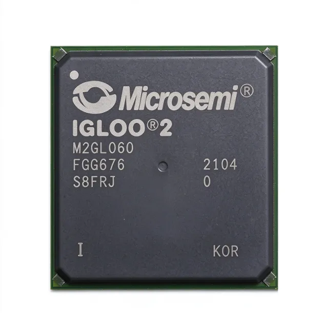
M2GL050-1FG896
M2GL050-1FG896 - 56K LLE IGLOO2 FPGA | Microchip
The Microchip Technology M2GL050-1FG896 is an IGLOO 2 flash FPGA with 56,340 logic elements, 377 user I/O, and 1.2 V core operation in an 896-pin FBGA package. The M2GL050-1FG896 combines programmable logic, embedded flash configuration memory, and a large ball-grid-array footprint in a single low-density device intended for bridging, I/O expansion, protocol conversion, system management, secure connectivity, image processing, and communications control functions.
An FPGA is a programmable semiconductor in the broader logic IC and semiconductor hierarchy. Unlike a fixed-function microcontroller or application-specific integrated circuit, an FPGA can be configured after manufacture to implement digital logic, state machines, interfaces, and parallel processing functions. The IGLOO 2 family combines reconfigurable logic with embedded flash, allowing the configuration to be retained in the device and supporting designs that need hardware flexibility without external configuration storage.
The M2GL050 family provides 56,340 logic elements and a 1.2 V core supply according to the manufacturer product information. Its 896-pin FBGA package exposes 377 I/O, creating a high pin-count interface for parallel buses, high-speed links, memory interfaces, control signals, and external converters. The package also makes component placement and escape routing a significant PCB-layout consideration compared with lower-pin-count devices.
The IGLOO 2 architecture supports general-purpose logic functions rather than hard processor cores. This makes it suitable for custom protocol bridges, data acquisition front ends, image and video processing pipelines, communications infrastructure, industrial controllers, and embedded security functions. Microchip identifies communications, industrial, medical, defense, and aviation markets as application areas for IGLOO 2 devices, while also noting uses that include Gigabit Ethernet control planes, dual PCI Express control planes, I/O expansion and conversion, and secure connectivity.
Because the M2GL050-1FG896 is configured through embedded flash, a complete design also requires a compatible bitstream, programming tool, pin-placement plan, and clocking strategy. Designers should preserve the manufacturer's recommended power, decoupling, and ball-grid-array layout rules. A fineless 896-pin FBGA also requires careful inspection, solder-paste control, and assembly-process qualification because solder-joint defects can create intermittent failures that are difficult to diagnose after deployment.
This product page combines the manufacturer family information with package, logic-cell, I/O, voltage, and lifecycle details. It also organizes replacement guidance, application fit, and design cautions so engineers can evaluate the M2GL050-1FG896 before committing a high-pin-count BGA layout to a new PCB.
The Microchip Technology M2GL050-1FG896 is an IGLOO 2 flash FPGA with 56,340 logic elements, 377 user I/O, and 1.2 V core operation in an 896-pin FBGA package. The M2GL050-1FG896 combines programmable logic, embedded flash configuration memory, and a large ball-grid-array footprint in a single low-density device intended for bridging, I/O expansion, protocol conversion, system management, secure connectivity, image processing, and communications control functions.
An FPGA is a programmable semiconductor in the broader logic IC and semiconductor hierarchy. Unlike a fixed-function microcontroller or application-specific integrated circuit, an FPGA can be configured after manufacture to implement digital logic, state machines, interfaces, and parallel processing functions. The IGLOO 2 family combines reconfigurable logic with embedded flash, allowing the configuration to be retained in the device and supporting designs that need hardware flexibility without external configuration storage.
The M2GL050 family provides 56,340 logic elements and a 1.2 V core supply according to the manufacturer product information. Its 896-pin FBGA package exposes 377 I/O, creating a high pin-count interface for parallel buses, high-speed links, memory interfaces, control signals, and external converters. The package also makes component placement and escape routing a significant PCB-layout consideration compared with lower-pin-count devices.
The IGLOO 2 architecture supports general-purpose logic functions rather than hard processor cores. This makes it suitable for custom protocol bridges, data acquisition front ends, image and video processing pipelines, communications infrastructure, industrial controllers, and embedded security functions. Microchip identifies communications, industrial, medical, defense, and aviation markets as application areas for IGLOO 2 devices, while also noting uses that include Gigabit Ethernet control planes, dual PCI Express control planes, I/O expansion and conversion, and secure connectivity.
Because the M2GL050-1FG896 is configured through embedded flash, a complete design also requires a compatible bitstream, programming tool, pin-placement plan, and clocking strategy. Designers should preserve the manufacturer's recommended power, decoupling, and ball-grid-array layout rules. A fineless 896-pin FBGA also requires careful inspection, solder-paste control, and assembly-process qualification because solder-joint defects can create intermittent failures that are difficult to diagnose after deployment.
This product page combines the manufacturer family information with package, logic-cell, I/O, voltage, and lifecycle details. It also organizes replacement guidance, application fit, and design cautions so engineers can evaluate the M2GL050-1FG896 before committing a high-pin-count BGA layout to a new PCB.
询价
联系我们