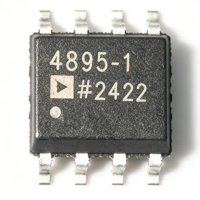
ADA4622-1ARJZ-R2
ADA4622-1ARJZ-R2 - 30V JFET Precision Op-Amp SOT-23-5 | ADI
The Analog Devices ADA4622-1ARJZ-R2 is a single-channel, 30 V, 8 MHz, low-bias-current, single-supply, rail-to-rail output (RRO) precision JFET operational amplifier in a 5-pin SOT-23 package supplied on a 7-inch reel of 250 units. It is the next-generation replacement for the legacy AD820/AD822 family, integrating JFET input stages with a precision bipolar output stage to deliver picoampere-level input bias current, low offset voltage, and rail-to-rail output swing while operating from a single 5 V to 30 V supply or dual ±5 V / ±15 V rails. According to the Analog Devices ADA4622-1/ADA4622-2/ADA4622-4 datasheet, the part is specified over the extended industrial temperature range of -40°C to +125°C and offers 8 MHz gain-bandwidth product with a typical slew rate that supports both DC precision and moderate-speed signal conditioning.
A precision operational amplifier is a high-gain DC-coupled analog building block used to amplify small differential signals while rejecting common-mode noise and offset drift. JFET-input op-amps (JFET op-amp = junction field-effect transistor op-amp) extend the input impedance into the gigaohm-to-teraohm range and reduce input bias current into the picoampere range, which is essential when interfacing with high-impedance sensors, photodiodes, and transimpedance topologies. The ADA4622-1 belongs to the operational amplifier -> amplifier IC -> analog IC -> integrated circuit hierarchy, and is targeted at applications where AD820/AD822 footprints, low IB, and rail-to-rail output are simultaneously required.
Key features include 8 MHz gain-bandwidth product, rail-to-rail output swing, picoampere-level input bias current, low input offset voltage, single-supply operation from 5 V to 30 V (and dual ±5 V / ±15 V), and an extended -40°C to +125°C industrial temperature range. The 5-lead SOT-23 (RJ) package is footprint-compatible with industry-standard single op-amp pinouts, easing migration from older AD820/AD822 designs. The part is specified at +5 V, ±5 V, and ±15 V supply rails, allowing a single BOM line to cover multiple system voltages.
Architecturally, the ADA4622-1 combines a JFET input differential pair with a precision output stage, allowing the high-impedance input behavior of JFETs without sacrificing the output drive strength needed for rail-to-rail swing into low-impedance loads. Designers should still observe standard precision-op-amp layout practices: low-leakage PCB guard rings around high-impedance nodes, minimal stray capacitance on the inverting input, and a stable feedback network chosen to account for the 8 MHz GBW.
Typical applications include photodiode transimpedance amplifiers (TIAs), precision instrumentation front-ends, high-impedance sensor signal conditioning, active filters, analog input stages for data acquisition boards, and pin-compatible upgrades of legacy AD820/AD822 designs. The combination of low IB, RRO, and wide supply range makes the part suitable for both single-supply battery-powered instrumentation and dual-supply industrial signal chains.
When designing with this device, keep high-impedance traces short and consider a PTFE or low-absorption PCB material if leakage budget is critical. Input bias-current cancellation is not required for most uses, but board cleanliness (no flux residue, no moisture) is essential to preserve picoampere-level IB performance.
This page synthesizes distributor pricing, verified cross-reference data from Analog Devices' SOT-23-5 footprint family, and practical PCB/layout guidance that complements (but does not duplicate) the manufacturer datasheet.
询价
联系我们