产品(32839)

ADA4896-2ARMZ - 1nV/√Hz Low Noise Dual Op Amp | Analog Devices
ADA4896-2ARMZ

ADA4896-2ARMZ - 1nV/√Hz Low Noise Dual Op Amp | Analog Devices

The ADA4896-2ARMZ is a dual, high-speed, voltage feedback operational amplifier from Analog Devices, offering an exceptional combination of low noise, low power, and rail-to-rail output. Housed in a compact 8-lead MSOP package, this amplifier is unity-gain stable and operates from a single 3V to 10V supply or dual ±1.5V to ±5V supplies. With a quiescent current of only 3 mA per amplifier, it delivers a bandwidth of 230 MHz and a slew rate of 120 V/µs, making it ideal for power-sensitive, high-performance signal conditioning. An operational amplifier (op amp) is a high-gain voltage amplifier with differential inputs and a single-ended output, used to perform mathematical operations like amplification, filtering, and signal conditioning. The ADA4896-2 is a voltage feedback op amp, a type that offers high input impedance and ease of use in inverting and non-inverting configurations. It belongs to the family of high-speed amplifiers, which are optimized for wide bandwidth and fast settling, essential in applications like ADC drivers, video processing, and active filters. As a rail-to-rail output amplifier, it can swing its output close to the supply rails, maximizing dynamic range in low-voltage systems. Key features of the ADA4896-2ARMZ include an ultra-low voltage noise density of 1 nV/√Hz at 100 kHz and 2.4 nV/√Hz at 10 Hz (1/f noise), a spurious-free dynamic range (SFDR) of -80 dBc at 2 MHz, and a low input bias current of 1.5 µA. The amplifier also provides a high open-loop gain of 100 dB and a common-mode rejection ratio (CMRR) of 100 dB, ensuring accurate signal processing. Its rail-to-rail output stage can drive loads as low as 50 Ω, and it is fully specified over the industrial temperature range of -40°C to +125°C. Technically, the ADA4896-2 uses a complementary bipolar process that achieves low noise without compromising speed or power. The amplifier's architecture includes a precision input stage that minimizes offset voltage (typically 0.5 mV) and drift, while the output stage provides high current drive capability. The device is designed for stable operation with capacitive loads up to 100 pF, and its internal compensation ensures unity-gain stability. The MSOP-8 package offers excellent thermal performance with a junction-to-ambient thermal resistance of 190°C/W, allowing operation in space-constrained designs. Typical applications include low-noise ADC drivers, high-speed active filters, photodiode amplification, and medical instrumentation. In ADC driver circuits, the ADA4896-2's low noise and high SFDR preserve signal integrity, while its rail-to-rail output maximizes the ADC's input range. For photodiode transimpedance amplifiers, the low input bias current and low noise enable precise detection of weak optical signals. In medical devices like ECG and EEG monitors, the amplifier's low noise and low power consumption are critical for battery-operated, high-resolution signal acquisition. When designing with the ADA4896-2ARMZ, ensure proper power supply decoupling with 0.1 µF ceramic capacitors placed close to the supply pins. The input common-mode voltage range extends to the negative rail, but for best performance, keep inputs within the specified range. The output can swing to within 50 mV of the rails, but for driving heavy loads, consider the output current capability. For optimal noise performance, use low-value resistors in the feedback network, as resistor noise can dominate.

询价 联系我们
ADA4896-2ARMZ-RL7 - Dual Low Noise RRO Op Amp | Analog Devices
ADA4896-2ARMZ-RL7

ADA4896-2ARMZ-RL7 - Dual Low Noise RRO Op Amp | Analog Devices

The ADA4896-2ARMZ-RL7 is a dual, unity-gain stable, low noise, rail-to-rail output, high speed voltage feedback amplifier from Analog Devices. It operates on a supply voltage range of 3 V to 10 V (or ±1.5 V to ±5 V) and features a quiescent current of 3 mA per amplifier. The device is available in an 8-lead MSOP package, making it suitable for space-constrained applications. What is a voltage feedback amplifier? A voltage feedback amplifier is a type of operational amplifier where the output voltage is fed back to the inverting input through a feedback network. It is characterized by its high input impedance, low output impedance, and high open-loop gain. Voltage feedback amplifiers are widely used in signal conditioning, filtering, and buffering applications due to their ease of use and stability. They form a subset of operational amplifiers, which are fundamental building blocks in analog signal processing. Key features of the ADA4896-2 include a low 1/f noise of 2.4 nV/√Hz at 10 Hz, a spurious-free dynamic range (SFDR) of -80 dBc at 2 MHz, and a unity-gain bandwidth of 230 MHz. The rail-to-rail output stage allows maximum output swing, and the low quiescent current makes it ideal for battery-powered systems. The amplifier also features a wide supply voltage range and is specified for operation over the industrial temperature range of -40°C to +125°C. The ADA4896-2 uses a complementary bipolar process technology, providing excellent DC precision and AC performance. The device is designed to drive high-speed ADCs and other capacitive loads, with a slew rate of 120 V/µs. Its low distortion and low noise make it suitable for high-performance signal chains. Typical applications include ADC drivers, active filters, instrumentation, and portable audio equipment. The low noise and high bandwidth make it ideal for medical imaging, communications, and test and measurement systems. When designing with the ADA4896-2, ensure proper power supply decoupling with 0.1 µF capacitors close to the supply pins. The rail-to-rail output stage requires careful consideration of the load impedance to maintain stability.

询价 联系我们
ADA4897-1ARZ - 1nV/√Hz Low Noise Op Amp | Analog Devices
ADA4897-1ARZ

ADA4897-1ARZ - 1nV/√Hz Low Noise Op Amp | Analog Devices

The ADA4897-1ARZ from Analog Devices is a unity-gain stable, low noise, rail-to-rail output, high speed voltage feedback amplifier in an 8-lead SOIC package. It operates from a 3V to 10V supply and delivers a 230 MHz bandwidth with a 120 V/µs slew rate. The device features an ultra-low wideband voltage noise of 1 nV/√Hz and a low 1/f noise of 2.4 nV/√Hz at 10 Hz, making it ideal for high-performance signal conditioning. An operational amplifier (op amp) is a high-gain voltage amplifier with differential inputs and a single-ended output. It is a fundamental building block in analog electronics, used in applications ranging from signal conditioning to active filtering. The ADA4897-1 is a voltage feedback amplifier, a type of op amp that uses a voltage-controlled voltage source topology, offering high bandwidth and low distortion. It belongs to the family of high-speed amplifiers, which are optimized for fast settling and wide bandwidth, and is part of the broader category of linear integrated circuits. Key features include a low input offset voltage of 0.5 mV (typical), a quiescent current of only 3 mA per amplifier, and a spurious-free dynamic range (SFDR) of -80 dBc at 2 MHz. The rail-to-rail output stage allows maximum output swing, and the device is unity-gain stable, simplifying design in buffer and follower configurations. The ADA4897-1 also offers low distortion of -115 dBc at 100 kHz with a 2 V p-p output, ensuring high signal fidelity. Technically, the ADA4897-1 uses a complementary bipolar process that achieves its low noise and high speed. The amplifier's input stage is optimized for low voltage noise, while the output stage provides rail-to-rail swing with low output impedance. The device is specified over the industrial temperature range of -40°C to +125°C, and it is available in an 8-lead SOIC package (ARZ suffix), which is suitable for space-constrained designs. Typical applications include low noise instrumentation, active filters, ADC drivers, and high-speed signal conditioning in test and measurement equipment. The low noise and high bandwidth make it particularly suited for medical imaging, communications, and industrial process control. In these applications, the ADA4897-1 ensures accurate signal reproduction with minimal added noise. When designing with the ADA4897-1, pay attention to power supply decoupling: place a 0.1 µF ceramic capacitor close to each supply pin and a 10 µF tantalum capacitor at the supply rails. Also, consider the thermal performance, as the SOIC package has a limited power dissipation capability; ensure the junction temperature stays below 150°C.

询价 联系我们
ADA4897-1ARZ-RL7 - 1nV/√Hz Low Noise Op Amp | Analog Devices
ADA4897-1ARZ-RL7

ADA4897-1ARZ-RL7 - 1nV/√Hz Low Noise Op Amp | Analog Devices

The ADA4897-1ARZ-RL7 is a unity-gain stable, low noise, rail-to-rail output, high speed voltage feedback amplifier from Analog Devices. It operates from a 3V to 10V supply and delivers a gain bandwidth product of 230 MHz with a slew rate of 120 V/µs. The device is available in an 8-pin SOIC package and is designed for applications requiring low noise and low power consumption. An operational amplifier (op amp) is a high-gain voltage amplifier with differential inputs and a single-ended output. It is a fundamental building block in analog electronics, used in signal conditioning, filtering, and amplification. The ADA4897-1 is a voltage feedback amplifier, which offers high bandwidth and low distortion, making it suitable for high-speed signal processing. Key features include ultra-low wideband noise of 1 nV/√Hz, low 1/f noise of 2.4 nV/√Hz at 10 Hz, and low distortion of -115 dBc at 100 kHz. The quiescent current is only 3 mA per amplifier, making it power-efficient. The rail-to-rail output stage allows maximum output swing, and the device is unity-gain stable, simplifying design. The ADA4897-1 uses a complementary bipolar process, achieving excellent noise performance and high speed. The input offset voltage is low, and the device has a high open-loop gain, ensuring accurate signal amplification. The amplifier is designed to drive capacitive loads and provides a spurious-free dynamic range of -80 dBc at 2 MHz. Typical applications include ultrasound, low noise PLLs, and high-speed instrumentation. The low noise and high bandwidth make it ideal for medical imaging, communications, and test equipment. The rail-to-rail output is beneficial in single-supply systems, and the low power consumption extends battery life in portable devices. When designing with this amplifier, ensure proper power supply decoupling with 0.1 µF capacitors close to the supply pins. The input common-mode range extends to the negative rail, but for best performance, keep inputs within the specified range. The output can swing close to the rails, but avoid heavy loads that may reduce output swing.

询价 联系我们
ADA4897-2ARMZ - Dual Low Noise RRO Op Amp | Analog Devices
ADA4897-2ARMZ

ADA4897-2ARMZ - Dual Low Noise RRO Op Amp | Analog Devices

The ADA4897-2ARMZ is a dual, unity-gain stable, low noise, rail-to-rail output, high speed voltage feedback amplifier from Analog Devices. It operates from a 3 V to 10 V supply and features a quiescent current of 3 mA per amplifier. The device is available in a 10-lead MSOP package, making it suitable for space-constrained applications. An operational amplifier (op amp) is a high-gain voltage amplifier with differential inputs and a single-ended output. It is a fundamental building block in analog signal processing, used in applications ranging from signal conditioning to active filtering. The ADA4897-2 belongs to the class of high-speed, low-noise amplifiers, which are essential in precision instrumentation and communication systems where signal integrity is critical. Key features of the ADA4897-2 include a low input voltage noise of 1 nV/√Hz, a 1/f noise corner of 2.4 nV/√Hz at 10 Hz, and a spurious-free dynamic range (SFDR) of 80 dBc at 2 MHz. The amplifier also provides a bandwidth of 230 MHz and a slew rate of 120 V/µs, enabling fast signal processing. The rail-to-rail output stage maximizes dynamic range, making it ideal for single-supply applications. The ADA4897-2 uses a voltage feedback architecture with complementary bipolar transistors, achieving low distortion and high linearity. The device is fully specified over the industrial temperature range of -40°C to +125°C. Its low power consumption and high speed make it a versatile choice for battery-powered and high-density systems. Typical applications include ultrasound equipment, low noise PLL filters, high performance ADC drivers, and high speed signal conditioning. The amplifier's low noise and high bandwidth ensure accurate signal reproduction in these demanding environments. When designing with the ADA4897-2, proper power supply decoupling is essential to maintain stability and minimize noise. Use 0.1 µF ceramic capacitors close to the supply pins and a 10 µF tantalum capacitor for bulk decoupling. The output can drive capacitive loads up to 100 pF without oscillation, but for larger loads, an isolation resistor may be required.

询价 联系我们
ADA4897-2ARMZ-RL7 - Dual 1nV/√Hz Low Noise Op Amp | Analog Devices
ADA4897-2ARMZ-RL7

ADA4897-2ARMZ-RL7 - Dual 1nV/√Hz Low Noise Op Amp | Analog Devices

The ADA4897-2ARMZ-RL7 is a dual, unity-gain stable, low noise, rail-to-rail output, high speed voltage feedback amplifier from Analog Devices. It operates over a supply range of 3 V to 10 V and features a quiescent current of 3 mA per amplifier. The device is offered in a 10-lead MSOP package, making it suitable for space-constrained applications. An operational amplifier (op amp) is a high-gain voltage amplifier with differential inputs and a single-ended output. It is a fundamental building block in analog signal processing, used in applications such as filtering, amplification, and signal conditioning. The ADA4897-2 belongs to the class of high-speed, low-noise op amps, which are essential in precision instrumentation and communication systems. Key features include a voltage noise density of 1 nV/√Hz at 100 kHz, 1/f noise of 2.4 nV/√Hz at 10 Hz, and a spurious-free dynamic range (SFDR) of -80 dBc at 2 MHz. The amplifier provides a slew rate of 120 V/µs and a gain-bandwidth product of 230 MHz. It also features rail-to-rail output swing, enabling maximum dynamic range in low-voltage applications. The ADA4897-2 uses a complementary bipolar process, achieving low distortion and high linearity. The device is fully specified over the extended industrial temperature range of -40°C to +125°C. Its low noise and high speed make it ideal for driving high-resolution ADCs, ultrasound front-ends, and low-noise signal chains. Typical applications include ultrasound imaging, low-noise PLL loop filters, high-speed ADC drivers, and active filters. The dual configuration allows compact designs for stereo audio or multi-channel data acquisition. The rail-to-rail output ensures efficient use of the supply voltage, which is critical in battery-powered systems. When designing with this amplifier, ensure proper power supply decoupling with 0.1 µF ceramic capacitors close to the supply pins. The thermal pad (if present) should be connected to a low-impedance ground plane for optimal thermal performance. The input common-mode range extends to the negative rail, but not to the positive rail, so level shifting may be required for single-supply applications.

询价 联系我们
ADA4940-1ACPZ - Ultralow Power Differential ADC Driver | Analog Devices
ADA4940-1ACPZ

ADA4940-1ACPZ - Ultralow Power Differential ADC Driver | Analog Devices

The ADA4940-1ACPZ from Analog Devices is a high speed, low power differential amplifier designed to drive high performance analog-to-digital converters (ADCs). It operates from a single 3.3V to 5V supply or dual supplies, consuming only 1.25 mA quiescent current, making it ideal for battery-powered and portable applications. The device provides two closely balanced differential outputs from either differential or single-ended inputs, with a common-mode output voltage that is adjustable to match the ADC input range. A differential amplifier is an electronic amplifier that amplifies the difference between two input voltages while rejecting common-mode signals. In the context of ADC driving, it converts a single-ended signal into a balanced differential signal, improving noise immunity and increasing the dynamic range of the data acquisition system. The ADA4940-1 is fabricated on Analog Devices' advanced dielectrically isolated SiGe bipolar process, enabling high speed and low distortion. Key features include ultralow power consumption of 1.25 mA, low noise and low distortion, and a bandwidth of 34 MHz. The device supports resolutions up to 18 bits from DC to 1 MHz, making it suitable for precision data acquisition. The output common-mode voltage is adjustable via a dedicated pin, allowing direct interface to SAR and sigma-delta ADCs. The ADA4940-1 is available in a Pb-free, 3 mm × 3 mm, 16-lead LFCSP package, which is compact and suitable for space-constrained designs. Technical depth: The ADA4940-1 uses a differential architecture with internal feedback, providing excellent gain accuracy and low offset. The device features a disable pin that reduces supply current to 10 µA, enabling power cycling in portable systems. The input voltage noise is 3.9 nV/√Hz, and the distortion at 1 MHz is -100 dBc, ensuring high signal fidelity. The device operates over the industrial temperature range of -40°C to +125°C. Typical applications include driving SAR and sigma-delta ADCs in medical instrumentation, industrial process control, and portable data acquisition systems. The low power and small package make it ideal for battery-powered devices such as portable medical monitors and handheld test equipment. Design consideration: To achieve optimal performance, place a 0.1 µF decoupling capacitor close to each supply pin and use a ground plane to minimize noise. The output common-mode voltage should be set to the ADC's reference midpoint for best dynamic range.

询价 联系我们
ADA4940-1ACPZ-RL7 - Ultralow Power Differential ADC Driver | ADI
ADA4940-1ACPZ-RL7

ADA4940-1ACPZ-RL7 - Ultralow Power Differential ADC Driver | ADI

The ADA4940-1ACPZ-RL7 from Analog Devices is a low noise, low distortion fully differential amplifier designed to drive high-performance SAR and sigma-delta analog-to-digital converters (ADCs) with resolutions up to 18 bits. Operating on a mere 1.25 mA of quiescent current, it is an ideal choice for power-sensitive applications. The device is available in a compact 16-lead LFCSP-VQ (3x3 mm) package, making it suitable for space-constrained designs. A fully differential amplifier (FDA) is an amplifier that converts a single-ended input signal into a differential output, or amplifies a differential input while rejecting common-mode noise. It is a critical building block in precision data acquisition systems, providing the balanced drive required by high-resolution ADCs. The ADA4940-1 belongs to the family of differential amplifiers, which are a subset of operational amplifiers used specifically for driving ADCs and transmitting signals over long lines. Key features include ultralow power consumption of 1.25 mA quiescent current, low noise and distortion, and an adjustable output common-mode voltage. The device supports a wide supply range and provides excellent AC performance, making it suitable for applications from DC to 1 MHz. The ADA4940-1 is optimized for driving the PULSAR family of ADCs from Analog Devices, ensuring seamless integration. Technically, the ADA4940-1 employs a precision architecture that maintains low offset and high linearity. The adjustable common-mode output allows direct interface to ADC inputs, eliminating the need for external level shifting. The device also features a power-down mode to conserve energy in battery-powered systems. Its low power consumption does not compromise performance, making it a standout choice for portable instrumentation. Typical applications include driving SAR ADCs in medical imaging, industrial process control, and portable battery-powered devices. The ADA4940-1 is also used in communication systems where signal integrity is paramount. Its low power and small footprint make it ideal for multi-channel data acquisition systems. When designing with this device, ensure proper decoupling of the power supply pins and careful layout of the differential traces to minimize parasitic capacitance. The output common-mode voltage should be set to match the ADC's input range for optimal performance.

询价 联系我们
ADA4940-2ACPZ - Low Power Differential ADC Driver | Analog Devices
ADA4940-2ACPZ

ADA4940-2ACPZ - Low Power Differential ADC Driver | Analog Devices

The Analog Devices ADA4940-2ACPZ is a dual, low power, fully differential amplifier designed for driving high-resolution SAR and sigma-delta ADCs. It operates from a single 3.3V to 7V supply or dual supplies up to ±3.5V, consuming only 1.25 mA quiescent current per amplifier. The device provides two closely balanced differential outputs from either differential or single-ended inputs, making it ideal for precision data acquisition systems. A fully differential amplifier (FDA) is an amplifier with differential inputs and differential outputs, used to convert single-ended signals to differential, buffer differential signals, and drive ADCs. It is a key building block in signal chains, sitting between the sensor/amplifier stage and the ADC, ensuring optimal signal integrity and common-mode rejection. The ADA4940-2 belongs to the family of differential amplifiers, which are a subset of operational amplifiers, which are part of the broader category of analog integrated circuits. Key features include a -3 dB bandwidth of 26 MHz, a slew rate of 45 V/µs, and a low input voltage noise of 3.9 nV/√Hz. The device achieves a spurious-free dynamic range (SFDR) of -110 dBc at 100 kHz and a THD of -110 dB at 100 kHz, ensuring high fidelity for precision applications. It also features an output common-mode voltage control pin (VOCM) for level shifting, and a power-down pin for standby operation. The ADA4940-2 is fabricated on Analog Devices' advanced dielectrically isolated SiGe bipolar process, providing excellent DC accuracy with a maximum input offset voltage of 150 µV and a typical offset drift of 0.5 µV/°C. The device is available in a Pb-free, 4 mm × 4 mm, 24-lead LFCSP package, which is compact and suitable for space-constrained designs. Typical applications include driving PULSAR ADCs, such as the AD7985 and AD7986, in medical imaging, industrial process control, and instrumentation. The low power consumption and high performance make it suitable for battery-powered portable devices and multi-channel data acquisition systems. When designing with the ADA4940-2, ensure proper supply decoupling with 0.1 µF capacitors close to the supply pins. The VOCM pin should be driven by a low-impedance source to set the output common-mode voltage, and the feedback network should be matched to maintain balance and minimize distortion.

询价 联系我们
ADA4940-2ACPZ-RL7 - Ultralow Power ADC Driver | Analog Devices
ADA4940-2ACPZ-RL7

ADA4940-2ACPZ-RL7 - Ultralow Power ADC Driver | Analog Devices

The ADA4940-2ACPZ-RL7 from Analog Devices is a dual, ultralow power, low distortion fully differential amplifier (FDA) designed to drive high-performance SAR and sigma-delta ADCs with resolutions up to 18 bits. Operating from a single 3.3V to 7V supply or dual supplies up to ±3.5V, it consumes only 1.25 mA of quiescent current per amplifier, making it ideal for battery-powered and power-sensitive applications. The device is housed in a 24-lead LFCSP (4mm x 4mm) package with an exposed pad for enhanced thermal performance. A fully differential amplifier (FDA) is an operational amplifier with differential inputs and differential outputs, providing balanced signals that reject common-mode noise and even-order harmonics. FDAs are essential in precision data acquisition systems, where they convert single-ended signals to differential for driving ADCs, improving dynamic range and reducing distortion. The ADA4940-2 belongs to the ADA4940 family, which includes the single-channel ADA4940-1 and the dual ADA4940-2, both offering the same low noise and low distortion performance. Key features include a low input voltage noise of 3.9 nV/√Hz, a spurious-free dynamic range (SFDR) of -110 dBc at 100 kHz, and a -3 dB bandwidth of 26 MHz. The output common-mode voltage is adjustable via a VOCM pin, allowing precise level shifting to match the ADC input range. The device also features a disable pin for power-down, reducing quiescent current to 10 µA, and an internal common-mode feedback loop that maintains output balance. The ADA4940-2 uses a precision bipolar process with laser-trimmed thin-film resistors, achieving low DC offset (typically 50 µV) and excellent gain accuracy. Its differential output swing is rail-to-rail, and it can drive capacitive loads up to 10 pF without oscillation. The device is fully specified over the -40°C to +125°C temperature range, ensuring reliable operation in industrial and automotive environments. Typical applications include driving SAR ADCs such as the AD7985 and AD7768, medical imaging systems, portable instrumentation, and communications receivers. The low power consumption and small footprint make it suitable for multi-channel data acquisition systems where board space and thermal budget are constrained. When designing with the ADA4940-2, ensure proper supply decoupling with 0.1 µF and 10 µF capacitors close to the VCC and VEE pins. The VOCM pin should be driven by a low-impedance source to avoid common-mode errors. For optimal distortion, keep the feedback resistor values between 200 Ω and 1 kΩ and minimize parasitic capacitance at the summing nodes.

询价 联系我们
ADA4941-1ARZ - 18-Bit Differential ADC Driver | Analog Devices
ADA4941-1ARZ

ADA4941-1ARZ - 18-Bit Differential ADC Driver | Analog Devices

The ADA4941-1ARZ is a low power, single-ended input, differential output amplifier optimized for driving high resolution analog-to-digital converters (ADCs). Manufactured on Analog Devices' proprietary second-generation eXtra fast complementary bipolar (XFCB) process, it achieves 18-bit performance on low supply currents. The device is configured in an easy-to-use, single-ended-to-differential gain of +2 configuration, making it ideal for precision data acquisition systems. A differential ADC driver is an amplifier that converts a single-ended input signal into a differential output, which is required by many high-performance ADCs to improve noise immunity and dynamic range. The ADA4941-1 belongs to the class of differential amplifiers, which are essential building blocks in signal chains for precision measurement, medical imaging, and communications. By providing a balanced output, it enables the full-scale input range of the ADC to be utilized, enhancing the signal-to-noise ratio (SNR) and reducing even-order harmonics. Key features include ultralow distortion of 120 dBc THD at 10 kHz, low noise achieving 97 dB SNR at 100 kHz with 4 V p-p output, and extremely low power consumption on a 3 V supply. The device operates from a single supply, simplifying power design. It offers high input impedance, which minimizes loading on the preceding stage. The ADA4941-1 is available in an 8-lead SOIC package (ARZ suffix), suitable for space-constrained applications. Technically, the ADA4941-1 uses a differential architecture with an internal common-mode feedback loop that sets the output common-mode voltage to a reference level, typically mid-supply. This allows direct coupling to ADCs with a specified common-mode input range. The XFCB process provides high-speed complementary bipolar transistors with excellent matching, contributing to the low distortion and noise performance. The device is stable with capacitive loads, simplifying PCB layout. Typical applications include driving 16-bit and 18-bit PulSAR ADCs such as the AD7687, AD7690, and AD7691. It is also used in industrial process control, medical instrumentation, and communications systems where high resolution and low power are critical. The single-ended-to-differential conversion capability makes it versatile for interfacing sensors and transducers to differential ADCs. When designing with the ADA4941-1, ensure proper supply decoupling with 0.1 uF and 10 uF capacitors close to the VCC and VEE pins. The output common-mode voltage can be adjusted via the VOCM pin to match the ADC input range. For optimal performance, use precision resistors with low temperature coefficient for the gain-setting network.

询价 联系我们
ADA4941-1ARZ-RL7 - Differential ADC Driver | Analog Devices
ADA4941-1ARZ-RL7

ADA4941-1ARZ-RL7 - Differential ADC Driver | Analog Devices

The ADA4941-1ARZ-RL7 is a low power, single-ended input, differential output amplifier optimized for driving high resolution analog-to-digital converters (ADCs). Manufactured by Analog Devices on their proprietary second-generation eXtra fast complementary bipolar (XFCB) process, this device achieves 18-bit performance on low supply currents. It is configured in an easy-to-use, single-ended-to-differential gain of +2 configuration, making it ideal for driving 16-bit and 18-bit PulSAR ADCs such as the AD7687, AD7690, and AD7691. A differential ADC driver is an amplifier that converts a single-ended input signal into a differential output, which is required by many high-performance ADCs to improve noise immunity and dynamic range. The ADA4941-1 belongs to the category of differential amplifiers, which are a subset of operational amplifiers used in signal conditioning chains. These amplifiers are essential in precision data acquisition systems where the ADC's performance depends on the quality of the driving signal. Key features of the ADA4941-1 include ultralow distortion of 120 dBc THD at 10 kHz, low noise enabling 97 dB SNR at 100 kHz with a 4 V p-p output, and extremely low power consumption on a 3 V supply. The device operates from a single supply, simplifying power supply design. Its high input impedance minimizes loading on the source, and the differential output provides the balanced drive required by modern ADCs. Technically, the ADA4941-1 uses a single-ended to differential conversion with a fixed gain of +2, eliminating the need for external gain-setting resistors. The output common-mode voltage is set by an internal reference, ensuring proper ADC input range. The XFCB process provides high speed and low distortion while maintaining low power, making it suitable for battery-powered and portable instrumentation. Typical applications include driving 16-bit and 18-bit SAR ADCs in medical imaging, industrial process control, and precision data acquisition systems. The device is also used in communication systems where high dynamic range is required. Its low power consumption makes it ideal for portable and battery-operated equipment. When designing with the ADA4941-1, ensure that the input signal is within the common-mode input range and that the output is properly filtered to avoid aliasing. The device is available in an 8-lead SOIC package, and the RL7 suffix indicates tape and reel packaging for automated assembly.

询价 联系我们
ADA4945-1ACPZ - Low-Noise FDA ADC Driver, 3-10V | Analog Devices
ADA4945-1ACPZ

ADA4945-1ACPZ - Low-Noise FDA ADC Driver, 3-10V | Analog Devices

The Analog Devices ADA4945-1ACPZ is a low-noise, low-distortion, fully differential amplifier (FDA) with two selectable power modes, designed to drive high-performance ADCs in data acquisition and signal processing systems. It operates from a 3 V to 10 V supply, delivers rail-to-rail differential outputs, and is housed in a 16-lead LFCSP (3 mm × 3 mm) package. The two power modes (full power and low power) let designers trade quiescent current against bandwidth and input voltage noise (1.8 nV/√Hz typical in full power mode). A fully differential amplifier (FDA) is an op-amp derivative with differential inputs and differential outputs. FDAs sit in the signal-chain hierarchy between operational amplifiers and differential amplifiers, providing common-mode rejection, suppressing even-order harmonics, and converting single-ended signals into balanced differential signals for modern differential-input ADCs. The ADA4945-1 belongs to the broader analog IC category, specifically under amplifier ICs and the special-purpose ADC-driver sub-family. Key specifications include 0.1 µV/°C offset drift, low DC offset, an output common-mode (VOCM) pin for setting the ADC input common-mode voltage, adjustable output common-mode, output limiting for ADC overdrive protection, and excellent dynamic performance. The high-voltage SiGe complementary bipolar process enables operation up to 10 V — higher than many competing FDAs — providing headroom for ADCs with wider input ranges. Technically, the SiGe dielectrically-isolated process delivers low distortion and low input voltage noise simultaneously, while the selectable power-mode pin optimizes current draw for either maximum bandwidth or low-power applications. The differential output stage provides two closely balanced outputs in response to either differential or single-ended inputs, simplifying the interface to differential ADCs such as the AD9680, AD9268, and AD9656. Typical applications include high-speed ADC drivers, medical imaging front ends, communications receivers, IF and baseband signal chains, and industrial instrumentation. The low offset drift maintains DC accuracy over temperature, while rail-to-rail outputs maximize dynamic range in low-voltage systems. When designing with the ADA4945-1, set VOCM to match the ADC input common-mode voltage, select the appropriate power mode for the bandwidth/power trade-off, and follow the datasheet PCB layout guidelines to minimize parasitic capacitance and preserve signal integrity at high frequencies. This page synthesizes distributor pricing, drop-in pin-compatible alternatives, and practical design notes not found on the manufacturer datasheet alone.

询价 联系我们
ADA4945-1ACPZ-RL7 - Low Noise FDA ADC Driver | Analog Devices
ADA4945-1ACPZ-RL7

ADA4945-1ACPZ-RL7 - Low Noise FDA ADC Driver | Analog Devices

The ADA4945-1ACPZ-RL7 from Analog Devices is a low-noise, low-distortion, fully differential amplifier (FDA) designed for driving high-performance ADCs. It operates over a broad power supply range of 3 V to 10 V and features two selectable power modes, allowing designers to optimize between power consumption and dynamic performance. The device is offered in a compact 16-lead LFCSP (3x3 mm) package, making it suitable for space-constrained applications. A fully differential amplifier (FDA) is an amplifier with differential inputs and differential outputs, providing balanced signals that reject common-mode noise and even-order harmonics. FDAs are essential in high-speed signal chains, particularly for driving ADCs, where they convert single-ended signals to differential, provide gain, and buffer the ADC input. The ADA4945-1 fits into the hierarchy: fully differential amplifier -> differential amplifier -> operational amplifier -> analog IC -> semiconductor. Key features include ultra-low DC offset and offset drift (0.1 µV/°C), high speed, and excellent distortion performance. The device achieves low noise and low distortion, making it ideal for data acquisition systems requiring high accuracy. The two power modes allow a trade-off between power dissipation and bandwidth, enabling efficient operation in battery-powered or high-performance systems. Technically, the ADA4945-1 uses a precision architecture with internal common-mode feedback, ensuring accurate output common-mode voltage control. It provides a wide input common-mode range and rail-to-rail output, simplifying interface with various ADC inputs. The device also includes a disable feature for power saving, and its small package minimizes board space. Typical applications include driving high-speed ADCs in communications, instrumentation, and medical imaging systems. It is also used in single-ended to differential conversion, level shifting, and as a buffer for precision references. The low offset drift ensures stable performance over temperature, critical for precision measurement. When designing with the ADA4945-1, ensure proper power supply decoupling with 0.1 µF and 10 µF capacitors close to the pins. The feedback network must be carefully matched to maintain balance and minimize distortion. The device's power mode selection should be based on the required bandwidth and power budget.

询价 联系我们
ADA4950-1YCPZ - Differential ADC Driver G=1/2/3 | ADI
ADA4950-1YCPZ

ADA4950-1YCPZ - Differential ADC Driver G=1/2/3 | ADI

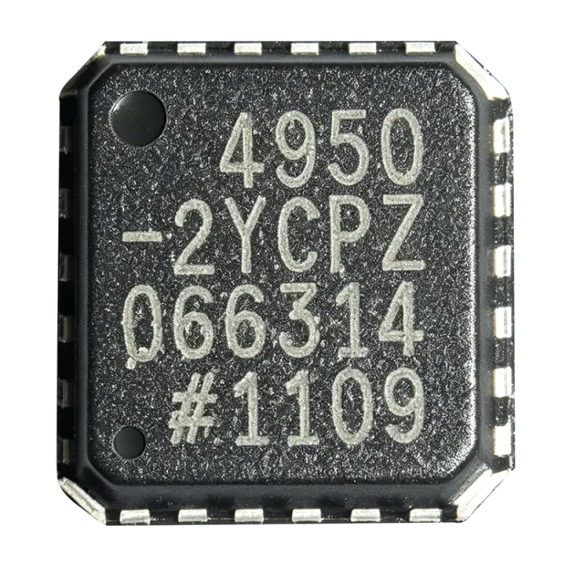
The ADA4950-1YCPZ is a low power, selectable gain differential ADC driver from Analog Devices, Inc. It provides fixed gains of 1, 2, or 3 using on-chip feedback and gain resistors, eliminating the need for external resistor networks and reducing BOM area. The device is packaged in a 16-lead LFCSP-VQ (3x3 mm) and supports a single supply range of 3 V to 11 V or a dual supply range of ±1.5 V to ±5.5 V. It is designed for driving high performance analog-to-digital converters (ADCs) in both single-ended-to-differential and differential-to-differential configurations. A differential ADC driver is a specialized amplifier that converts a single-ended or differential analog signal into a balanced differential output centered at a desired common-mode voltage, which is essential for driving modern high-speed ADCs. These converters rely on differential inputs to improve common-mode noise rejection, reduce even-order harmonic distortion, and double the dynamic range compared with single-ended driver solutions. Within the signal chain hierarchy, the ADC driver sits between the anti-aliasing filter and the converter input, providing scaling, buffering, and level shifting. Key features of the ADA4950-1 include on-chip gain select pins for G=1, 2, 3, low power consumption enabled by the proprietary silicon-germanium (SiGe) complementary bipolar process, and 114 mA output current per channel. The internal feedback network maintains excellent gain accuracy without external precision resistors, and the low distortion and noise floor suit demanding data acquisition and communications applications. The SiGe complementary bipolar fabrication process provides the ADA4950-1 with a favorable speed-to-power ratio, making it possible to achieve wide bandwidths and low harmonic distortion while consuming less quiescent current than amplifiers built in older bipolar processes. The ADA4950-1 is the single-channel version; the ADA4950-2 is the dual-channel companion for multichannel systems. Typical applications include high-speed ADC input stages in instrumentation, IF sampling and baseband signal chains in software-defined radios, differential buffering for sensors, and ultrasound and radar preprocessing. The 3x3 mm LFCSP package supports compact board layouts. When designing with the ADA4950-1, connect the gain select pins according to the desired closed-loop gain and place 0.1 uF decoupling capacitors as close as possible to the supply pins. The output common-mode voltage must be set within the ADC input range to avoid clipping and preserve converter dynamic performance.

询价 联系我们
ADA4950-1YCPZ-RL7 - Selectable Gain Diff ADC Driver | Analog Devices
ADA4950-1YCPZ-RL7

ADA4950-1YCPZ-RL7 - Selectable Gain Diff ADC Driver | Analog Devices

The ADA4950-1YCPZ-RL7 from Analog Devices is a low power, selectable gain differential ADC driver with on-chip feedback and gain resistors. It is a gain-selectable version of the ADA4932-1, offering gains of 1, 2, and 3 without external resistors. The device is housed in a 16-lead LFCSP-VQ (3x3 mm) package and is designed to drive high performance analog-to-digital converters (ADCs) in both single-ended-to-differential and differential-to-differential configurations. A differential amplifier is an electronic amplifier that amplifies the difference between two input voltages while rejecting common-mode signals. In the signal chain hierarchy, a differential ADC driver sits between the sensor or analog front-end and the ADC, converting single-ended signals to differential or buffering differential signals to provide the low impedance, high linearity drive required for high-resolution conversion. This function is critical in applications such as communications, instrumentation, and medical imaging where signal integrity directly impacts system performance. Key features of the ADA4950-1 include selectable gains of 1, 2, and 3 via a single gain pin, eliminating the need for external resistor networks and reducing component count. The device operates from a single 3.3V to 5V supply or dual supplies up to ±5V, and features a wide bandwidth suitable for driving ADCs with sample rates up to 100 MSPS. The low power consumption of 5.5 mA quiescent current makes it ideal for battery-powered and channel-dense systems. The output common-mode voltage is adjustable, allowing direct interface to ADC input ranges. Technically, the ADA4950-1 uses an internal feedback network with precision laser-trimmed resistors to achieve accurate gains and low distortion. The device provides a differential output with a common-mode reference pin (VOCM) that sets the output common-mode level, simplifying ADC interface design. The input voltage noise is 3.5 nV/√Hz, and the spurious-free dynamic range (SFDR) is excellent, ensuring high fidelity signal conversion. The LFCSP package with exposed pad offers good thermal performance and a compact footprint for space-constrained designs. Typical applications include driving high-speed ADCs in communications receivers, medical ultrasound equipment, and test and measurement instruments. The selectable gain feature allows the same board design to accommodate different input signal levels, reducing design time and BOM cost. The device is also suitable for differential signaling over twisted-pair cables in industrial and automotive systems. When designing with the ADA4950-1, ensure proper power supply decoupling with 0.1 µF and 10 µF capacitors close to the supply pins. The VOCM pin should be driven by a low-impedance source to set the output common-mode voltage accurately. The gain select pin (G1) must be tied to the appropriate logic level to achieve the desired gain, and the input pins should be AC-coupled if the source has a DC offset.

询价 联系我们
ADA4950-2YCPZ - Dual Differential ADC Driver | Analog Devices
ADA4950-2YCPZ

ADA4950-2YCPZ - Dual Differential ADC Driver | Analog Devices

The ADA4950-2YCPZ is a dual, gain-selectable differential amplifier from Analog Devices, designed as a high-performance ADC driver. It is a member of the ADA4950 family, which includes the ADA4950-1 (single) and ADA4950-2 (dual) versions. These amplifiers feature on-chip feedback and gain resistors, allowing fixed gains of 1, 2, and 3 without external components. The ADA4950-2 is fabricated using Analog Devices' proprietary silicon-germanium (SiGe) complementary bipolar process, which enables low distortion and low noise at low power consumption. The device operates from a single 3.3V to 11V supply or dual ±1.65V to ±5.5V supplies, and is available in a 24-lead LFCSP (4x4 mm) package. A differential amplifier is an electronic amplifier that amplifies the difference between two input voltages while rejecting common-mode signals. In the context of ADC driving, a differential amplifier converts a single-ended signal to a differential signal or buffers a differential signal, providing the necessary drive strength and level shifting to interface with high-performance analog-to-digital converters. The ADA4950-2 is specifically optimized for this role, offering low noise, low distortion, and high bandwidth to preserve signal integrity. Key features of the ADA4950-2 include a -3 dB bandwidth of 1.35 GHz (gain = 1), a slew rate of 2900 V/µs, and a low input voltage noise of 2.2 nV/√Hz. The device provides a differential output with a common-mode voltage set by an internal reference, simplifying interface to ADCs. It also features a power-down mode to conserve energy when not in use. The on-chip gain resistors eliminate the need for external resistor networks, reducing board space and component count. The ADA4950-2 is well-suited for a wide range of applications, including communications, instrumentation, and medical imaging. Its high bandwidth and low distortion make it ideal for driving high-speed ADCs in software-defined radios, radar systems, and test equipment. The low power consumption (typically 9.5 mA per amplifier) is beneficial for portable and battery-powered devices. When designing with the ADA4950-2, it is important to consider proper power supply decoupling and PCB layout to achieve optimal performance. The exposed pad on the LFCSP package should be soldered to a ground plane for thermal and electrical performance. Additionally, the input common-mode voltage range and output swing should be checked against the ADC's input requirements to ensure proper operation.

询价 联系我们
ADA4950-2YCPZ-RL7 - Selectable Gain Diff ADC Driver | Analog Devices
ADA4950-2YCPZ-RL7

ADA4950-2YCPZ-RL7 - Selectable Gain Diff ADC Driver | Analog Devices

The ADA4950-2YCPZ-RL7 is a dual, low power, selectable gain differential ADC driver from Analog Devices. It is a gain-selectable version of the ADA4932-2, featuring on-chip feedback and gain resistors that allow the user to select gains of 1, 2, or 3 without external components. This device is designed to drive high-performance analog-to-digital converters (ADCs) in both single-ended-to-differential and differential-to-differential configurations. Housed in a compact 24-lead LFCSP (4x4 mm) package, it operates from a single 3.3V to 11V supply or dual ±1.65V to ±5.5V supplies, making it versatile for various signal chain designs. A differential ADC driver is a specialized amplifier that converts a single-ended or differential input signal into a balanced differential output, optimized to interface with the differential inputs of high-speed ADCs. It provides the necessary gain, common-mode voltage shifting, and low output impedance to drive the ADC's sampling capacitor without degrading signal integrity. In the signal chain hierarchy, a differential ADC driver sits between the sensor/amplifier stage and the ADC, ensuring that the ADC receives a clean, well-conditioned signal for accurate conversion. Key features of the ADA4950-2 include a wide -3 dB bandwidth of 750 MHz, a slew rate of 2900 V/µs, and a low input voltage noise of 2.2 nV/√Hz. The device also offers a low offset voltage of 200 µV and a high output current of 60 mA, enabling it to drive the capacitive loads of ADCs effectively. The selectable gain feature simplifies design by eliminating the need for external resistor networks, reducing board space and component count. Fabricated using Analog Devices' proprietary silicon-germanium (SiGe) complementary bipolar process, the ADA4950-2 achieves low distortion and noise at low power consumption. The device features a power-down mode that reduces quiescent current to 0.5 mA, making it suitable for power-sensitive applications. Its excellent dynamic performance, including a spurious-free dynamic range (SFDR) of -90 dBc at 10 MHz, ensures high-fidelity signal processing. Typical applications include driving high-speed ADCs in communications, instrumentation, and medical imaging systems. It is also used in single-ended-to-differential conversion for balanced audio and video signals, and in differential signal conditioning for industrial sensors. The ADA4950-2's low power and small footprint make it ideal for portable and battery-powered equipment. When designing with this device, ensure proper power supply decoupling with 0.1 µF and 10 µF capacitors placed close to the VCC and VEE pins. The output common-mode voltage can be set via the VOCM pin, which should be driven by a low-impedance source to maintain accuracy. For optimal performance, keep the feedback and gain paths short and use ground planes to minimize parasitic inductance.

询价 联系我们
ADADC85S-12/883B - 12-Bit SAR ADC, MIL-STD-883 | Analog Devices
ADADC85S-12/883B

ADADC85S-12/883B - 12-Bit SAR ADC, MIL-STD-883 | Analog Devices

The Analog Devices ADADC85S-12/883B is a 12-bit successive-approximation analog-to-digital converter (SAR ADC) qualified to MIL-STD-883 Class B, integrating a precision reference, internal clock, and comparator into a single 32-pin SBCDIP (Side-Brazed Ceramic DIP) hybrid package. The ADADC85S-12/883B provides 12-bit parallel output data and is designed for high-reliability military, aerospace, and industrial applications requiring a fully complete, hermetic ADC module. A successive-approximation ADC is a converter topology that uses an internal binary search algorithm, comparing the input voltage against a precision reference once per bit per clock cycle. Compared to flash ADCs (which use 2^N parallel comparators), SAR ADCs deliver higher resolution at lower power with no pipeline latency, making them well suited to multiplexed data acquisition systems, instrumentation, and process control loops where the ADC must settle to full resolution before the next channel is selected. Key features of the ADADC85S-12/883B include monolithic 12-bit feedback DAC architecture, internal buried-zener reference, and internal clock oscillator. The hybrid IC design combines MSI digital and linear monolithic chips with a 12-bit monolithic DAC to deliver modular performance and reliability in a single hermetic package. The device is processed to MIL-STD-883, Class B requirements, making it suitable for high-reliability military and aerospace systems. Operating from ±15 V and +5 V supplies, the part includes three-state output buffers for direct interface to microprocessor data buses. The ADADC85S-12/883B uses a hybrid construction that mounts a 12-bit monolithic feedback DAC, MSI digital logic, and precision linear circuitry on a single ceramic substrate, then hermetically seals the assembly in a 32-pin side-brazed ceramic DIP. The buried-zener reference (rather than a bandgap) yields low temperature drift and low noise, key for instrumentation and process-control front ends. Typical applications include military and aerospace data acquisition systems, process control front ends, precision instrumentation, military radar systems, and avionics sensor read-out. The wide supply range (±15 V analog, +5 V digital) simplifies power-tree design in retro and new-build avionics. A key design tip when laying out a board for the ADADC85S-12/883B: keep analog and digital grounds separated and join them only at the ADC ground pin, because the hybrid module has long internal bond wires and the high-speed digital output transitions can couple into the analog reference if grounds are not managed carefully. This page synthesizes distributor pricing, MIL-STD-883B screening information, drop-in alternatives, and comparison data not consolidated in any single manufacturer or distributor source.

询价 联系我们
ADADC85S12/883B - 12-Bit SAR ADC, 10us | Analog Devices
ADADC85S12/883B

ADADC85S12/883B - 12-Bit SAR ADC, 10us | Analog Devices

The ADADC85S12/883B is a high-speed, low-cost 12-bit successive approximation analog-to-digital converter (ADC) from Analog Devices, featuring an internal clock, reference, and comparator. It is packaged in a 32-pin SBDIP (Side-Brazed Dual Inline Package) and is designed for military and aerospace applications, meeting MIL-STD-883 Class B screening requirements. The device offers a conversion time of 10 microseconds and operates over the full military temperature range of -55°C to +125°C. An analog-to-digital converter (ADC) is a critical component in electronic systems that converts continuous analog signals into discrete digital values for processing by digital circuits. The ADADC85S12/883B is a successive approximation register (SAR) ADC, which uses a binary search algorithm to determine the digital output. SAR ADCs are known for their high speed and moderate resolution, making them suitable for applications such as data acquisition, industrial control, and military instrumentation. The ADADC85S12/883B integrates the clock, reference, and comparator on-chip, reducing external component count and simplifying design. Key features of the ADADC85S12/883B include 12-bit resolution, a 10-microsecond conversion time, and an internal reference and clock. The device operates from a single +5V supply and provides parallel output data. The MIL-STD-883 Class B screening ensures high reliability for defense and aerospace applications. The SBDIP package offers excellent thermal performance and is suitable for through-hole mounting. The ADADC85S12/883B uses a hybrid IC design that combines MSI digital and linear monolithic chips with a 12-bit monolithic DAC. This architecture provides modular performance and versatility while maintaining a compact size and low cost. The internal comparator and reference are trimmed for accuracy, ensuring consistent performance across the operating temperature range. Typical applications include military avionics, radar systems, missile guidance, and high-reliability industrial data acquisition. The device's wide temperature range and MIL-STD-883 qualification make it ideal for harsh environments. When designing with this ADC, ensure proper decoupling on the power supply and reference pins to minimize noise and achieve specified performance.

询价 联系我们
ADAQ4001BBCZ - 16-Bit 2MSPS μModule DAQ | Analog Devices
ADAQ4001BBCZ

ADAQ4001BBCZ - 16-Bit 2MSPS μModule DAQ | Analog Devices

The ADAQ4001BBCZ from Analog Devices is a 16-bit, 2 MSPS μModule data acquisition system (DAS) that integrates a complete signal chain into a compact 49-ball CSPBGA (7x7 mm) package. This μModule solution includes a low-noise, high-bandwidth ADC driver, a precision reference buffer, and a 16-bit successive approximation register (SAR) ADC, eliminating the need for external signal conditioning components and simplifying design. The device operates from a single 5V supply and supports a reference voltage range of 2.4V to 5.1V, with an input common-mode voltage range of 0V to +VS - 1.5V. It features a serial peripheral interface (SPI)-compatible serial interface that is compatible with 1.8V, 2.5V, 3V, or 5V logic via a separate VIO supply, and is specified for operation from -40°C to +125°C. A data acquisition system (DAS) is a complete signal chain solution that converts analog signals into digital data for processing. The ADAQ4001 integrates the analog front-end (AFE), ADC, and reference buffer into a single module, reducing board space and design complexity compared to discrete implementations. This μModule approach is part of the broader category of data acquisition ICs, which are essential in applications such as industrial process control, medical instrumentation, and test and measurement equipment. Key features of the ADAQ4001BBCZ include its 16-bit resolution and 2 MSPS sampling rate, which enable high-speed, high-precision data conversion. The integrated reference buffer allows the use of external references from 2.4V to 5.1V, providing flexibility in system design. The SPI-compatible interface supports multiple logic levels, making it easy to interface with various microcontrollers and FPGAs. The device also features a low-power mode, reducing power consumption in battery-powered applications. Technically, the ADAQ4001 uses a SAR architecture, which offers excellent linearity and low latency. The integrated ADC driver is optimized for driving the SAR ADC's switched-capacitor input, ensuring accurate conversion even at high sampling rates. The reference buffer provides a low-impedance drive to the ADC's reference input, maintaining stable performance over temperature and supply variations. The device is available in a 49-ball CSPBGA package, which offers excellent thermal performance and a small footprint. Typical applications for the ADAQ4001BBCZ include industrial process control, where it can be used for precise monitoring of sensors and actuators; medical instrumentation, such as patient monitoring and diagnostic equipment; and test and measurement systems, where high-speed, high-resolution data acquisition is critical. The device's wide operating temperature range and robust design make it suitable for harsh environments. When designing with the ADAQ4001BBCZ, it is important to ensure that the reference voltage is selected appropriately for the system's input range, and that the input common-mode voltage remains within the specified limits. Proper decoupling of the power supply and reference pins is essential for achieving optimal performance.

询价 联系我们
ADAQ4216BCPZ - 16-Bit 2MSPS μModule DAQ | Analog Devices
ADAQ4216BCPZ

ADAQ4216BCPZ - 16-Bit 2MSPS μModule DAQ | Analog Devices

The ADAQ4216BCPZ is a μModule® precision data-acquisition (DAQ) signal chain solution from Analog Devices that integrates a 16-bit successive approximation register (SAR) analog-to-digital converter (ADC), a low-noise, low-distortion ADC driver, and a 1.8V low dropout (LDO) regulator into a single 178-ball BGA package. This integration reduces the development cycle of precision measurement systems by transferring the signal-chain design challenge of component selection, optimization, and layout from the designer to the device. With a guaranteed maximum ±3ppm INL and no missing codes at 16 bits, the ADAQ4216 achieves unparalleled accuracy for high-resolution measurement applications. A data acquisition system (DAQ) is a device that samples real-world analog signals and converts them to digital values for processing. The ADAQ4216 is a complete signal chain solution, meaning it includes the ADC, driver amplifier, and power regulation in one package, simplifying design and improving performance by minimizing parasitic effects. This μModule approach is part of the broader category of integrated signal chain solutions, which are essential in precision instrumentation, industrial control, and medical devices. Key features of the ADAQ4216 include a 16-bit resolution with a maximum sample rate of 2 MSPS, a SPI interface for digital communication, and an input range of -8V to +10V. The device operates from a 5V analog supply and a 1.8V digital supply, with a typical power dissipation of [DATA_NEEDED: power dissipation]. The integrated LDO provides a clean 1.8V supply for the ADC core, reducing external component count and improving noise performance. The ADAQ4216 uses a SAR architecture with auto-zeroing to cancel 1/f noise, resulting in a noise spectral density that is substantially uniform from DC to fS/2. This makes it ideal for applications requiring high accuracy and low noise, such as automated test equipment, industrial process control, and medical imaging. The device is specified over the industrial temperature range of -40°C to +85°C and is available in a 178-ball BGA package (14x9 mm). Typical applications include precision data acquisition systems, vibration analysis, and power quality monitoring. The integrated signal chain reduces board space and design time, making it suitable for space-constrained designs. When designing with the ADAQ4216, ensure proper decoupling of the power supplies and a clean ground plane to achieve the specified performance. The SPI interface allows easy connection to microcontrollers or FPGAs for data processing.

询价 联系我们
ADAQ4224BCPZ - 24-Bit 2MSPS μModule DAQ | Analog Devices
ADAQ4224BCPZ

ADAQ4224BCPZ - 24-Bit 2MSPS μModule DAQ | Analog Devices

The Analog Devices ADAQ4224BCPZ is a μModule® precision data acquisition (DAQ) signal chain solution that integrates a complete signal chain into a single package, reducing the development cycle of precision measurement systems by transferring the design challenge of component selection, optimization, and layout from the designer to the device. It features a 24-bit, 2 MSPS ADC with guaranteed maximum ±1.0 ppm INL and no missing codes at 24 bits, achieving unparalleled accuracy for high-precision applications. A μModule is a complete system-in-package (SiP) that integrates multiple components—such as the ADC, reference, driver amplifier, and passive components—into a single package, simplifying design and reducing board space. The ADAQ4224 belongs to the precision data acquisition signal chain family, which is essential for applications requiring high resolution and accuracy, such as industrial process control, medical instrumentation, and scientific analysis. Key features include a 24-bit resolution, 2 MSPS sample rate, ±1.0 ppm INL, and a 178-BGA (14x9) package. The device supports both I2C and SPI digital interfaces, providing flexibility for various microcontroller and FPGA connections. The integrated signal chain ensures optimal performance by minimizing parasitic effects and layout-induced errors. The ADAQ4224 utilizes a precision ADC core with an integrated low-noise driver and reference, achieving high accuracy without external components. The μModule architecture reduces the need for external component selection and layout optimization, making it ideal for space-constrained designs. The device operates over a wide temperature range, ensuring reliable performance in demanding environments. Typical applications include industrial process control, medical instrumentation, scientific analysis, and automated test equipment. The high resolution and accuracy make it suitable for precision measurement systems where data integrity is critical. When designing with the ADAQ4224, ensure proper power supply decoupling and layout to maintain the high accuracy. The integrated signal chain simplifies design, but attention to grounding and thermal management is essential for optimal performance.

询价 联系我们
ADAQ4381-4BCPZ - Quad 14-Bit μModule DAQ | Analog Devices
ADAQ4381-4BCPZ

ADAQ4381-4BCPZ - Quad 14-Bit μModule DAQ | Analog Devices

The Analog Devices ADAQ4381-4BCPZ is a quad-channel, 14-bit data acquisition system (DAS) μModule that integrates multiple signal processing and conditioning blocks into a single 81-pin CSPBGA (8x8 mm) package. It combines a low noise, fully differential analog-to-digital converter (ADC), ADC drivers, a high precision 3.3 V reference chip, and a low-noise reference buffer, reducing end-system component count and design complexity. The device supports serial SPI interface and is compatible with 1.8 V, 2.5 V, and 3.3 V logic supplies via a separate logic supply pin. It is specified to operate over a temperature range of −40°C to +105°C. A data acquisition system (DAS) is a complete signal chain that samples analog signals, converts them to digital, and interfaces with a host processor. The ADAQ4381-4 is a μModule, a system-in-package that integrates the ADC, drivers, reference, and buffer, simplifying design and improving performance. It belongs to the hierarchy: μModule DAQ -> data acquisition system -> signal chain -> analog front end -> electronic system. Key features include 14-bit resolution, 4 MSPS sampling rate per channel, quad-channel simultaneous sampling, and a high precision 3.3 V reference. The integrated reference buffer ensures low noise and high accuracy. The device operates from a single 5 V analog supply and a separate logic supply, enabling flexible interface levels. The CSPBGA package offers excellent thermal and electrical performance, with a compact footprint for space-constrained designs. Technically, the ADAQ4381-4 uses a fully differential ADC architecture with integrated drivers, providing high input impedance and reduced external component requirements. The precision reference and buffer maintain low drift and high accuracy over temperature. The SPI interface allows easy configuration and data readout, with support for multiple devices on a single bus. The device includes power-down modes for low-power operation. Typical applications include industrial process control, automated test equipment, medical instrumentation, and multi-channel data logging. The quad-channel architecture is ideal for systems requiring simultaneous sampling of multiple signals, such as three-phase power monitoring or vibration analysis. The integrated reference and drivers reduce BOM cost and board space. When designing with this device, ensure proper decoupling of the analog and digital supplies, and use a clean ground plane to minimize noise. The SPI interface should be routed with controlled impedance to avoid signal integrity issues. The device requires an external clock or master clock input for conversion timing.

询价 联系我们