5M1270ZT144A5N vs 5M1270ZT144C5N 对比
详细并排对比 5M1270ZT144A5N 出自 Intel 和 5M1270ZT144C5N 出自 Altera。对比关键规格、电气参数、封装、生命周期状态、价格和供货情况,以确定最适合您设计需求的元器件。
Altera

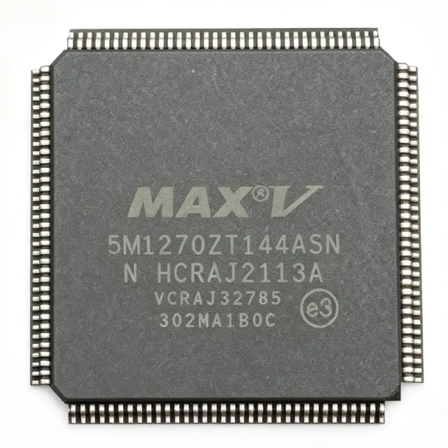
5M1270ZT144C5N - MAX V CPLD 980 Macrocells 114 I/O TQFP-144 | Intel / Altera
5M1270ZT144C5N ✓ 量产中规格对比
| 参数 | 5M1270ZT144A5N | 5M1270ZT144C5N |
|---|---|---|
| 品牌 | Intel | Altera |
| 分类 | FPGA & CPLD | FPGA & CPLD |
| 生命周期状态 | 有效 | 有效 |
| 库存状态 | 有库存 | 有库存 |
| 单价(USD) | $19.85 | $12.45 |
| Family | MAX V | — |
| Device Type | CPLD (Complex Programmable Logic Device) | CPLD (Complex Programmable Logic Device) |
| Macro Cells | 980 | — |
| User I/Os | 114 | 114 |
| Logic Elements | 2120 (approx.) | 1270 |
| User Flash Memory | 8 Kbits | — |
| Maximum Operating Frequency | 201.1 MHz | — |
| Speed Grade | 5N | — |
| Core Supply Voltage | 1.8 V | — |
| I/O Bank Voltage Support | 1.8 V / 2.5 V / 3.3 V / 5.0 V (MultiVolt) | — |
| 封装 | TQFP-144 (T144) | TQFP-144 (22 x 22 mm, 0.5 mm pitch) |
| 安装类型 | Surface Mount | Surface Mount |
| Process Technology | Non-volatile flash CMOS | — |
| Programming Interface | JTAG (IEEE 1149.1) | JTAG in-system programmable (Altera Quartus II) |
| Design Software | Quartus II / Quartus Prime | — |
| 工作温度 | -40C to +125C (automotive) | 0 C to +85 C (commercial grade) |
| Automotive Qualification | AEC-Q100 | — |
| RoHS 状态 | Compliant | Compliant |
| Internal Features | Pull-up resistors, bus-hold, on-chip oscillator | — |
| Series | — | MAX V |
| Macrocells | — | 980 |
| Maximum Internal Frequency | — | 118.3 MHz |
| Pin-to-Pin Propagation Delay (tPD) | — | 6.2 ns |
| Internal Frequency (typical) | — | 201 MHz |
| User Flash Memory (UFM) | — | 8 Kbits |
| Configuration Memory | — | Flash (non-volatile, in-system programmable) |
| VCCINT (Core Supply) | — | 1.71 V to 1.89 V |
| VCCIO (I/O Supply, per bank) | — | 1.2 V to 3.3 V |
| Number of I/O Banks | — | 4 |
| Supported I/O Standards | — | LVCMOS, LVTTL, PCI up to 3.3 V, 1.2 V to 3.3 V LVCMOS on JTAG pins |
| JTAG Interface | — | IEEE 1149.1 (TMS, TDI, TDO, TCK in Bank 1) |
| Program/Erase Cycles | — | Up to 100,000 |