XC7A100T-2CSG324I vs XC7A100T-L2CSG324E 对比
详细并排对比 XC7A100T-2CSG324I 出自 AMD 和 XC7A100T-L2CSG324E 出自 AMD。对比关键规格、电气参数、封装、生命周期状态、价格和供货情况,以确定最适合您设计需求的元器件。
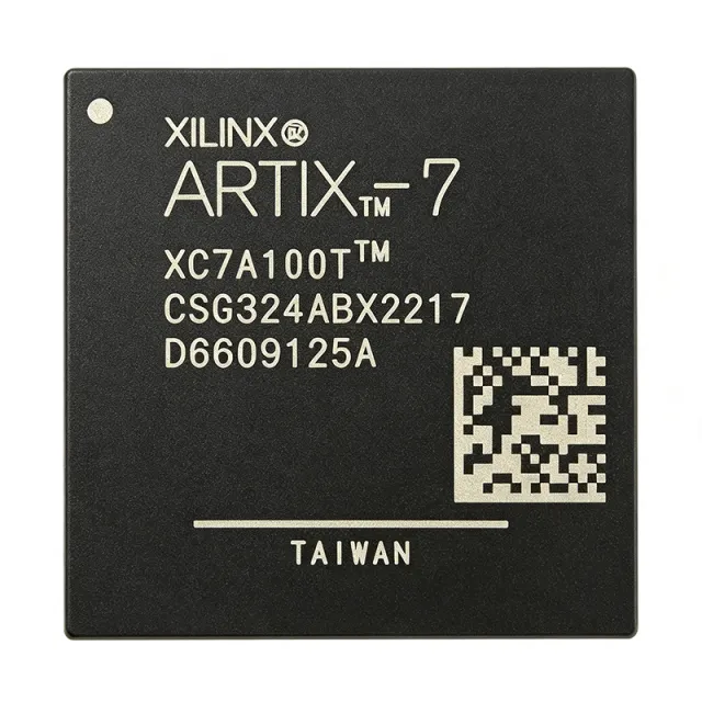

规格对比
| 参数 | XC7A100T-2CSG324I | XC7A100T-L2CSG324E |
|---|---|---|
| 品牌 | AMD | AMD |
| 分类 | FPGA & CPLD | FPGA & CPLD |
| 生命周期状态 | 有效 | 有效 |
| 单价(USD) | $105.00 | — |
| Family | Artix-7 | — |
| Number of Logic Elements/Cells | 101440 | — |
| Number of LABs/CLBs | 7925 | — |
| Total RAM Bits | 4976640 | — |
| Number of I/O | 210 | — |
| Number of DSP Slices | 240 | — |
| Number of Block RAM Blocks | 135 (36 Kb each) | — |
| Number of Flip-Flops | 285120 | — |
| Number of GTP Transceivers | 16 (up to 6.6 Gbps) | — |
| 工作电源电压 | 0.95 V ~ 1.05 V | — |
| 工作温度范围 | -40°C ~ +100°C (TJ) | — |
| 封装 | 324-LFBGA, CSPBGA (CSG324) | 324-terminal FC-BGA (CSG324) |
| 安装类型 | Surface Mount | Surface mount |
| Speed Grade | -2 | -L2 |
| Internal Clock Speed | Up to 628 MHz | — |
| Process Technology | 28 nm HKMG | 28 nm |
| Configuration Interface | JTAG, SelectMAP, Quad-SPI | — |
| XADC | 12-bit, 1 MSPS | — |
| PCIe Support | Gen2 x1 | — |
| Ethernet Support | 10/100/1000 Mbps | — |
| FPGA Family | — | Artix-7 |
| Logic Cells | — | 101,440 cells |
| Block RAM | — | 4,860 Kb |
| DSP Slices | — | 240 slices |
| Operating Voltage Class | — | 1 V |
| Terminal Count | — | 324 terminals |
| Temperature Grade | — | Extended, E grade |
| Junction Temperature Range | — | 0°C to 100°C |
| Programmable Logic Type | — | FPGA |
| On-Chip RAM | — | 4,860 Kb block RAM |
| Digital Signal Processing | — | 240 DSP slices |
| Configuration Memory | — | [DATA_NEEDED: configuration memory type and capacity] |
| Maximum I/O Count | — | [DATA_NEEDED: maximum user I/O count] |
| RoHS Compliance | — | [DATA_NEEDED: RoHS compliance status] |