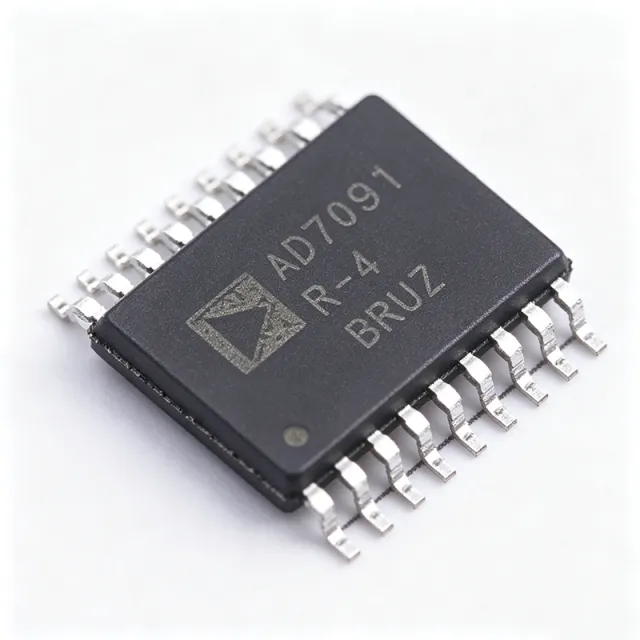
AD7091R-4BRUZ - 4-Ch 12-Bit 1MSPS SAR ADC | Analog Devices
料号: AD7091R-4BRUZ ✓ 量产中| 数量 | 单价 | 小计 |
|---|---|---|
| 1 | $4.5 | $4.50 |
| 10 | $4.05 | $40.50 |
| 100 | $3.6 | $360.00 |
| 500 | $3.24 | $1,620.00 |
| 1,000 | $3.04 | $3,040.00 |
AD7091R-4BRUZ 概述
An ADC (analog-to-digital converter) is a device that converts continuous analog signals into discrete digital numbers. The AD7091R-4BRUZ is a SAR ADC, which uses a binary search algorithm to determine the digital output. SAR ADCs are known for their high speed, low power, and ease of use, making them ideal for a wide range of applications. The AD7091R-4BRUZ is part of the AD7091R family, which includes 2-, 4-, and 8-channel versions, all sharing the same core architecture.
Key features of the AD7091R-4BRUZ include ultralow power consumption: normal mode draws only 1.4 mW at 1 MSPS, and power-down mode draws 550 nA typical at VDD = 5.25 V and 435 nA at VDD = 3 V. The device also features a programmable ALERT interrupt pin (on 4- and 8-channel models) for monitoring out-of-range conditions. The on-chip 2.5 V reference eliminates the need for an external reference, simplifying design.
The AD7091R-4BRUZ uses a flexible power/throughput rate management scheme, allowing the conversion rate to be adjusted to match the system's needs, thereby optimizing power consumption. The SPI interface supports data read after conversion, achieving a 1 MSPS throughput rate. The device also includes a channel sequencer that allows preprogrammed selection of channels to be converted sequentially, reducing microcontroller overhead.
Typical applications include battery-powered instrumentation, portable medical devices, industrial process control, and data acquisition systems. The low power consumption and small package make it ideal for portable and battery-operated equipment.
When designing with the AD7091R-4BRUZ, ensure that the analog input voltage does not exceed the supply voltage to avoid damage. Use a low-pass filter on the analog inputs to reduce noise and aliasing. The reference voltage is internally generated, but an external reference can be used if higher accuracy is required.
直接替换替代料: AD7091R-4BRUZ ——相同封装,引脚兼容。需要 PCB 改动的不同封装料号已排除。
本系列中的变体
可与以下型号直接替换的同系列型号: AD7091R-4BRUZ (相同外形与封装尺寸) ——差异在于 Interface, Number of Channels, Package, Sampling Rate, Internal Reference.
快速对比工具——选择替代料号进行并排对比:
AD7091R-2BRUZ
✅ 直接替换✓ 有现货
$1.83 / 个
查看数据手册 →AD7091R-5BRUZ-RL7
✅ 直接替换 ⚠️ 规格未核验✓ 有现货
$5.6 / 个
查看数据手册 →AD7091R-1BRUZ
✅ 直接替换 ⚠️ 规格未核验📋 参考替代料(不在目录中)
AD7091R-4BRUZ-RL7
✅ 直接替换📋 参考替代料(不在目录中)
AD7091R-4BRUZ 最大额定值与电气特性
| 分辨率 | 12 bits |
| Number of Channels | 4 |
| 采样率 | 1 MSPS |
| Input Type | Single-ended |
| Supply Voltage Range | 2.7 V to 5.25 V |
| 基准电压 | 2.5 V (internal) |
| Power Consumption (Normal Mode) | 1.4 mW at 1 MSPS |
| Power-Down Current (VDD = 5.25 V) | 550 nA typical |
| Power-Down Current (VDD = 3 V) | 435 nA typical |
| 接口 | SPI |
| 封装 | 20-lead TSSOP |
| 工作温度范围 | -40°C to +125°C |
| 安装类型 | Surface Mount |
| RoHS 状态 | Compliant |
| ALERT Pin | Yes (programmable) |
AD7091R-4BRUZ 引脚配置
| 引脚 1 | VDD — Power supply input, 2.7 V to 5.25 V |
| 引脚 2 | VIN0 — Analog input channel 0 |
| 引脚 3 | VIN1 — Analog input channel 1 |
| 引脚 4 | VIN2 — Analog input channel 2 |
| 引脚 5 | VIN3 — Analog input channel 3 |
| 引脚 6 | GND — Ground |
| 引脚 7 | SCLK — Serial clock input |
| 引脚 8 | DIN — Serial data input |
| 引脚 9 | DOUT — Serial data output |
| 引脚 10 | CS — Chip select (active low) |
| 引脚 11 | ALERT — Programmable alert output |
| 引脚 12 | CONVST — Conversion start input |
典型应用
AD7091R-4BRUZ 适用于 6 应用s: Battery-Powered Instrumentation, Portable Medical Devices, Industrial Process Control, Data Acquisition Systems, IoT and Smart Sensors, Test and Measurement Equipment.
Battery-Powered Instrumentation
The AD7091R-4BRUZ's ultralow power consumption (1.4 mW at 1 MSPS, 550 nA power-down) makes it ideal for battery-powered instruments. Its 2.7 V to 5.25 V supply range allows direct operation from a single lithium-ion cell or two alkaline batteries. The internal 2.5 V reference eliminates external components, saving board space and power. The SPI interface enables low-power microcontrollers to read data efficiently, extending battery life in portable multimeters, data loggers, and handheld analyzers.
推荐
Portable Medical Devices
In portable medical devices like glucose monitors and pulse oximeters, the AD7091R-4BRUZ provides high accuracy (12-bit) with minimal power draw. Its small 20-lead TSSOP package fits compact designs. The channel sequencer allows sequential sampling of multiple biosignals without microcontroller intervention, reducing firmware complexity. The ALERT pin can signal out-of-range conditions, enabling immediate patient alerts. Its low power-down current (435 nA at 3 V) is critical for devices that spend most time in standby.
推荐
Industrial Process Control
The AD7091R-4BRUZ is well-suited for industrial process control, where it monitors 4-20 mA loops, temperature sensors, and pressure transducers. Its 1 MSPS sampling rate enables fast response to process changes. The SPI interface allows easy integration with industrial microcontrollers and PLCs. The device's wide supply range (2.7 V to 5.25 V) accommodates various industrial power rails. The internal reference ensures stable conversions over temperature, critical for accurate control. The ALERT pin can trigger alarms when process variables exceed setpoints.
推荐
Data Acquisition Systems
In data acquisition systems, the AD7091R-4BRUZ offers a balance of speed (1 MSPS) and resolution (12-bit) for capturing dynamic signals. Its four channels can sample multiple sensors simultaneously using the channel sequencer. The SPI interface supports high-speed data transfer to FPGAs or DSPs. The ultralow power is advantageous in distributed DAQ nodes powered over Ethernet or battery. The internal reference simplifies design, and the small package allows high channel density on PCBs. The ALERT pin can be used for threshold detection, reducing host processor load.
推荐
IoT and Smart Sensors
The AD7091R-4BRUZ is ideal for IoT and smart sensor nodes that require low power and small size. Its 1 MSPS sampling rate is sufficient for many environmental sensors (temperature, humidity, gas). The power-down mode (550 nA) allows the ADC to be shut down between readings, conserving battery. The SPI interface connects easily to low-power MCUs like the ARM Cortex-M series. The internal reference reduces BOM count, and the 20-lead TSSOP is suitable for compact PCB designs. The channel sequencer enables periodic sampling of multiple sensors with minimal MCU involvement.
推荐
Test and Measurement Equipment
In test and measurement equipment, the AD7091R-4BRUZ provides accurate, high-speed digitization for oscilloscopes, spectrum analyzers, and data loggers. Its 12-bit resolution and 1 MSPS sampling rate capture transient signals with good fidelity. The four channels allow simultaneous monitoring of multiple test points. The SPI interface enables fast data transfer to processors for real-time analysis. The ultralow power is beneficial in portable test instruments. The internal reference ensures consistent measurements across units, and the ALERT pin can be used for trigger functions.
推荐
推荐产品汇总
工程参考数据: AD7091R-4BRUZ ——对比、设计指导和合规信息。
选型指南
与替代料对比
| 参数 | 本产品 | AD7091R-2BRUZ | AD7091R-8BRUZ | AD7091R-5BRUZ-RL7 |
|---|---|---|---|---|
| Package | 20-lead TSSOP | 20-lead TSSOP | 24-lead TSSOP | 20-lead TSSOP |
| Brand | Analog Devices | Analog Devices | Analog Devices | Analog Devices |
| Number of Channels | 4 | 2 | 8 | 5 |
| Sampling Rate | 1 MSPS | 1 MSPS | 1 MSPS | 1 MSPS |
| Supply Voltage Range | 2.7 V to 5.25 V | 2.7 V to 5.25 V | 2.7 V to 5.25 V | 2.7 V to 5.25 V |
| Power Consumption (Normal Mode) | 1.4 mW at 1 MSPS | 1.4 mW at 1 MSPS | 1.4 mW at 1 MSPS | 1.4 mW at 1 MSPS |
| Internal Reference | Yes (2.5 V) | Yes (2.5 V) | Yes (2.5 V) | Yes (2.5 V) |
| ALERT Pin | Yes | No | Yes | Yes |
关键差异点
- Ultralow power consumption (对比 AD7091R-2BRUZ)
- Internal 2.5 V reference (对比 AD7091R-8BRUZ)
- Programmable ALERT pin (对比 AD7091R-2BRUZ)
设计说明
The AD7091R-4BRUZ consumes only 1.4 mW at 1 MSPS, but power scales with throughput. Use the power-down mode (550 nA at 5.25 V, 435 nA at 3 V) between conversions to minimize average power. Ensure the supply voltage is within 2.7 V to 5.25 V and decouple VDD with a 0.1 µF ceramic capacitor close to the pin.
Place the ADC close to the signal source to minimize trace length and noise pickup. Use a ground plane under the device and route analog inputs away from digital traces. Add a low-pass filter (e.g., RC) on each analog input to reduce aliasing and high-frequency noise. Keep the SPI lines short and matched to avoid signal integrity issues.
Do not exceed the analog input voltage range (0 V to VDD) to avoid damaging the ADC. Ensure the reference voltage is stable; the internal 2.5 V reference is accurate, but for higher accuracy, an external reference can be used. The CONVST pin must be properly timed to achieve 1 MSPS; refer to the datasheet timing diagram. Avoid floating unused analog inputs; tie them to GND or VDD.
合规信息
RoHS compliant per Analog Devices product page. No AEC-Q100 qualification indicated for this part.






