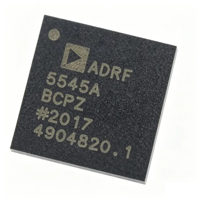
ADRF5545ABCPZN - Dual-Channel 2.4-4.2GHz RF Front End | Analog Devices
料号: ADRF5545ABCPZN ✓ 量产中| 数量 | 单价 | 小计 |
|---|---|---|
| 1 | $25.43 | $25.43 |
| 10 | $23.12 | $231.20 |
| 100 | $20.81 | $2,081.00 |
| 500 | $18.5 | $9,250.00 |
| 1,000 | $16.19 | $16,190.00 |
ADRF5545ABCPZN 概述
An RF front end (LNA + PA) is a critical component in wireless transceivers that conditions the signal between the antenna and the baseband processor. It typically includes a low-noise amplifier (LNA) to boost weak received signals with minimal added noise, and a power amplifier (PA) to amplify transmitted signals to the required power level. The ADRF5545A integrates these functions in a dual-channel configuration, enabling MIMO and diversity schemes in TDD systems.
Key features of the ADRF5545ABCPZN include dual-channel operation, wide frequency coverage from 2.4 GHz to 4.2 GHz, and integration of LNA and PA in a single module. The device is designed for TDD applications, where transmit and receive paths share the same frequency band but are time-multiplexed. The multichip module architecture ensures high isolation between channels and optimized performance for both receive and transmit paths.
Technically, the ADRF5545A employs advanced RF design techniques to achieve low noise figure in the receive path and high linearity in the transmit path. The dual-channel configuration supports 2x2 MIMO systems, improving data throughput and link reliability. The module is housed in a 40-lead LFCSP-VQ package with an exposed pad for thermal management, ensuring reliable operation in high-power transmit scenarios.
Typical applications include 5G NR TDD base stations, small cells, repeaters, and other wireless infrastructure equipment operating in the 2.4 GHz to 4.2 GHz band. The device is also suitable for point-to-point microwave links and radar systems that require compact, high-performance RF front ends.
When designing with the ADRF5545ABCPZN, careful attention must be paid to PCB layout to minimize parasitic inductance and ensure proper grounding. The exposed pad should be soldered to a thermal via array to dissipate heat effectively. Additionally, the TDD switching control must be synchronized with the system timing to avoid signal leakage between transmit and receive paths.
直接替换替代料: ADRF5545ABCPZN ——相同封装,引脚兼容。需要 PCB 改动的不同封装料号已排除。
本系列中的变体
可与以下型号直接替换的同系列型号: ADRF5545ABCPZN (相同外形与封装尺寸) ——差异在于 Frequency Range.
快速对比工具——选择替代料号进行并排对比:
ADRF5545ABCPZN-R7
📋 参考替代料(不在目录中)
ADRF5545ABCPZ
📋 参考替代料(不在目录中)
ADRF5545ABCPZN-R7
📋 参考替代料(不在目录中)
ADRF5545ABCPZ
📋 参考替代料(不在目录中)
ADRF5545ABCPZN-R7
📋 参考替代料(不在目录中)
ADRF5545ABCPZN 规格参数
| Frequency Range | 2.4 GHz to 4.2 GHz |
| Number of Channels | 2 |
| Type | RF Front End (LNA + PA) |
| 封装 | 40-LFCSP-VQ (6x6 mm) |
| 安装类型 | Surface Mount |
| RoHS 状态 | Compliant |
ADRF5545ABCPZN 引脚配置
| 引脚 1 | GND — Ground |
| 引脚 2 | RF1_IN — RF input for channel 1 |
| 引脚 3 | GND — Ground |
| 引脚 4 | RF1_OUT — RF output for channel 1 |
| 引脚 5 | GND — Ground |
| 引脚 6 | VCC1 — Supply voltage for channel 1 |
| 引脚 7 | GND — Ground |
| 引脚 8 | TDD_SW — TDD switching control |
| 引脚 9 | GND — Ground |
| 引脚 10 | VCC2 — Supply voltage for channel 2 |
| 引脚 11 | GND — Ground |
| 引脚 12 | RF2_OUT — RF output for channel 2 |
| 引脚 13 | GND — Ground |
| 引脚 14 | RF2_IN — RF input for channel 2 |
| 引脚 15 | GND — Ground |
| 引脚 16 | NC — No connect |
| 引脚 17 | GND — Ground |
| 引脚 18 | NC — No connect |
| 引脚 19 | GND — Ground |
| 引脚 20 | NC — No connect |
典型应用
ADRF5545ABCPZN 适用于 6 应用s: 5G NR TDD Base Stations, Small Cells and Repeaters, Point-to-Point Microwave Links, Radar Systems, Wireless Infrastructure, Test and Measurement Equipment.
5G NR TDD Base Stations
The ADRF5545ABCPZN is ideal for 5G NR TDD base stations operating in the 2.4-4.2 GHz band. Its dual-channel configuration supports 2x2 MIMO, and the integrated LNA and PA reduce board space and design complexity. The module's TDD switching capability ensures reliable time-division duplexing, while its high linearity and low noise figure maintain signal integrity in dense urban environments. By integrating both transmit and receive paths, the ADRF5545A simplifies the RF front-end design, enabling faster time-to-market for 5G infrastructure.
推荐
Small Cells and Repeaters
For small cells and repeaters, the ADRF5545ABCPZN provides a compact, integrated RF front end that fits within tight form factors. Its 6x6 mm LFCSP package and dual-channel capability enable high-density designs, while the integrated LNA and PA eliminate the need for external matching networks. The module's wide frequency range covers multiple bands, making it versatile for multi-band small cell deployments. Its low power consumption and thermal efficiency are critical for outdoor installations where heat dissipation is limited.
推荐
Point-to-Point Microwave Links
The ADRF5545ABCPZN is suitable for point-to-point microwave links operating in the 2.4-4.2 GHz band. Its dual-channel architecture supports frequency diversity and MIMO, enhancing link reliability. The integrated LNA provides low noise figure, improving receiver sensitivity, while the PA delivers sufficient output power for medium-range links. The module's TDD capability allows efficient use of the spectrum, and its compact package simplifies integration into outdoor units.
推荐
Radar Systems
In radar systems, the ADRF5545ABCPZN offers a dual-channel RF front end that can be used for transmit/receive modules in phased array radars. Its wide frequency range covers C-band and part of S-band, making it suitable for various radar applications. The integrated LNA and PA reduce component count and improve reliability, while the TDD switching supports pulsed operation. The module's high linearity ensures accurate signal processing, and its compact size enables dense array configurations.
推荐
Wireless Infrastructure
The ADRF5545ABCPZN is a key component in wireless infrastructure, including distributed antenna systems (DAS) and remote radio heads (RRH). Its dual-channel design supports MIMO and diversity, improving network capacity and coverage. The integrated RF front end reduces the number of discrete components, lowering BOM cost and board space. The module's performance is optimized for TDD systems, ensuring efficient spectrum utilization. Its robust design meets the reliability requirements of infrastructure equipment.
推荐
Test and Measurement Equipment
In test and measurement equipment, the ADRF5545ABCPZN can be used as a building block for RF signal generation and analysis. Its dual-channel capability allows simultaneous measurement of multiple signals, improving test throughput. The integrated LNA and PA provide a complete front-end solution for RF test instruments, reducing design effort. The module's wide frequency range covers common test bands, and its high linearity ensures accurate measurements. The compact package is ideal for portable test equipment.
推荐
推荐产品汇总
工程参考数据: ADRF5545ABCPZN ——对比、设计指导和合规信息。
选型指南
与替代料对比
| 参数 | 本产品 | ADRF5545ABCPZN-R7 | ADRF5545ABCPZ |
|---|---|---|---|
| Package | 40-LFCSP-VQ (6x6) | 40-LFCSP-VQ (6x6) | 40-LFCSP-VQ (6x6) |
| Brand | Analog Devices | Analog Devices | Analog Devices |
| Frequency Range | 2.4 GHz to 4.2 GHz | 2.4 GHz to 4.2 GHz | 2.4 GHz to 4.2 GHz |
| Number of Channels | 2 | 2 | 2 |
| Type | RF Front End (LNA + PA) | RF Front End (LNA + PA) | RF Front End (LNA + PA) |
| Mounting Type | Surface Mount | Surface Mount | Surface Mount |
| RoHS Status | Compliant | Compliant | Compliant |
| Packaging | Tape & Reel | Tape & Reel | Tray |
关键差异点
- Dual-channel integrated RF front end (对比 Discrete LNA and PA solutions)
- Wide frequency coverage (对比 Narrowband RF front ends)
- TDD-optimized design (对比 FDD RF front ends)
设计说明
Ensure proper grounding and thermal management. The exposed pad of the 40-LFCSP-VQ package must be soldered to a ground plane with multiple thermal vias to dissipate heat effectively. Follow the layout guidelines in the ADRF5545A datasheet for optimal RF performance.
Keep RF traces as short as possible and use controlled impedance transmission lines (e.g., 50 ohms) for RF1_IN, RF1_OUT, RF2_IN, and RF2_OUT. Maintain adequate spacing between RF lines and digital control lines to minimize coupling.
Ensure the TDD_SW pin is properly synchronized with the system timing to prevent signal leakage between transmit and receive paths. Incorrect switching can degrade performance and cause spurious emissions.
合规信息
RoHS compliant per distributor listings. Other compliance data not specified in provided sources.






