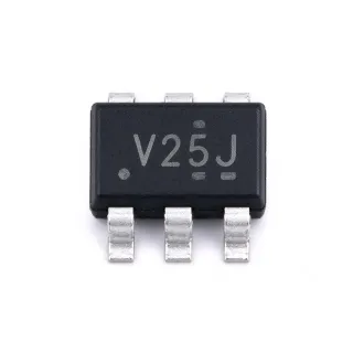
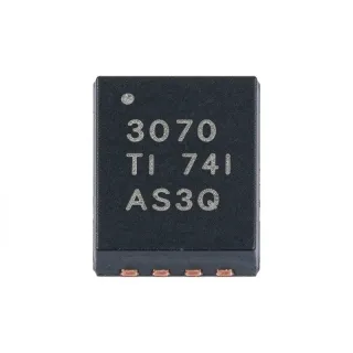
CD4502BM - 6-Channel 3-18V CMOS Inverter | Texas Instruments
料号: CD4502BM ✓ 量产中CD4502BM 概述
A CMOS hex inverter/buffer is a logic-family device that combines inversion with controlled output impedance. The CD4502B belongs to the broader hierarchy of CMOS logic, logic buffer or driver, interface IC, and digital semiconductor. Its high-impedance output state allows multiple channels to share a common data bus without active drive contention, while its low-noise-margin operating limits define the voltage range in which attached CMOS circuitry is reliably interpreted.
Key features include six independently buffered inverter channels, three-state outputs, a common output-disable input, and a common inhibit input. A logic 1 on OUTPUT DISABLE places all six outputs in the high-impedance state. A logic 1 on INHIBIT drives all six outputs to logic 0 when OUTPUT DISABLE is low. According to the Texas Instruments product page, the device can drive two standard TTL loads, equivalent to six times the JEDEC B-series IOL standard.
The CD4502B follows the JEDEC B-series CMOS framework and operates across a 3 V to 18 V supply range. CMOS construction provides high input impedance and low static supply demand, while the buffered push-pull output configuration supports dependable drive into compatible logic loads. The three-state function is especially useful for bidirectional or shared-bus arrangements where multiple devices must be electrically isolated while disabled.
Typical uses include CMOS-to-TTL interfacing, data-bus isolation, instrument control, industrial automation, embedded control, and digital signal conditioning. The common disable and inhibit functions allow a system controller to place an entire six-channel group into a safe state or force the group to logic 0, reducing external control logic and simplifying fault handling.
The primary design consideration is logic-level compatibility. Supply voltage, input thresholds, fanout, and the enabled or disabled state of every driver must be checked before connecting outputs to a shared bus. Unconnected inputs should not be left floating, and supply bypassing should follow the manufacturer's recommended layout to limit transient noise during output state changes.
This product record combines verified manufacturer and distributor information, a pin-compatible alternative review, application guidance, and design-specific cautions. It is intended to help engineers identify the correct logic function, verify package compatibility, and implement the CD4502BM without relying only on a distributor parameter summary.
直接替换替代料: CD4502BM ——相同封装,引脚兼容。需要 PCB 改动的不同封装料号已排除。
CD4502BMSR
✅ 直接替换📋 参考替代料(不在目录中)
CD4502BNSR
✅ 直接替换📋 参考替代料(不在目录中)
HEF4502BT
✅ 直接替换📋 参考替代料(不在目录中)
CD4502BM 最大额定值与电气特性
| Product Type | CMOS strobed hex inverter/buffer with 3-state outputs |
| Number of Channels | 6 channels |
| Number of Elements | 6 elements |
| Bits per Element | 1 bit per element |
| Logic Type | Inverting buffer |
| 输出类型 | Push-pull, 3-state |
| Supply Voltage Range | 3 V to 18 V |
| Noise Margin at 5 V | 1 V |
| Noise Margin at 10 V | 2 V |
| Noise Margin at 15 V | 2.5 V |
| TTL Drive Capability | 2 standard TTL loads, equivalent to 6 times the JEDEC B-series IOL standard |
| Output Disable Control | Logic 1 disables all six outputs into the high-impedance state |
| Inhibit Control | Logic 1 forces all six outputs to logic 0 when output disable is low |
| 封装 | 16-pin SOIC |
| 安装类型 | Surface mount |
| 工作温度 | -55 °C to +125 °C |
| Technology Standard | JEDEC Tentative Standard No. 13B for B-series CMOS devices |
CD4502BM 16-pin soic 引脚配置指南
CD4502BM(16-pin soic 封装)的引脚配置。 该数字 IC 包含 GPIO、通信接口(UART、SPI、I2C)和电源引脚。请参阅制造商数据手册以了解复用引脚功能和配置选项。对嵌入式系统设计和 PCB 布局至关重要。

暂无详细引脚数据: CD4502BM.
请参阅 数据手册 以查看完整引脚配置。
典型应用
CD4502BM 适用于 6 应用s: CMOS-to-TTL Data-Bus Interface, Shared Bidirectional Data Bus, Industrial Control Signal Conditioning, Digital Instrumentation Control, Embedded Logic Fan-Out, Digital Signal Fault Containment.
CMOS-to-TTL Data-Bus Interface
The CD4502BM fits a CMOS-to-TTL interface because its six inverting channels can convert a group of CMOS signals while driving up to two standard TTL loads. According to the Texas Instruments product page, this equals six times the JEDEC B-series IOL standard. A 3 V to 18 V supply range supports both low-voltage CMOS systems and higher-voltage legacy logic. The common OUTPUT DISABLE input can place all six outputs in the high-impedance state when the interface must be disconnected. Designers should still verify the output levels at the selected supply voltage and the input thresholds of the attached TTL devices.
推荐
Shared Bidirectional Data Bus
The CD4502BM is appropriate for a shared data bus because a logic 1 on OUTPUT DISABLE releases all six outputs to the high-impedance state. This prevents active output contention when another bus driver becomes active. The six-channel organization also reduces the number of discrete interface circuits required in a parallel bus. Its push-pull outputs provide defined drive when enabled, while the common inhibit control can force the group to logic 0 for a controlled inactive state. System timing must ensure output-disable and enable intervals do not overlap when two devices share the same nodes.
推荐
Industrial Control Signal Conditioning
The CD4502BM can condition six control signals in industrial logic systems that require inversion and bus isolation. Its common OUTPUT DISABLE and INHIBIT inputs simplify group-level fault handling: disable isolates the channels, while inhibit forces all outputs to logic 0. The verified operating-temperature range of -55 °C to +125 °C supports applications across a wide environmental range, subject to the complete system's qualification requirements. Engineers should validate voltage levels at every connected controller and include suitable input tie-offs for unused channels according to the official data sheet.
推荐
Digital Instrumentation Control
The CD4502BM is useful in test and measurement equipment where multiple digital control lines must be inverted, buffered, or electrically isolated from a common bus. Its 3 V to 18 V operating range allows use with different supply domains within an instrument, subject to level compatibility at each interface. The OUTPUT DISABLE function supports measurement-system isolation between active and inactive circuit sections. Compared with six discrete inverters, the common controls reduce routing overhead and provide a coordinated way to disable or force the entire group.
推荐
Embedded Logic Fan-Out
The CD4502BM can provide six buffered, inverted outputs from six input signals in an embedded control system. CMOS input impedance makes the device suitable for interfacing higher-impedance control sources, while the push-pull outputs provide active drive for compatible logic loads. The 1 V noise margin at 5 V is particularly relevant when the surrounding system operates at 5 V. The three-state capability allows the outputs to be removed from a shared line during transitions. Layout should place supply bypassing close to the device and maintain short output paths to minimize switching transients.
推荐
Digital Signal Fault Containment
The CD4502BM can support fault containment by using INHIBIT to force all six outputs to logic 0 and OUTPUT DISABLE to place the outputs in a high-impedance state. These two controls provide distinct protective behaviors when an upstream controller detects an abnormal condition. The common architecture allows one safety-oriented control signal to manage an entire channel group. Designers should establish which state is safest for the connected load, verify that no other driver remains active on a shared bus, and ensure the control logic cannot switch OUTPUT DISABLE and INHIBIT into an unintended combination.
推荐
推荐产品汇总
工程参考数据: CD4502BM ——对比、设计指导和合规信息。
选型指南
与替代料对比
| 参数 | 本产品 | CD4502BMSR | CD4502BNSR | HEF4502BT |
|---|---|---|---|---|
| Package | 16-SOIC | 16-SOIC - same | 16-SOIC - same | 16-SOIC - same |
| Brand | Texas Instruments | Texas Instruments | Texas Instruments | NXP Semiconductors |
| Product Type | CMOS strobed hex inverter/buffer with 3-state outputs | CMOS strobed hex inverter/buffer with 3-state outputs | CMOS strobed hex inverter/buffer with 3-state outputs | CMOS hex inverter/buffer with 3-state outputs |
| Number of Channels | 6 channels | 6 channels | 6 channels | 6 channels |
| Logic Function | Inverting | Inverting | Inverting | Inverting |
| Output State | Push-pull with 3-state output | Push-pull with 3-state output | Push-pull with 3-state output | 3-state output |
| Supply Voltage Range | 3 V to 18 V | 3 V to 18 V | 3 V to 18 V | 3 V to 18 V |
| Output Disable | Logic 1 produces high impedance on all outputs | Logic 1 produces high impedance on all outputs | Logic 1 produces high impedance on all outputs | Logic 1 produces high impedance on all outputs |
关键差异点
- Collective six-channel bus isolation (对比 CD4502BMSR)
- Distinct disable and forced-zero states (对比 CD4502BNSR)
- Cross-brand source consolidation (对比 HEF4502BT)
设计说明
Treat OUTPUT DISABLE and INHIBIT as separate controls. OUTPUT DISABLE releases all six outputs to the high-impedance state, while INHIBIT forces all outputs to logic 0 only when OUTPUT DISABLE is low. Before connecting multiple devices to one bus, define every legal control combination and ensure two drivers are never enabled on the same node at the same time.
The CD4502BM operates across 3 V to 18 V, but input thresholds and output levels vary with VDD. Confirm the logic-high and logic-low requirements of every attached device at the selected supply voltage. The verified noise margins are 1 V at 5 V, 2 V at 10 V, and 2.5 V at 15 V; do not assume those margins apply at every point in the supply range.
Place the device close to the signals it buffers and route output-disable and inhibit traces away from high-current switching nodes. Keep the supply and ground connections short, and follow the manufacturer's recommended decoupling arrangement in the official CD4502B data sheet. Good return paths and local bypassing reduce output transients that could affect neighboring CMOS circuitry.
Do not leave unused CMOS inputs floating. High input impedance does not make an open input harmless because leakage and internal transitions can create excessive current or unstable logic behavior. Apply the unused-input recommendations from the manufacturer data sheet, and use pull-up or pull-down arrangements that maintain a valid level whenever the associated control or data source is disconnected.
合规信息
The verified excerpts identify JEDEC Tentative Standard No. 13B compliance but do not provide RoHS, REACH, lead-free, halogen-free, conflict-minerals, or AEC-Q100 declarations. AEC-Q100 is marked not applicable because CD4502BM is a general-purpose logic IC rather than an automotive-qualified device.