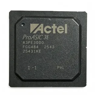
EP4CE15F23I8LN - 15K-LUT Cyclone IV E FPGA | Altera
料号: EP4CE15F23I8LN ✓ 量产中EP4CE15F23I8LN 概述
A Cyclone IV E FPGA belongs to the field-programmable gate array hierarchy, where programmable logic, fixed blocks, embedded memory, and general-purpose I/O are integrated into a reconfigurable semiconductor. Unlike a fixed-function application-specific integrated circuit, an FPGA permits designers to define parallel processing, control, and interface logic after manufacture. The EP4CE family is positioned for designs requiring substantial logic density without moving to a larger device family.
The EP4CE15F23I8LN provides 15,408 logic elements and uses a 1.2 V core supply. Its F23 package designation and 484-pin FBGA construction support dense board-level integration. The industrial-temperature ordering code makes the device relevant to equipment operating beyond commercial ambient conditions. The exact I/O standards, supported memory configurations, clock resources, and operating limits must be selected from the manufacturer ordering-part-number information and Cyclone IV E device documentation before schematic capture.
Its programmable architecture is useful for parallel datapaths, protocol bridges, control logic, and test systems. The 15,408-cell resource count allows multiple finite-state machines, counters, lookup logic, and interface channels to be consolidated in one device. Designers should map clocks, memories, and I/O standards against the exact F23 package tables because unused balls and supported voltage standards depend on the selected bank configuration.
Typical applications include industrial automation, communications equipment, instrumentation, embedded control, video or image processing, and general-purpose prototyping. The FPGA can implement parallel logic faster than a microcontroller for data movement and fixed pipelines, while retaining reprogrammability for product updates and design iteration. The 484-pin FBGA also requires careful escape routing, via-in-pad considerations, and thermal planning on multilayer boards.
Before placing the device on a PCB, assign every power ball to the appropriate supply rail, decouple each rail according to the manufacturer guidance, and route all configuration, reset, clock, and serial programming signals against the package-specific pin table. Validate the board with the same voltage, temperature, and programming procedure used in production because configuration pins, termination requirements, and bank power sequencing are critical to reliable operation.
This product record combines the exact ordering information, package identification, and available cross-reference candidates with application guidance, comparison criteria, and PCB-focused engineering notes. It is intended to support design selection and sourcing decisions while directing engineers to the authoritative device documentation for final electrical and pin-level verification.
直接替换替代料: EP4CE15F23I8LN ——相同封装,引脚兼容。需要 PCB 改动的不同封装料号已排除。
本系列中的变体
可与以下型号直接替换的同系列型号: EP4CE15F23I8LN (相同外形与封装尺寸) ——差异在于 Logic Elements, Mounting Type, Process Technology, Package Type.
EP4CE15F23I8L
✅ 直接替换联系询价
查看数据手册 →EP4CE15F23C8LN
✅ 直接替换联系询价
查看数据手册 →EP4CE15F23C8N
✅ 直接替换联系询价
查看数据手册 →EP4CE15F23I7LN
✅ 直接替换📋 参考替代料(不在目录中)
EP4CE115F23I7LN
✅ 直接替换📋 参考替代料(不在目录中)
EP4CE15F23I8LN 最大额定值与电气特性
| Device Type | Field Programmable Gate Array (FPGA) |
| FPGA Family | Cyclone IV E |
| Device Variant | EP4CE15 (F23) |
| Logic Cells / Logic Blocks | 47 |
| Logic Elements | 15,408 |
| 电源电压 | 1.2 V |
| Process Technology | 60 nm |
| Package Type | 484-FBGA |
| 引脚数量 | 256 pins |
| Total I/O | 214 |
| 工作温度范围 | Industrial temperature range |
| 安装类型 | Surface mount |
| Programmability | Reconfigurable FPGA |
EP4CE15F23I8LN 484-fbga 引脚配置指南
EP4CE15F23I8LN(484-fbga 封装)的引脚配置。 该数字 IC 包含 GPIO、通信接口(UART、SPI、I2C)和电源引脚。请参阅制造商数据手册以了解复用引脚功能和配置选项。对嵌入式系统设计和 PCB 布局至关重要。

暂无详细引脚数据: EP4CE15F23I8LN.
请参阅 数据手册 以查看完整引脚配置。
典型应用
EP4CE15F23I8LN 适用于 6 应用s: Industrial Automation Controllers, Communications Protocol Bridges, Precision Instrumentation, Machine Vision and Image Processing, Embedded Data Acquisition, Programmable Logic Prototyping.
Industrial Automation Controllers
The EP4CE15F23I8LN fits industrial automation controllers that need deterministic parallel logic alongside programmable interfaces. Its 15,408 logic elements can implement state machines, motor-control sequencing, interlocks, counters, and fieldbus data paths without relying on a chain of discrete logic devices. The 484-FBGA package supports a high pin count, while the 1.2 V core supply and 60 nm Cyclone IV E architecture provide a suitable platform for control, monitoring, and safety-adjacent logic partitioning. Engineers should use the exact F23 package tables to assign bank voltage standards and industrial I/O, and they should verify timing, temperature, and EMC requirements against the finished enclosure and connected sensors.
推荐
Communications Protocol Bridges
The EP4CE15F23I8LN is suitable for communications protocol bridges that must translate between serial interfaces, parallel data streams, and buffering functions. Its 15,408 logic elements allow multiple finite-state machines and datapaths to run concurrently, and the 214 available I/O provide connections for clocks, control signals, and parallel buses. A communications bridge can use dedicated logic for clock-domain crossing, packet framing, FIFO control, and error handling. The engineer must verify supported I/O standards and maximum clock rates for the exact F23 speed grade, then budget routing and timing margin in the Quartus design. Power planning should also ensure that the FPGA core and selected I/O banks remain within their specified limits.
推荐
Precision Instrumentation
The EP4CE15F23I8LN can implement measurement sequencing, calibration control, data acquisition formatting, and instrument communication in a compact FPGA subsystem. Its 15,408 logic elements are useful for parallel sampling pipelines, digital filters, trigger logic, and timestamp processing, while the 484-pin FBGA exposes a broad selection of user I/O. The exact F23 device tables should be used to select compatible voltage standards for analog front ends, memory interfaces, and laboratory controls. For precision applications, separate analog and digital ground-current paths, use controlled clock distribution, and analyze deterministic timing with the compiled design rather than relying only on device-family averages.
推荐
Machine Vision and Image Processing
The EP4CE15F23I8LN is applicable to machine-vision preprocessing when the FPGA must execute parallel pixel operations, thresholding, filtering, or frame timing in real time. Its 15,408 logic elements can support fixed pipelines that operate on multiple pixels per clock, while the 214 I/O provide flexible connectivity to image sensors, capture devices, memory, and downstream processors. The 484-FBGA package also allows direct assignment of parallel sensor, clock, and control signals. The design should establish timing constraints for the sensor and memory interfaces, verify supported I/O standards from the F23 package data, and verify the industrial temperature requirement. Power and thermal performance depend on the selected clock rate and logic utilization, so timing-driven compilation is essential.
推荐
Embedded Data Acquisition
The EP4CE15F23I8LN can act as the programmable acquisition engine in systems that collect multiple sensor channels and perform real-time filtering or buffering before transmission. Its 15,408 logic elements are suited to parallel ADC interfaces, digital decimation stages, threshold logic, and control of external memory. With 214 I/O, the device can support several acquisition channels plus clocks, triggers, status signals, and high-speed serial links. Correct implementation requires confirming the supported voltage standards and timing characteristics of every connected interface in the exact package documentation. The board layout should provide local decoupling, controlled clock routing, and adequate thermal spreading around the 484-FBGA, while the FPGA configuration path should be designed for reliable field updates.
推荐
Programmable Logic Prototyping
The EP4CE15F23I8LN supports general-purpose logic prototyping because its 15,408 logic elements, 214 I/O, and configurable architecture allow multiple test algorithms and interface behaviors to be changed in the field. Engineers can implement bus analyzers, protocol exercisers, timing generators, fault injectors, and accelerator prototypes on the same programmable platform. The industrial-temperature ordering option is useful when the prototype will operate in production-like environmental conditions. Development should begin with a verified board pinout, a stable configuration scheme, and JTAG access for programming and debugging. After routing is complete, the exact design should be analyzed for timing closure, power consumption, and thermal margin rather than relying on nominal logic-cell counts.
推荐
推荐产品汇总
工程参考数据: EP4CE15F23I8LN ——对比、设计指导和合规信息。
选型指南
与替代料对比
| 参数 | 本产品 | EP4CE15F23I8L | EP4CE15F23C8LN | EP4CE15F23C8N | EP4CE15F23I7LN | EP4CE115F23I7LN |
|---|---|---|---|---|---|---|
| Brand | Altera | Altera | Altera | Altera | Altera | Altera |
| Package | 484-FBGA | 484-FBGA | 484-FBGA | 484-FBGA | 484-FBGA | 484-FBGA |
| Device Family | Cyclone IV E | Cyclone IV E | Cyclone IV E | Cyclone IV E | Cyclone IV E | Cyclone IV E |
| Supply Voltage | 1.2 V | 1.2 V | 1.2 V | 1.2 V | 1.2 V | 1.2 V |
| Process Technology | 60 nm | 60 nm | 60 nm | 60 nm | 60 nm | 60 nm |
| Speed Grade | F23 standard grade | F23 standard grade | F23 standard grade | F23 standard grade | -7 faster speed grade | -7 faster speed grade |
关键差异点
- Exact industrial-temperature ordering identity within the EP4CE15 F23 family (对比 EP4CE15F23C8LN)
- Standard F23 speed grade avoids the power and thermal implications of an unnecessary speed upgrade (对比 EP4CE15F23I7LN)
- Exact EP4CE15 resource class with 15,408 logic elements (对比 EP4CE115F23I7LN)
- Package and terminal continuity with the closest ordering variant (对比 EP4CE15F23I8L)
设计说明
Create the PCB symbol directly from the F23 package pin table rather than from a generic EP4CE15 symbol. Assign every 484 ball, including power, ground, configuration, clock, and user I/O functions, and mark unused balls according to the manufacturer guidance. Run a package-versus-symbol audit before fabrication because an incorrect generic symbol can create both power-routing errors and I/O conflicts that are difficult to diagnose after assembly.
Plan separate core and I/O supply distributions with local high-frequency decoupling at the appropriate 1.2 V and bank supply pins. Follow the exact Cyclone IV E power-supply sequence, voltage limits, and decoupling recommendations for the selected bank standards. The device family can operate at 1.2 V, but the complete design also depends on I/O voltage, speed grade, utilization, and switching activity, so estimate both average and transient demand before selecting regulators.
Provide a thermal path for the 484-FBGA and spread high-speed return currents through nearby ground planes. Estimated power dissipation is (core voltage × core current) plus the I/O-bank power, but actual values depend on compilation, clocking, and I/O activity. Use the compiled Quartus power report for final analysis and check junction-temperature margin against the package thermal data rather than treating the nominal 1.2 V supply as the total device power.
Do not approve a replacement based only on the FPGA family and package. Verify configuration mode, active serial or parallel programming signals, power-up behavior, supported I/O standards, speed grade, temperature grade, and pin multiplexing. EP4CE15F23I8L is the closest ordering candidate, while C8 changes temperature class and I7 changes speed class. A PCB-compatible footprint does not by itself guarantee that the configuration flash, clocking, and system behavior remain identical.
Keep configuration traces short and route them away from high-slew current paths. Use a solid, continuous ground reference under and around the BGA, avoid splits beneath signal or power balls, and minimize via stubs when using high-speed interfaces. Match clock distribution and external memory routing to the compiled timing constraints. Since the exact F23 pin table and board stack-up determine the escape strategy, validate the layout with signal-integrity and power-integrity simulations before fabrication.
合规信息
The available comparison material mentions RoHS and REACH status, but no explicit declaration or material statement was supplied for this exact ordering part number. Confirm compliance and terminal-finish information using the manufacturer documentation for EP4CE15F23I8LN.