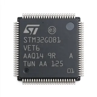
STM32F107VBT6 - 72MHz Cortex-M3 MCU | STMicroelectronics
料号: STM32F107VBT6 ✓ 量产中STM32F107VBT6 概述
A microcontroller is a programmable semiconductor that integrates a processor core, memory, and communication or control peripherals onto one device. Within the product hierarchy, the STM32F107VBT6 belongs to the ARM Cortex-M microcontroller family, within the broader embedded-processing and semiconductor categories. Its 32-bit Cortex-M3 core provides the architectural base for connected industrial equipment, network-interface controllers, gateways, and other embedded control systems.
The principal device characteristics are a 72 MHz operating frequency, 128 KB of Flash program memory, 32-bit processing, and a compact 100-pin LQFP package. The manufacturer identifies the part as part of the STM32F1 connectivity line. The verified distributor records also identify 2.5 V and 3.3 V supply options, making the device applicable to common embedded-system rail architectures when the complete electrical limits are confirmed in the manufacturer datasheet.
The 128 KB Flash capacity provides more room for firmware, protocol stacks, boot logic, and application code than many entry-level 32-bit microcontrollers. Its 72 MHz Cortex-M3 processing capability supports responsive control and communication tasks, while the 14 x 14 mm LQFP outline offers a fine-pitch surface-mount option for densely populated controller boards. The exact SRAM configuration, peripheral inventory, clock tree, and electrical limits should be checked against the STM32F107VB documentation before schematic capture.
Typical uses include industrial Ethernet equipment, communication gateways, embedded controllers, and network-interface modules. In such systems, the MCU can manage protocol processing, supervisory logic, and peripheral configuration while external interface ICs handle Ethernet PHY or USB transceiver functions. The 100-pin package provides a substantial pin count for mixed signal, control, and connectivity-oriented designs.
PCB design should account for the fine-pitch LQFP footprint, decoupling requirements, clock-signal integrity, and exposed programming or debug access. Confirm the exact pin assignments and alternate-function requirements in the manufacturer pinout and datasheet. Verify supply sequencing, operating-temperature limits, and peripheral electrical characteristics before releasing a production design.
This page consolidates the manufacturer identity, core device ratings, package information, pricing record, and documented cross-reference candidates. It also provides application guidance, design cautions, and a structured comparison framework to support component selection and PCB reuse decisions.
直接替换替代料: STM32F107VBT6 ——相同封装,引脚兼容。需要 PCB 改动的不同封装料号已排除。
本系列中的变体
可与以下型号直接替换的同系列型号: STM32F107VBT6 (相同外形与封装尺寸) ——差异在于 Package, Flash Memory, Timers.
STM32F107VBT7
✅ 直接替换📋 参考替代料(不在目录中)
STM32F105VBT6
✅ 直接替换 ⚠️ 规格未核验联系询价
查看数据手册 →STM32F103VBT7
✅ 直接替换 ⚠️ 规格未核验联系询价
查看数据手册 →GD32F107VBT6
✅ 直接替换📋 参考替代料(不在目录中)
GD32F103VBT6
✅ 直接替换📋 参考替代料(不在目录中)
STM32F107VBT6 最大额定值与电气特性
| Product Type | 32-bit ARM Cortex-M3 microcontroller |
| Processor Core | ARM Cortex-M3 |
| 最大时钟频率 | 72 MHz |
| Flash Memory | 128 KB |
| Flash Organization | 128K x 8 bits |
| Architecture | 32-bit RISC |
| Supply Voltage Options | 2.5 V or 3.3 V |
| 封装 | 100-pin LQFP |
| Package Body Size | 14 x 14 mm |
| Product Family | STM32F105xx and STM32F107xx connectivity line |
| 安装类型 | Surface mount |
STM32F107VBT6 14 x 14 mm 引脚配置指南
STM32F107VBT6(14 x 14 mm 封装)的引脚配置。 该数字 IC 包含 GPIO、通信接口(UART、SPI、I2C)和电源引脚。请参阅制造商数据手册以了解复用引脚功能和配置选项。对嵌入式系统设计和 PCB 布局至关重要。

暂无详细引脚数据: STM32F107VBT6.
请参阅 数据手册 以查看完整引脚配置。
典型应用
STM32F107VBT6 适用于 6 应用s: Industrial Ethernet Gateways, Network Interface Modules, Industrial Control Boards, Communication Equipment, Embedded Data Acquisition Systems, Secure Network-Adjacent Controllers.
Industrial Ethernet Gateways
The STM32F107VBT6 fits industrial Ethernet gateways that require a 72 MHz Cortex-M3 processor, 128 KB of embedded Flash, and a high pin count in a 14 x 14 mm LQFP package. Its connectivity-line positioning makes it suitable for supervisory logic, protocol handling, status monitoring, and coordination of external Ethernet interface components. The 100-pin package provides more I/O opportunities than compact 32- or 64-pin MCUs, helping separate communications, control, and diagnostic functions. Designers should confirm the exact Ethernet MAC features, PHY management pins, and electrical timing in the STM32F107VB documentation. External magnetic components and an Ethernet PHY may also be required for a physical network interface.
推荐
Network Interface Modules
The STM32F107VBT6 can serve as the control processor in a compact network-interface module because it combines a 72 MHz ARM Cortex-M3 core with 128 KB of Flash and a 100-pin LQFP outline. A module designer can use the MCU for boot management, interface configuration, status LEDs, flow control, and protocol handling while a dedicated PHY or transceiver handles the physical layer. The 14 x 14 mm package supports board-space reduction without requiring a very small BGA package. Before layout, verify the exact supported communication peripherals, pin alternate functions, reference clock requirements, and package-level thermal performance. The chosen interface PHY should be matched to the intended Ethernet or network media.
推荐
Industrial Control Boards
The STM32F107VBT6 is appropriate for industrial control boards that need more general-purpose I/O than small-package Cortex-M3 devices provide. Its 72 MHz processing rate supports responsive supervisory control, while 128 KB of Flash offers room for embedded application logic and communication routines. The 100-pin LQFP package provides a practical balance between board area, routing access, assembly, and thermal spreading. It can be paired with transceivers for robust industrial communication links, provided the transceiver operates from compatible supply rails and meets the required isolation and environmental criteria. Validate exact GPIO count, peripheral assignments, ADC characteristics, and operating-temperature limits before schematic completion.
推荐
Communication Equipment
The STM32F107VBT6 can support communication equipment that uses an embedded Cortex-M3 controller for message handling, configuration, and system supervision. Its 128 KB Flash capacity accommodates substantially more firmware than a basic entry-level MCU, while the 72 MHz clock supports time-sensitive protocol processing. The 100-pin package can expose communications interfaces, resets, indicators, and control signals without moving to a complex BGA design. For RS-232, RS-485, CAN, or Ethernet links, select a transceiver whose electrical specification matches the line protocol and operating environment. The MCU's supply voltage and I/O levels must also agree with those interface components. Confirm peripheral availability and timing in the manufacturer documentation.
推荐
Embedded Data Acquisition Systems
The STM32F107VBT6 is well suited to embedded data-acquisition and monitoring systems where a 72 MHz control processor must coordinate sensors, communications, and local logic. Its 128 KB Flash provides useful code space for acquisition routines and communications firmware, while the 100-pin LQFP package exposes a broad set of signal and control options. The MCU can supervise external converters or sensors, format measurements, and transmit results through a network or serial interface. Exact analog performance and available peripheral functions must be verified because the verified product summary does not specify ADC resolution or input count. Use the manufacturer datasheet to validate signal ranges, acquisition timing, reference requirements, and digital I/O tolerances before connecting sensitive sensors.
推荐
Secure Network-Adjacent Controllers
The STM32F107VBT6 can be used in a network-adjacent controller that supervises communication hardware, manages local I/O, and supports secure boot or firmware-update workflows through external memory and communications links. Its 72 MHz Cortex-M3 core and 128 KB Flash provide the compute and code-storage baseline for embedded control tasks, while the 100-pin LQFP package simplifies access to debug, status, and reset signals. A dedicated Ethernet or USB controller can offload high-throughput traffic, allowing the STM32 device to focus on configuration and system management. Security requirements must be evaluated independently, including supported cryptographic functions, protected boot options, unique-device resources, and update mechanisms. Those capabilities are not established by the core frequency and Flash figures alone.
推荐
推荐产品汇总
工程参考数据: STM32F107VBT6 ——对比、设计指导和合规信息。
选型指南
与替代料对比
| 参数 | 本产品 | STM32F107VBT7 | STM32F105VBT6 | STM32F103VBT7 | GD32F107VBT6 | GD32F103VBT6 |
|---|---|---|---|---|---|---|
| Package | 100-pin LQFP (14 x 14 mm) | 100-pin LQFP (14 x 14 mm) | 100-pin LQFP (14 x 14 mm) | 100-pin LQFP (14 x 14 mm) | 100-pin LQFP (14 x 14 mm) | 100-pin LQFP (14 x 14 mm) |
| Brand | STMicroelectronics | STMicroelectronics | STMicroelectronics | STMicroelectronics | GigaDevice | GigaDevice |
| Processor Core | ARM Cortex-M3 | ARM Cortex-M3 | ARM Cortex-M3 | ARM Cortex-M3 | ARM Cortex-M3 | ARM Cortex-M3 |
| Maximum Clock Frequency | 72 MHz | 72 MHz | 72 MHz | 72 MHz | 108 MHz | 108 MHz |
| Architecture | 32-bit RISC | 32-bit RISC | 32-bit RISC | 32-bit RISC | 32-bit RISC | 32-bit RISC |
| Connectivity Family Positioning | STM32F105xx and STM32F107xx connectivity line | STM32F107 connectivity line | STM32F105 connectivity line | STM32F103 performance line | GD32F107 connectivity family | GD32F103 performance family |
关键差异点
- Higher clock ceiling in the documented cross-brand P2P candidate (对比 GD32F107VBT6)
- Direct same-manufacturer ordering-code alternative (对比 STM32F107VBT7)
- Larger Flash capacity than the STM32F105 alternative (对比 STM32F105VBT6)
设计说明
Construct the footprint from the manufacturer STM32F107VB package drawing rather than scaling a generic LQFP-100 symbol. Confirm lead pitch, toe length, overall span, exposed thermal behavior, and recommended land pattern. Maintain the specified paste and solder-mask geometry for the fine-pitch leads, and route the 100-pin device so programming, reset, clock, and high-fanout nets remain accessible for inspection and rework.
Place the required input, output, and decoupling capacitors at the pins specified by the manufacturer reference schematic, keeping each capacitor's connection to its power and ground pins as short as practical. Do not choose capacitors or voltage limits solely from the 2.5 V or 3.3 V headline supply options. Confirm the complete absolute maximum ratings, operating ranges, power-consumption limits, and startup requirements for the selected STM32F107 grade before releasing the power tree.
Route oscillator and clock traces away from Ethernet, USB, RS-232, and power-converter switching nodes. Keep the clock source and its load or series-resistor network close to the MCU pins, and provide short ground returns for high-speed or high-current interface circuitry. If the design uses an external communications transceiver, separate its supply and return paths from sensitive clock and reset routing to reduce coupled noise and improve startup reliability.
Do not treat a same-package cross-brand MCU as automatically interchangeable. The GD32F107VBT6 candidate operates up to 108 MHz versus 72 MHz for the STM32F107VBT6, which can alter clock-dependent behavior and peripheral timing. Review boot configuration, interrupt mapping, peripheral registers, USB or Ethernet firmware, startup files, flash wait-state handling, and qualification before approving a cross-brand substitution on an existing board.
合规信息
No explicit RoHS, REACH, AEC-Q100, lead-free, halogen-free, or conflict-minerals statement appears in the verified manufacturer and distributor records. Compliance should be confirmed for the exact ordering code and package form before production release.