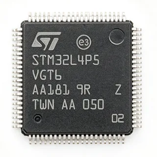
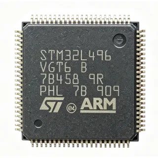
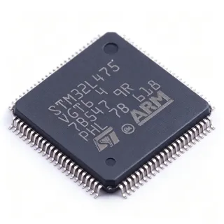
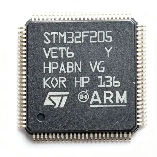
STM32F411VET6TR - 100MHz Cortex-M4 MCU 512KB Flash | STMicroelectronics
料号: STM32F411VET6TR ✓ 量产中| 数量 | 单价 | 小计 |
|---|---|---|
| 1 | $8.92 | $8.92 |
| 10 | $7.85 | $78.50 |
| 100 | $6.74 | $674.00 |
| 500 | $5.99 | $2,995.00 |
| 1,000 | $5.42 | $5,420.00 |
STM32F411VET6TR 概述
A microcontroller (MCU) is a single-chip computer that integrates a CPU core, program memory (Flash), working memory (SRAM), and a rich set of peripherals such as timers, ADCs, communication controllers, and GPIOs. The STM32F411 sits in the Cortex-M4 -> ARM Cortex-M family -> 32-bit RISC microcontroller hierarchy, designed for deterministic real-time control with hardware floating-point acceleration and DSP extensions, which makes it well suited to motor control, audio processing, and signal-chain conditioning where 8/16-bit MCUs lack the headroom.
Key features of the STM32F411VET6TR include 125 DMIPS / 273 CoreMark performance, an ART Accelerator with 8 KB instruction cache that delivers near-zero-wait-state execution from Flash, a USB 2.0 OTG Full-Speed controller with on-chip PHY, and an SDMMC interface. The analog subsystem integrates three 12-bit 2.4 MSPS ADCs, two 12-bit DACs, and a buffered reference. Communication peripherals cover up to three USART, two UART, three SPI, two I2C, one CAN 2.0B, plus an external memory bus for SRAM/NOR/NAND. The 100-LQFP package exposes 81 GPIO for flexible system integration.
Architecturally, the STM32F411 uses a multi-AHB bus matrix (DCODE, SYSTEM, DMA1, DMA2) with two seven-channel DMAs to keep peripheral and CPU traffic parallelized, and a Cortex-M4 core with single-precision FPU, MPU, and NVIC for hardware-prioritized interrupts. Power gating through the integrated PVD, low-power Run, Sleep, Stop, and Standby modes is coordinated by the RCC and PWR blocks to support battery-powered end products.
Typical applications include USB HID/CDC devices, sensor fusion nodes, audio front ends (USB microphone, USB headphone), digital power conversion, drones, gaming controllers, and human-machine interface (HMI) modules. The 100 MHz Cortex-M4 with hardware FPU also makes it a frequent choice for CNC pre-processors and industrial gateways requiring deterministic wired connectivity.
When designing with this device, route the VDD/VDDA pins through a star topology with separate 100 nF + 4.7 uF decoupling at each pin, and tie BOOT0 to ground via 10 kOhm for normal boot from Flash. The 100-LQFP requires thermal relief and proper copper pour for the 81 GPIO to keep switching noise out of the analog domain.
This page synthesizes distributor pricing, drop-in alternatives in the same 100-LQFP footprint, and practical design notes not found in the manufacturer datasheet.
直接替换替代料: STM32F411VET6TR ——相同封装,引脚兼容。需要 PCB 改动的不同封装料号已排除。
本系列中的变体
可与以下型号直接替换的同系列型号: STM32F411VET6TR (相同外形与封装尺寸) ——差异在于 Package, Communication Interfaces, Operating Temperature, ADC, Core.
快速对比工具——选择替代料号进行并排对比:
STM32F411VET6
✅ 直接替换✓ 有现货
联系询价
查看数据手册 →STM32F411RET6TR
✅ 直接替换✓ 有现货
$4.02 / 个
查看数据手册 →STM32F405VGT6TR
✅ 直接替换✓ 有现货
$8.1 / 个
查看数据手册 →STM32F407VET6TR
✅ 直接替换✓ 有现货
$3.4498 / 个
查看数据手册 →GD32F303VET6
✅ 直接替换📋 参考替代料(不在目录中)
STM32F411VET6TR 最大额定值与电气特性
| Core Architecture | ARM Cortex-M4 with FPU and DSP |
| 最大时钟频率 | 100 MHz |
| Performance | 125 DMIPS / 273 CoreMark |
| Program Memory (Flash) | 512 KB |
| SRAM | 128 KB |
| Supply Voltage (VDD) | 1.7 V to 3.6 V |
| 工作温度 | -40 C to +85 C (grade 6) |
| 封装 | 100-LQFP (14x14 mm) |
| GPIO Count | 81 |
| ADC | 3x 12-bit, 2.4 MSPS |
| DAC | 2x 12-bit |
| USB | USB 2.0 OTG Full-Speed with on-chip PHY |
| CAN | 1x CAN 2.0B |
| SDMMC | Yes |
| External Memory Bus | Yes (SRAM/NOR/NAND) |
| DMA | 2x 7-channel controllers |
| ART Accelerator | 8 KB instruction cache |
| 安装类型 | Surface Mount |
| RoHS 状态 | Compliant |
STM32F411VET6TR 引脚配置
| 引脚 1 | PE2 — GPIO PE2 / TRACECLK / FSMC_A23 |
| 引脚 2 | PE3 — GPIO PE3 / TRACED0 / FSMC_A19 |
| 引脚 3 | PE4 — GPIO PE4 / TRACED1 / FSMC_A20 |
| 引脚 4 | PE5 — GPIO PE5 / TRACED2 / FSMC_A21 |
| 引脚 5 | PE6 — GPIO PE6 / TRACED3 / FSMC_A22 |
| 引脚 6 | VBAT — Backup battery supply input |
| 引脚 7 | PC13 — GPIO PC13 / RTC_TAMP1 / WKUP2 |
| 引脚 8 | PC14 — GPIO PC14 / OSC32_IN |
| 引脚 9 | PC15 — GPIO PC15 / OSC32_OUT |
| 引脚 10 | VSS — Ground |
| 引脚 11 | VDD — Digital supply 1.7-3.6 V |
| 引脚 12 | OSC_IN — HSE oscillator input |
| 引脚 13 | OSC_OUT — HSE oscillator output |
| 引脚 14 | NRST — Active-low reset input |
| 引脚 15 | PC0 — GPIO PC0 / ADC1_IN10 |
| 引脚 16 | PC1 — GPIO PC1 / ADC1_IN11 |
| 引脚 17 | PC2 — GPIO PC2 / ADC1_IN12 |
| 引脚 18 | PC3 — GPIO PC3 / ADC1_IN13 |
| 引脚 19 | VSSA — Analog ground |
| 引脚 20 | VDDA — Analog supply 1.7-3.6 V |
| 引脚 21 | PA0 — GPIO PA0 / WKUP / ADC1_IN0 / TIM2_CH1 |
| 引脚 22 | PA1 — GPIO PA1 / ADC1_IN1 / TIM2_CH2 |
| 引脚 23 | PA2 — GPIO PA2 / USART2_TX / ADC1_IN2 / TIM2_CH3 |
| 引脚 24 | PA3 — GPIO PA3 / USART2_RX / ADC1_IN3 / TIM2_CH4 |
| 引脚 25 | VSS — Ground |
| 引脚 26 | VDD — Digital supply 1.7-3.6 V |
| 引脚 27 | PA4 — GPIO PA4 / SPI1_NSS / ADC1_IN4 / DAC1_OUT |
| 引脚 28 | PA5 — GPIO PA5 / SPI1_SCK / ADC1_IN5 / DAC2_OUT |
| 引脚 29 | PA6 — GPIO PA6 / SPI1_MISO / ADC1_IN6 / TIM3_CH1 |
| 引脚 30 | PA7 — GPIO PA7 / SPI1_MOSI / ADC1_IN7 / TIM3_CH2 |
| 引脚 31 | PC4 — GPIO PC4 / ADC1_IN14 |
| 引脚 32 | PC5 — GPIO PC5 / ADC1_IN15 |
| 引脚 33 | PB0 — GPIO PB0 / ADC1_IN8 / TIM3_CH3 |
| 引脚 34 | PB1 — GPIO PB1 / ADC1_IN9 / TIM3_CH4 |
| 引脚 35 | PB2 — GPIO PB2 / BOOT1 |
| 引脚 36 | PE7 — GPIO PE7 / FSMC_D4 |
| 引脚 37 | PE8 — GPIO PE8 / FSMC_D5 |
| 引脚 38 | PE9 — GPIO PE9 / FSMC_D6 |
| 引脚 39 | PE10 — GPIO PE10 / FSMC_D7 |
| 引脚 40 | PE11 — GPIO PE11 / FSMC_D8 |
| 引脚 41 | PE12 — GPIO PE12 / FSMC_D9 |
| 引脚 42 | PE13 — GPIO PE13 / FSMC_D10 |
| 引脚 43 | PE14 — GPIO PE14 / FSMC_D11 |
| 引脚 44 | PE15 — GPIO PE15 / FSMC_D12 |
| 引脚 45 | PB10 — GPIO PB10 / I2C2_SCL / USART3_TX |
| 引脚 46 | PB11 — GPIO PB11 / I2C2_SDA / USART3_RX |
| 引脚 47 | VCAP_1 — Core voltage decoupling (1.2 V LDO output) |
| 引脚 48 | VDD — Digital supply 1.7-3.6 V |
| 引脚 49 | PB12 — GPIO PB12 / SPI2_NSS / I2S2_WS |
| 引脚 50 | PB13 — GPIO PB13 / SPI2_SCK / I2S2_CK |
| 引脚 51 | PB14 — GPIO PB14 / SPI2_MISO / TIM12_CH1 |
| 引脚 52 | PB15 — GPIO PB15 / SPI2_MOSI / TIM12_CH2 |
| 引脚 53 | PD8 — GPIO PD8 / FSMC_D13 / USART3_TX |
| 引脚 54 | PD9 — GPIO PD9 / FSMC_D14 / USART3_RX |
| 引脚 55 | PD10 — GPIO PD10 / FSMC_D15 |
| 引脚 56 | PD11 — GPIO PD11 / FSMC_A16 |
| 引脚 57 | PD12 — GPIO PD12 / FSMC_A17 / TIM4_CH1 |
| 引脚 58 | PD13 — GPIO PD13 / FSMC_A18 / TIM4_CH2 |
| 引脚 59 | PD14 — GPIO PD14 / FSMC_D0 / TIM4_CH3 |
| 引脚 60 | PD15 — GPIO PD15 / FSMC_D1 / TIM4_CH4 |
| 引脚 61 | PC6 — GPIO PC6 / USART6_TX / TIM3_CH1 |
| 引脚 62 | PC7 — GPIO PC7 / USART6_RX / TIM3_CH2 |
| 引脚 63 | PC8 — GPIO PC8 / SDMMC_D0 / TIM3_CH3 |
| 引脚 64 | PC9 — GPIO PC9 / SDMMC_D1 / TIM3_CH4 |
| 引脚 65 | PA8 — GPIO PA8 / USART1_CK / TIM1_CH1 / MCO1 |
| 引脚 66 | PA9 — GPIO PA9 / USART1_TX / TIM1_CH2 |
| 引脚 67 | PA10 — GPIO PA10 / USART1_RX / TIM1_CH3 |
| 引脚 68 | PA11 — GPIO PA11 / USB_DM / CAN1_RX |
| 引脚 69 | PA12 — GPIO PA12 / USB_DP / CAN1_TX |
| 引脚 70 | PA13 — GPIO PA13 / JTMS / SWDIO |
| 引脚 71 | VCAP_2 — Core voltage decoupling (1.2 V LDO output) |
| 引脚 72 | VDD — Digital supply 1.7-3.6 V |
| 引脚 73 | PA14 — GPIO PA14 / JTCK / SWDCLK |
| 引脚 74 | PA15 — GPIO PA15 / JTDI / SPI1_NSS / TIM2_CH1 |
| 引脚 75 | PC10 — GPIO PC10 / SDMMC_D2 / USART3_TX |
| 引脚 76 | PC11 — GPIO PC11 / SDMMC_D3 / USART3_RX |
| 引脚 77 | PC12 — GPIO PC12 / SDMMC_CK / USART3_CK |
| 引脚 78 | PD0 — GPIO PD0 / FSMC_D2 / CAN1_RX |
| 引脚 79 | PD1 — GPIO PD1 / FSMC_D3 / CAN1_TX |
| 引脚 80 | PD2 — GPIO PD2 / SDMMC_CMD / TIM3_ETR |
| 引脚 81 | PD3 — GPIO PD3 / FSMC_CLK / USART2_CTS |
| 引脚 82 | PD4 — GPIO PD4 / FSMC_NOE / USART2_RTS |
| 引脚 83 | PD5 — GPIO PD5 / FSMC_NWE / USART2_TX |
| 引脚 84 | PD6 — GPIO PD6 / FSMC_NWAIT / USART2_RX |
| 引脚 85 | PD7 — GPIO PD7 / FSMC_NE1 / USART2_CK |
| 引脚 86 | PB3 — GPIO PB3 / JTDO / TRACESWO / SPI1_SCK / TIM2_CH2 |
| 引脚 87 | PB4 — GPIO PB4 / NJTRST / SPI1_MISO / TIM3_CH1 |
| 引脚 88 | PB5 — GPIO PB5 / SPI1_MOSI / I2C1_SMBA / TIM3_CH2 |
| 引脚 89 | PB6 — GPIO PB6 / I2C1_SCL / USART1_TX / TIM4_CH1 |
| 引脚 90 | PB7 — GPIO PB7 / I2C1_SDA / USART1_RX / TIM4_CH2 |
| 引脚 91 | BOOT0 — Boot mode select (0 = main Flash, 1 = system bootloader) |
| 引脚 92 | PB8 — GPIO PB8 / I2C1_SCL / CAN1_RX / TIM4_CH3 |
| 引脚 93 | PB9 — GPIO PB9 / I2C1_SDA / CAN1_TX / TIM4_CH4 |
| 引脚 94 | PE0 — GPIO PE0 / TIM4_ETR |
| 引脚 95 | PE1 — GPIO PE1 / FSMC_NBL0 |
| 引脚 96 | VSS — Ground |
| 引脚 97 | VSS — Ground |
| 引脚 98 | PE2_ALT — Alias region for PE2 / FSMC_A23 (per datasheet) |
| 引脚 99 | VREF+ — ADC/DAC positive reference voltage |
| 引脚 100 | VREF- — ADC/DAC negative reference voltage |
典型应用
STM32F411VET6TR 适用于 6 应用s: USB HID / CDC Device, Sensor Fusion / IMU Node, Audio Front End (USB Microphone / Headset), Industrial Gateway / HMI Controller, Drone Flight Controller Companion Board, Gaming Controller / HMI Bridge.
USB HID / CDC Device
The STM32F411VET6TR is a strong fit for USB Human Interface Devices and CDC virtual COM ports because of its integrated USB 2.0 OTG Full-Speed controller with on-chip PHY, removing the need for an external transceiver. The 100 MHz Cortex-M4 with hardware FPU handles USB stack processing, HID report packing, and CDC line coding within budget, while 512 KB Flash fits full USB class stacks (HID + CDC composite) plus a small RTOS. Use it for configuration tools, lab instruments, and custom peripherals where a 12 Mbps USB link and PC driverless enumeration are required. Power dissipation is modest at 100 MHz full load, so no external heatsinking is needed on the 100-LQFP.
推荐
Sensor Fusion / IMU Node
The STM32F411VET6TR suits 9-axis IMU sensor fusion nodes because its 100 MHz Cortex-M4 with FPU and DSP can run a real-time Madgwick or Mahony filter with 1 kHz update rates. The 3x 12-bit 2.4 MSPS ADCs sample analog sensor outputs while the SPI and I2C controllers drive the accelerometer, gyro, and magnetometer, and the DMA offloads conversion to memory without CPU intervention. The 128 KB SRAM accommodates FIFO buffers and the filter state, while 512 KB Flash holds the bootloader, RTOS, and sensor drivers. 1.7-3.6 V operation is friendly to Li-ion battery rails commonly used in wearables and drones.
推荐
Audio Front End (USB Microphone / Headset)
The STM32F411VET6TR is a common choice for USB audio peripherals because the USB OTG Full-Speed link can stream 48 kHz / 16-bit stereo audio over isochronous endpoints while the Cortex-M4 performs basic DSP, gain control, and sidetone. The 2x 12-bit DAC and I2S interface support headphone or line-out stages, and the SDMMC controller enables optional WAV file playback from a microSD card. With 128 KB SRAM the MCU can buffer several milliseconds of audio while leaving headroom for the USB stack, and 512 KB Flash holds a full USB audio class 1.0 implementation. Power is held low enough for bus-powered designs drawing 100 mA or less from USB.
推荐
Industrial Gateway / HMI Controller
The STM32F411VET6TR fits industrial gateway and HMI controller roles where deterministic RS-485, Modbus, or CAN 2.0B communication and a TFT display are required. The 100-LQFP exposes 81 GPIO, three USART, two UART, three SPI, two I2C, and a CAN 2.0B interface, supporting multi-drop industrial networks and parallel LCD/SDRAM through the external memory bus. The Cortex-M4 with FPU handles protocol stacks plus a small LVGL or emWin HMI, and 512 KB Flash comfortably stores bootloader, application, OTA staging, and fonts. -40 to +85 C operation and 3.6 V tolerant I/O are aligned with industrial cabinet environments.
推荐
Drone Flight Controller Companion Board
The STM32F411VET6TR works well as a companion processor or payload controller in drone systems, offloading navigation, camera control, or telemetry from the main flight controller. The 100 MHz Cortex-M4 with FPU executes CMSIS-DSP and CMSIS-NN inferences for on-board computer vision, while the SDMMC interface logs mission data to microSD. CAN and USART provide robust links to ESCs and the flight controller, and the 81 GPIO drive auxiliary actuators. Battery-friendly 1.7-3.6 V operation supports direct Li-Po input through a small LDO, and the small 100-LQFP footprint fits tight companion boards.
推荐
Gaming Controller / HMI Bridge
The STM32F411VET6TR can serve as the bridge MCU in wired and wireless gaming controllers, scanning button matrices, driving RGB LED chains, and presenting a USB HID or Bluetooth-HID endpoint. The 100 MHz Cortex-M4 with FPU runs USB-HID class driver plus anti-aliasing filtering on analog sticks, and the timers drive PWM for rumble motors with hardware dead-time insertion. 128 KB SRAM holds debounced input FIFOs and a USB report buffer, while 512 KB Flash carries bootloader, application, and device profiles. 1.7-3.6 V operation supports direct Li-ion battery power with simple boost regulation.
推荐
推荐产品汇总
工程参考数据: STM32F411VET6TR ——对比、设计指导和合规信息。
选型指南
与替代料对比
| 参数 | 本产品 | STM32F411VET6 | STM32F411RET6TR | STM32F405VGT6TR | STM32F407VET6TR | GD32F303VET6 |
|---|---|---|---|---|---|---|
| Brand | STMicroelectronics | STMicroelectronics | STMicroelectronics | STMicroelectronics | STMicroelectronics | GigaDevice |
| Package | 100-LQFP (14x14) | 100-LQFP (14x14) - same | 100-LQFP (14x14) - same | 100-LQFP (14x14) - same | 100-LQFP (14x14) - same | 100-LQFP (14x14) - same |
| Core | Cortex-M4F @ 100 MHz | Cortex-M4F @ 100 MHz | Cortex-M4F @ 100 MHz | Cortex-M4F @ 168 MHz | Cortex-M4F @ 168 MHz | Cortex-M4 (no FPU) @ 120 MHz |
| Flash | 512 KB | 512 KB | 256 KB | 1 MB | 512 KB | 512 KB |
| SRAM | 128 KB | 128 KB | 128 KB | 192 KB | 128 KB | 64 KB |
| USB | USB OTG FS, on-chip PHY | USB OTG FS, on-chip PHY | USB OTG FS, on-chip PHY | USB OTG FS + HS (ext PHY) | USB OTG FS + HS (ext PHY) | USB OTG FS |
| Ethernet MAC | No | No | No | Yes (MII/RMII) | Yes (MII/RMII) | No |
| FPU | Yes (single-precision) | Yes | Yes | Yes | Yes | No |
关键差异点
- Higher performance than STM32F411RET6 with same 100-LQFP footprint (对比 STM32F411RET6TR)
- USB OTG Full-Speed with on-chip PHY, no external transceiver required (对比 STM32F405VGT6TR)
- GigaDevice cross-source option for cost reduction (对比 GD32F303VET6)
设计说明
Estimated: at 100 MHz full CPU load and 3.3 V VDD, the typical core current of an STM32F411 is around 12-15 mA. Add at least 100 nF + 4.7 uF ceramic on every VDD pin (48, 72, 11, 25, 26) plus 100 nF + 1 uF on VDDA pin 20, routed with star topology. Place a ferrite bead on the analog supply if the ADC is used at better than 10-bit effective resolution. Tie BOOT0 low through 10 kOhm to ground for normal Flash boot.
Estimated: at maximum 100 MHz and 3.6 V with all peripherals active, the package dissipation is well under 200 mW and the 100-LQFP with 1 oz 4-layer copper does not require a heatsink. Keep the exposed center pad in mind when migrating to a different STM32F4 with exposed pad (LQFP64/100 has no center pad; LQFP176/176BGA do). For industrial -40 to +85 C operation, derate clock speed above 70 C ambient if the application drives many GPIOs at high slew.
Do not leave NRST floating - it must have an external 10 kOhm pull-up and a 100 nF cap to ground for clean reset. The OSC_IN/OSC_OUT pins require a load-capacitor pair sized to the crystal (typically 5-20 pF). PC13 through PC15 on the 100-LQFP are shared with the RTC domain - do not use them as outputs if the RTC tamper or wake-up function is needed. BOOT0 must be sampled at NRST deassertion; if you reconfigure BOOT0 in firmware, it has no effect until the next reset.
合规信息
Industrial grade-6 -40 to +85 C; not AEC-Q100 qualified - use STM32F4 automotive grades (e.g. STM32F412RG) for automotive designs