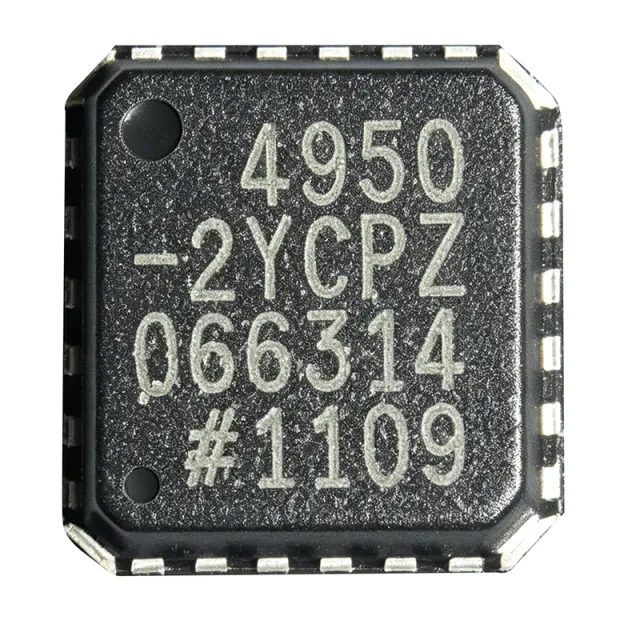
ADA4950-2YCPZ - Dual Differential ADC Driver | Analog Devices
MPN: ADA4950-2YCPZ ✓ نشط| الكمية | سعر الوحدة | الإجمالي |
|---|---|---|
| 1 | $8.58 | $8.58 |
| 10 | $7.72 | $77.20 |
| 100 | $6.23 | $623.00 |
| 500 | $5.5 | $2,750.00 |
| 1,000 | $4.95 | $4,950.00 |
ADA4950-2YCPZ نظرة عامة
A differential amplifier is an electronic amplifier that amplifies the difference between two input voltages while rejecting common-mode signals. In the context of ADC driving, a differential amplifier converts a single-ended signal to a differential signal or buffers a differential signal, providing the necessary drive strength and level shifting to interface with high-performance analog-to-digital converters. The ADA4950-2 is specifically optimized for this role, offering low noise, low distortion, and high bandwidth to preserve signal integrity.
Key features of the ADA4950-2 include a -3 dB bandwidth of 1.35 GHz (gain = 1), a slew rate of 2900 V/µs, and a low input voltage noise of 2.2 nV/√Hz. The device provides a differential output with a common-mode voltage set by an internal reference, simplifying interface to ADCs. It also features a power-down mode to conserve energy when not in use. The on-chip gain resistors eliminate the need for external resistor networks, reducing board space and component count.
The ADA4950-2 is well-suited for a wide range of applications, including communications, instrumentation, and medical imaging. Its high bandwidth and low distortion make it ideal for driving high-speed ADCs in software-defined radios, radar systems, and test equipment. The low power consumption (typically 9.5 mA per amplifier) is beneficial for portable and battery-powered devices.
When designing with the ADA4950-2, it is important to consider proper power supply decoupling and PCB layout to achieve optimal performance. The exposed pad on the LFCSP package should be soldered to a ground plane for thermal and electrical performance. Additionally, the input common-mode voltage range and output swing should be checked against the ADC's input requirements to ensure proper operation.
بدائل مباشرة لـ ADA4950-2YCPZ — نفس الحزمة، متوافق دبوس بدبوس. تُستثنى القطع ذات الحزم المختلفة التي تتطلب تعديل PCB.
أداة المقارنة السريعة — اختر قطعًا بديلة للمقارنة جنبًا إلى جنب:
ADA4950-2YCPZ-RL7
تواصل لمعرفة السعر
عرض ورقة البيانات ←ADA4950-2YCPZ-R7
📋 بديل مرجعي (غير موجود في الكتالوج)
ADA4950-2YCPZ-R2
📋 بديل مرجعي (غير موجود في الكتالوج)
ADA4932-2YCPZ
📋 بديل مرجعي (غير موجود في الكتالوج)
ADA4930-2YCPZ
📋 بديل مرجعي (غير موجود في الكتالوج)
THS4509
📋 بديل مرجعي (غير موجود في الكتالوج)
ADA4950-2YCPZ الحدود القصوى والخصائص الكهربائية
| Number of Channels | 2 (Dual) |
| Gain Options | 1, 2, 3 (fixed, on-chip) |
| Supply Voltage Range (Single) | 3.3 V to 11 V |
| Supply Voltage Range (Dual) | ±1.65 V to ±5.5 V |
| Bandwidth (-3 dB) | 1.35 GHz (G = 1) |
| Slew Rate | 2900 V/µs |
| Input Voltage Noise | 2.2 nV/√Hz |
| Input Offset Voltage | 0.5 mV (typical) |
| Input Bias Current | 2 µA (typical) |
| Output Current | 60 mA (typical) |
| Supply Current (per amplifier) | 9.5 mA (typical) |
| Power-Down Current | 0.3 mA (typical) |
| نطاق درجة حرارة التشغيل | -40°C to +105°C |
| العلبة | 24-Lead LFCSP (4x4 mm) |
| نوع التركيب | Surface Mount |
| حالة RoHS | Compliant |
تكوين أطراف ADA4950-2YCPZ
| دبوس 1 | OUT+ — Positive differential output |
| دبوس 2 | OUT- — Negative differential output |
| دبوس 3 | VOCM — Output common-mode voltage set |
| دبوس 4 | GND — Ground |
| دبوس 5 | IN+ — Non-inverting input |
| دبوس 6 | IN- — Inverting input |
| دبوس 7 | V+ — Positive supply |
| دبوس 8 | V- — Negative supply (or ground for single supply) |
| دبوس 9 | PD — Power-down (active high) |
| دبوس 10 | G1 — Gain select 1 |
| دبوس 11 | G0 — Gain select 0 |
| دبوس 12 | NC — No connect |
التطبيقات النموذجية
ADA4950-2YCPZ مناسب لـ 6 التطبيقs: High-Speed ADC Driver, Software-Defined Radio, Medical Imaging, Test and Measurement, Communications Infrastructure, Radar Systems.
High-Speed ADC Driver
The ADA4950-2YCPZ is ideal for driving high-speed ADCs in communications and instrumentation. Its 1.35 GHz bandwidth and low distortion ensure that the ADC input signal is faithfully reproduced. The fixed gain options simplify the interface, and the low noise (2.2 nV/√Hz) preserves signal-to-noise ratio. The differential output directly connects to ADC inputs, reducing common-mode noise. Power consumption of 9.5 mA per amplifier is suitable for multi-channel systems.
موصى به
Software-Defined Radio
In software-defined radios, the ADA4950-2YCPZ drives the ADC that digitizes the IF signal. Its high bandwidth and low distortion are critical for preserving signal integrity in wideband receivers. The gain-selectable feature allows optimization for different signal levels. The low power consumption is beneficial for portable SDR platforms. The differential output reduces common-mode interference, improving receiver sensitivity.
موصى به
Medical Imaging
The ADA4950-2YCPZ is used in medical imaging systems such as ultrasound and MRI, where high-speed ADC drivers are required. Its low noise and low distortion ensure accurate signal acquisition. The small LFCSP package is suitable for compact imaging probes. The wide supply voltage range allows operation from various power rails. The power-down mode helps reduce power consumption when not imaging.
موصى به
Test and Measurement
In test and measurement equipment, the ADA4950-2YCPZ drives ADCs in oscilloscopes, spectrum analyzers, and signal generators. Its high bandwidth and fast slew rate (2900 V/µs) handle high-frequency signals with minimal distortion. The fixed gain options simplify calibration. The low noise ensures accurate measurements. The device's robustness over -40°C to +105°C makes it suitable for benchtop and field instruments.
موصى به
Communications Infrastructure
The ADA4950-2YCPZ is used in base stations and communication systems to drive ADCs in receivers. Its high linearity and low distortion are essential for handling multiple carriers. The differential output reduces common-mode noise, improving receiver performance. The low power consumption is important for high-density channel cards. The gain-selectable feature allows adaptation to different signal levels.
موصى به
Radar Systems
In radar systems, the ADA4950-2YCPZ drives ADCs that digitize the received signal. Its high bandwidth and fast slew rate are critical for capturing short pulses. The low noise improves detection sensitivity. The wide supply voltage range allows operation from various power rails. The small package is suitable for phased-array modules. The power-down mode helps manage thermal load.
موصى به
ملخص المنتجات الموصى بها
بيانات مرجعية هندسية لـ ADA4950-2YCPZ — المقارنة وإرشادات التصميم ومعلومات الامتثال.
دليل الاختيار
المقارنة مع البدائل
| المعامل | هذا المنتج | ADA4950-2YCPZ-RL | ADA4950-2YCPZ-R7 | ADA4932-2YCPZ | ADA4930-2YCPZ | THS4509 |
|---|---|---|---|---|---|---|
| Package | 24-Lead LFCSP (4x4 mm) | 24-Lead LFCSP (4x4 mm) | 24-Lead LFCSP (4x4 mm) | 24-Lead LFCSP (4x4 mm) | 24-Lead LFCSP (4x4 mm) | 24-Lead LFCSP (4x4 mm) |
| Brand | Analog Devices | Analog Devices | Analog Devices | Analog Devices | Analog Devices | Texas Instruments |
| Number of Channels | 2 | 2 | 2 | 2 | 2 | 1 |
| Gain Options | 1, 2, 3 (fixed) | 1, 2, 3 (fixed) | 1, 2, 3 (fixed) | External resistors | 1, 2, 3 (fixed) | External resistors |
| Bandwidth (-3 dB) | 1.35 GHz | 1.35 GHz | 1.35 GHz | 1.35 GHz | 1.4 GHz | 1.9 GHz |
| Slew Rate | 2900 V/µs | 2900 V/µs | 2900 V/µs | 2900 V/µs | 2900 V/µs | 6600 V/µs |
| Input Voltage Noise | 2.2 nV/√Hz | 2.2 nV/√Hz | 2.2 nV/√Hz | 2.2 nV/√Hz | 2.2 nV/√Hz | 1.6 nV/√Hz |
| Supply Current (per amp) | 9.5 mA | 9.5 mA | 9.5 mA | 9.5 mA | 9.5 mA | 20 mA |
أبرز الفروقات
- On-chip gain resistors (مقابلADA4932-2YCPZ)
- Lower power consumption (مقابلTHS4509)
- Dual channel in small package (مقابلTHS4509)
ملاحظات التصميم
The ADA4950-2YCPZ operates from a single 3.3V to 11V supply or dual ±1.65V to ±5.5V supplies. Ensure that the supply voltage is within the specified range and that adequate decoupling capacitors (0.1 µF and 10 µF) are placed close to the V+ and V- pins. The power-down pin (PD) can be used to reduce current consumption to 0.3 mA when the amplifier is not in use.
For optimal performance, place the ADA4950-2YCPZ close to the ADC it drives. Use a solid ground plane and minimize trace lengths for the differential output. The exposed pad on the LFCSP package should be soldered to the ground plane to improve thermal performance and reduce parasitic inductance. Follow the layout guidelines in the datasheet for best results.
Ensure that the input common-mode voltage is within the specified range to avoid clipping. The output common-mode voltage is set by the VOCM pin; connect it to the ADC's reference voltage for proper level shifting. Do not leave the gain select pins floating; tie them to V+ or GND to set the desired gain. Verify that the power-down pin is not accidentally asserted.
معلومات الامتثال
RoHS compliant per Analog Devices product page. Not AEC-Q100 qualified. Lead-free per datasheet.






