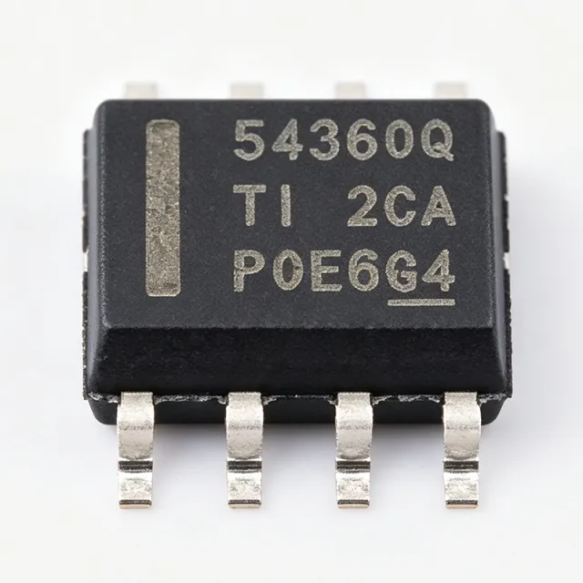
TPS54360QDDARQ1 - 60V 3.5A Buck Converter | Texas Instruments
MPN: TPS54360QDDARQ1 ✓ نشطTPS54360QDDARQ1 نظرة عامة
A buck (step-down) converter is a switching voltage regulator that converts a higher input voltage to a lower regulated output using an internal power switch, external inductor, and output capacitor. Within the power management hierarchy, this device sits in the DC-DC converter family, part of the broader voltage regulator and power management IC (PMIC) domain, optimized for wide-input point-of-load conversion directly from automotive battery rails.
Key features include a 60V maximum input with 65V transient survivability per ISO 7637 load-dump testing, 3.5A continuous output current, TI Eco-mode pulse-skip operation for high light-load efficiency, and current-mode control for simple external compensation and flexible component selection. The automotive Q1 qualification and -40C to +125C ambient range enable deployment in harsh vehicle environments.
Architecturally, the device uses peak current-mode control with an integrated 60V power MOSFET, reducing external component count versus a controller-plus-discrete-FET solution. The low-ripple pulse-skip Eco-mode reduces switching losses at light loads, while the internal bootstrap and soft-start functions simplify startup design. The SO-8 PowerPAD exposed pad provides a low thermal resistance path for heat dissipation.
Typical applications include automotive infotainment and cluster power rails, 12V/24V industrial bus point-of-load conversion, USB and display bias supplies, and general-purpose wide-input regulation from 24V industrial systems.
Design consideration: at 60V input the converter operates at high switching-step ratios; ensure the external inductor saturation current exceeds the 3.5A peak limit and follow the TI datasheet layout guidelines, placing the input decoupling capacitor very close to VIN and GND pins.
بدائل مباشرة لـ TPS54360QDDARQ1 — نفس الحزمة، متوافق دبوس بدبوس. تُستثنى القطع ذات الحزم المختلفة التي تتطلب تعديل PCB.
الطرازات في هذه السلسلة
طرازات من نفس السلسلة متوافقة تمامًا مع TPS54360QDDARQ1 (نفس عامل الشكل والبصمة) — يختلف في Output Voltage Range, Package, Input Voltage Range, Topology, Maximum Output Current.
TPS54360DDAR
تواصل لمعرفة السعر
عرض ورقة البيانات ←TPS5450QDDARQ1
تواصل لمعرفة السعر
عرض ورقة البيانات ←TPS5430QDDARQ1
تواصل لمعرفة السعر
عرض ورقة البيانات ←TPS54360BQDDARQ1
📋 بديل مرجعي (غير موجود في الكتالوج)
TPS54560QDDARQ1
📋 بديل مرجعي (غير موجود في الكتالوج)
TPS54360QDDARQ1 الحدود القصوى والخصائص الكهربائية
| البنية الطوبولوجية | Buck (Step-Down) |
| نطاق جهد الدخل | 4.5 V to 60 V |
| نطاق جهد الخرج | 0.8 V adjustable upward |
| أقصى تيار خرج | 3.5 A |
| عدد المخارج | 1 |
| Load Dump Survivability | 65 V per ISO 7637 |
| Control Topology | Current Mode |
| Light-Load Mode | Eco-mode pulse-skip (low ripple) |
| درجة حرارة التشغيل | -40C to +125C |
| العلبة | 8-PowerSOIC (DDA, SO-8 PowerPAD, 3.90mm width) |
| نوع التركيب | Surface Mount |
| Qualification | AEC-Q100 (Automotive Q1) |
| Integrated FET | High-side MOSFET integrated |
تكوين أطراف TPS54360QDDARQ1
| دبوس 1 | BOOT — Bootstrap capacitor connection for high-side gate driver |
| دبوس 2 | VIN — Input supply, 4.5V to 60V |
| دبوس 3 | EN/UVLO — Enable and adjustable undervoltage lockout |
| دبوس 4 | SS/TR — Soft-start / tracking control |
| دبوس 5 | VSENSE — Feedback voltage sense for output regulation |
| دبوس 6 | COMP — Error amplifier output for loop compensation |
| دبوس 7 | GND — Ground reference |
| دبوس 8 | PH — Phase (switch node) connection to inductor |
| دبوس Pad | PowerPAD — Exposed thermal pad, must be soldered to grounded copper for thermal and electrical performance |
التطبيقات النموذجية
TPS54360QDDARQ1 مناسب لـ 6 التطبيقs: Automotive Battery-Direct Power Rails, 24V Industrial Bus Point-of-Load Conversion, Automotive Infotainment and Cluster Supplies, Motor Drive and Actuator Logic Supplies, Body Electronics and Lighting Modules, Telematics and Connectivity Modules.
Automotive Battery-Direct Power Rails
The TPS54360QDDARQ1 connects directly to 12V automotive battery rails because its 4.5V to 60V input range absorbs cold-crank down to 4.5V and load-dump transients up to 65V per ISO 7637 without external TVS sacrifice. Placed as the first-stage buck feeding downstream 5V or 3.3V point-of-load regulators, its integrated 60V high-side MOSFET and current-mode control deliver 3.5A with simple compensation. AEC-Q100 qualification and -40C to +125C rating remove the need for additional screening in automotive programs.
موصى به
24V Industrial Bus Point-of-Load Conversion
For 24V industrial control buses, the TPS54360QDDARQ1 provides headroom well above nominal rail levels while its Eco-mode pulse-skip maintains efficiency at light standby loads typical of always-on automation nodes. The 3.5A capability supports motor-control logic, sensor hubs, and communication modules. Current-mode control with external compensation lets engineers tune transient response to the load, and the SO-8 PowerPAD dissipates heat through a small PCB copper area, keeping the power stage compact inside DIN-rail and panel enclosures.
موصى به
Automotive Infotainment and Cluster Supplies
Infotainment head units and instrument clusters require clean, sequenced rails from battery input; the TPS54360QDDARQ1 serves as the primary wide-input buck generating a 5V intermediate rail from which audio amplifiers and display supplies derive power. Its 65V load-dump survivability protects the system during alternator transients, and its soft-start pin enables controlled power-up sequencing. With up to 3.5A continuous output, it directly powers display backlights and connectivity modules while Eco-mode limits idle drain when the vehicle is off.
موصى به
Motor Drive and Actuator Logic Supplies
Automotive and industrial motor drivers require robust local rails tolerant of inductive kickback and supply transients. The TPS54360QDDARQ1, with its 60V input and ISO 7637 pulse survivability, converts battery or 24V bus power into regulated logic rails for gate drivers and microcontrollers. Its current-mode architecture rejects input disturbance quickly, which matters when inductive loads cause bus droop. Pairing it with isolated gate drivers on the same board yields a complete compact motor-node power solution rated for harsh environments.
موصى به
Body Electronics and Lighting Modules
Body control modules, LED headlamp drivers, and lighting ECUs are wired directly to battery, facing load dump and jump-start events. The TPS54360QDDARQ1 delivers a regulated front-end for these modules, its Eco-mode cutting quiescent losses to protect battery state of charge. The -40C to +125C ambient range covers underhood and exterior lamp positions, and the AEC-Q1 qualification simplifies automotive customer approval. Its 3.5A output also directly feeds LED string regulation circuitry in mid-power lighting applications.
موصى به
Telematics and Connectivity Modules
Telematics units, gateways, and wireless modules must remain powered during engine crank where battery voltage dips toward 4.5V; the TPS54360QDDARQ1 maintains regulation across this window. With 3.5A available, it powers application processors and RF modules concurrently. The wide 60V tolerance also accommodates miswired or over-voltage input conditions common in field installations. Compact SO-8 PowerPAD packaging suits space-constrained telematics dongles, and Eco-mode reduces standby current for always-connected vehicle nodes.
موصى به
ملخص المنتجات الموصى بها
بيانات مرجعية هندسية لـ TPS54360QDDARQ1 — المقارنة وإرشادات التصميم ومعلومات الامتثال.
دليل الاختيار
المقارنة مع البدائل
| المعامل | هذا المنتج | TPS54360DDAR | TPS54360BQDDARQ1 | TPS54560QDDARQ1 | TPS5450QDDARQ1 | TPS5430QDDARQ1 |
|---|---|---|---|---|---|---|
| Package | SO-8 PowerPAD (DDA) | SO-8 PowerPAD (DDA) - same | SO-8 PowerPAD (DDA) - same | SO-8 PowerPAD (DDA) - same | SO-8 PowerPAD (DDA) - same | SO-8 PowerPAD (DDA) - same |
| Brand | Texas Instruments | Texas Instruments | Texas Instruments | Texas Instruments | Texas Instruments | Texas Instruments |
| Output Current | 3.5 A | 3.5 A | 3.5 A | 5 A | 5 A | 3 A |
| AEC-Q100 Qualification | Qualified (Q1) | Not qualified | Qualified (Q1) | Qualified (Q1) | Qualified (Q1) | Qualified (Q1) |
أبرز الفروقات
- Automotive AEC-Q1 qualification (مقابلTPS54360DDAR)
- Higher current headroom available in same footprint (مقابلTPS54560QDDARQ1)
- Superior input transient robustness (مقابلTPS5430QDDARQ1)
ملاحظات التصميم
The SO-8 PowerPAD exposed pad is the primary thermal path. Solder it to a grounded copper pour of at least 2x2 via-stitched area; without adequate PowerPAD connection the device cannot sustain 3.5A continuous output at elevated ambient temperatures. Follow the TI datasheet thermal design section when operating above ~2W dissipation.
Place the input decoupling capacitor as close as possible between VIN and GND to minimize high-frequency loop area, and keep the PH-to-inductor-to-output-capacitor loop compact. Use a solid ground plane referenced by the PowerPAD. Route the VSENSE feedback trace away from the PH switch node to avoid injecting switching noise into the error amplifier.
Select an inductor with saturation current above the 3.5A peak current limit, not merely the average load. Do not exceed 60V continuous input; although the device survives 65V ISO 7637 pulses, sustained over-voltage damages the integrated FET. Use the EN/UVLO divider to disable operation below safe battery levels during cold crank.
معلومات الامتثال
AEC-Q100 automotive qualification confirmed by Q1 suffix per TI product page. RoHS/REACH status to be confirmed on TI quality documentation.






