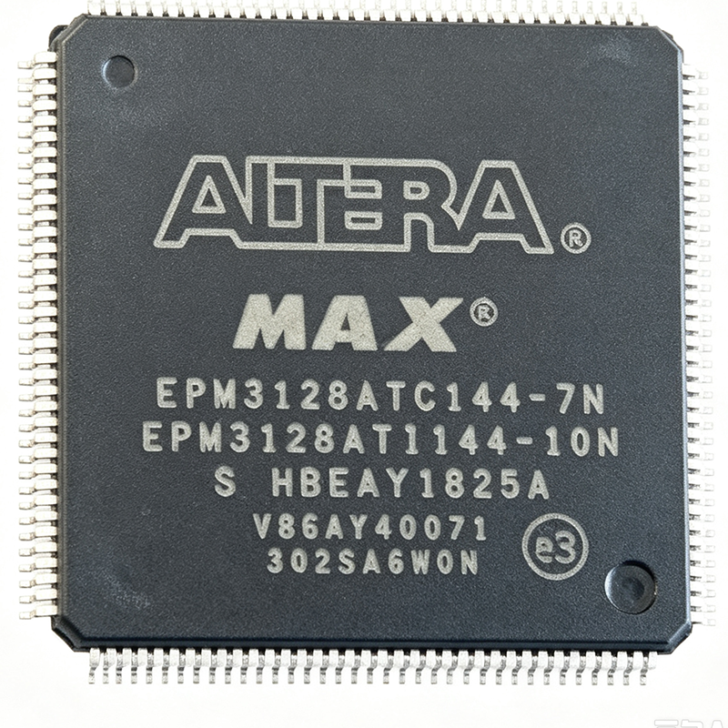
What Is the EPM3128ATC144-7N and Why Should Engineers Care?
The EPM3128ATC144-7N is an Altera (now Intel) MAX 3000A family CMOS EEPROM-based CPLD delivering 128 macrocells, up to 10,000 usable gates, 96 user I/Os, and a 7.5 ns pin-to-pin propagation delay in a 144-pin TQFP (20 x 20 mm, 0.5 mm pitch) package. Its 3.3 V core (VCCINT) pairs with MultiVolt I/O that accepts 2.5 V, 3.3 V, or 5.0 V supply (VCCIO), so one chip bridges 5 V legacy logic to modern 3.3 V and 2.5 V cores without external level shifters. The -7 speed grade supports counter frequencies up to 227.3 MHz and is compatible with the PCI Local Bus Specification, Revision 2.2 (PCI SIG). The -N suffix denotes a lead-free, RoHS-compliant finish. The part is currently listed as active on XAIPART with 99,999 units in stock, MOQ 1, and tiered pricing from $15.01 (qty 1) down to $9.25 (qty 1000) as of 2026-09-12.
Unlike SRAM-based FPGAs, the MAX 3000A stores its configuration in on-chip EEPROM, so it boots instantly with no external configuration memory and retains its bitstream for decades. That combination of instant-on operation, deterministic timing, high drive strength, and JTAG in-system programmability (IEEE 1149.1) makes it a workhorse for glue logic, bus interfaces, state machines, and power sequencing. This guide consolidates verified specifications, design-in practices, drop-in alternatives, and sourcing data so you can qualify the part in one place. For live stock and the full datasheet, see the EPM3128ATC144-7N product page on XAIPART.
How Do You Select and Design In the EPM3128ATC144-7N?
Confirm the Speed Grade Fits Your Timing Budget
The -7 suffix sets a 7.5 ns pin-to-pin propagation delay (tPD) and counter operation up to 227.3 MHz. If your system needs faster pin-to-pin paths, MAX 3000A speed grades run -4 (4.5 ns), -5 (5.0 ns), and -10 (10 ns). For PCI designs, note that speed grades -4 through -10 are compatible with the PCI Local Bus Specification, Revision 2.2, so the -7 grade meets PCI-SIG timing compliance while offering a balanced speed-versus-cost position.
Plan Your Power Architecture
Design the power tree around two supply domains. VCCINT requires 3.3 V for the core. VCCIO can be driven at 2.5 V, 3.3 V, or 5.0 V independently per I/O bank, which is what enables MultiVolt interfacing. In the TQFP-144 footprint, VCCINT pins appear at pins 42 and 137, and VCCIO pins at pins 77 and 106, per the verified pinout table. Decouple each supply pin close to the package; the 0.5 mm pitch TQFP-144 footprint with ground pouring also helps manage simultaneous-switching output (SSO) noise when many high-drive outputs switch together.
Map Your I/O Banks to Voltage Domains
The verified TQFP-144 pinout defines four I/O banks. Bank 1 occupies pins 1 through 36 and 138 through 144; Bank 2 covers pins 43 through 76; Bank 3 spans pins 78 through 105; Bank 4 covers pins 107 through 136. Group same-voltage signals within one bank, and reserve banks with 5.0 V VCCIO for legacy 5 V peripherals or PCI signaling while running other banks at 3.3 V or 2.5 V. The 96 user I/Os give you substantial headroom for address/data latching, chip selects, and status signals in one device.
Use JTAG for Programming and Field Updates
Dedicated JTAG pins sit at fixed locations: TDI on pin 37, TMS on pin 38, TCK on pin 39, and TDO on pin 40. The 3.3 V JTAG interface supports both in-system programming (ISP) of the EEPROM configuration and IEEE 1149.1 boundary-scan test, so you can program boards on the production line and push firmware updates in the field. Bring the four JTAG signals to a standard header even if you do not plan field updates; the cost is negligible and the flexibility is significant. Programmable security bits protect the design against unauthorized readback once programmed.
Stay Within the Commercial Temperature Range
The EPM3128ATC144-7N is rated 0 °C to +70 °C (commercial). For enclosures that can exceed that range, the industrial-grade EPM3128ATI144-7N covers -40 °C to +85 °C, per the MAX 3000A family offering referenced in the verified FAQ data. Do not derate the commercial part below 0 °C in the field; qualify the -I grade instead.
Budget Your Macrocells Realistically
The 128 macrocells are organized as 8 Logic Array Blocks of 16 macrocells each, connected through the programmable interconnect array (PIA). Verified application guidance suggests the following allocations: 32-48 macrocells for PCI address decoding plus 16-24 for cycle-state decoding; 16-24 macrocells for bus-arbitration state machines; 32-64 macrocells for a power-sequencing controller with watchdog; 32-48 macrocells for an 8x32 LED matrix refresh engine. Each macrocell supports sum-of-products with up to 36 inputs via the PIA, which lets single-macrocell wide decode functions replace dozens of 7400-series gates.
What Are the Best Drop-In Alternatives to the EPM3128ATC144-7N?
All MAX 3000A family members in the same TQFP-144 footprint with 128 macrocells and 96 user I/Os are pin-compatible drop-in options; only the speed grade and finish change. The verified FAQ data identifies three direct alternates. Choose by timing budget and compliance requirement, not by part number familiarity.
| Parameter | EPM3128ATC144-7N | EPM3128ATC144-7 | EPM3128ATC144-5N | EPM3128ATC144-10N |
|---|---|---|---|---|
| Propagation delay (tPD) | 7.5 ns | 7.5 ns | 5.0 ns | 10 ns |
| Macrocells | 128 | 128 | 128 | 128 |
| User I/Os | 96 | 96 | 96 | 96 |
| Package | TQFP-144 | TQFP-144 | TQFP-144 | TQFP-144 |
| Lead finish / RoHS | Pb-free (RoHS) | Tin-lead (SnPb), not RoHS | Pb-free (RoHS) | Pb-free (RoHS) |
| Drop-in on same footprint | Reference | Yes (identical silicon) | Yes (faster) | Yes (slower, lower cost) |
Selection logic, per the verified family guide: use the -7N when you need 7.5 ns timing and RoHS compliance; use the -5N when your timing budget tightens to 5.0 ns; use the -10N when 10 ns is acceptable and cost matters most; and treat the legacy SnPb -7 only as an option for grandfathered non-RoHS builds. Note that faster grades in a slower socket always work electrically, while a slower grade substituting for a faster one requires a full timing re-verification of every path. For current availability of any alternate, browse the XAIPART FPGA & CPLD category.
Where Is the EPM3128ATC144-7N in Its Lifecycle and How Should Buyers Source It?
The verified lifecycle status for the EPM3128ATC144-7N is active on the XAIPART platform, with 99,999 units in stock and MOQ 1 as of 2026-09-12. Verified FAQ sourcing data notes that the MAX 3000A family is being phased out by Intel/Altera and that distributor stock levels for legacy parts are declining, so real-time confirmation is essential before committing volume schedules. Verified distributor data points: Heisener listed 65,472 pieces in stock at $15.01 unit price with same-day shipping and 'Can Ship Immediately' status (estimated standard delivery Jul 15 - Jul 20 per the 2026-09-12 cached snapshot); authorized channels also include DigiKey (part number 544-1986-ND), Mouser, and Octopart aggregators.
Verified pricing as of 2026-09-12: $15.01 at qty 1, $13.50 at qty 10, $11.95 at qty 100, $10.40 at qty 500, and $9.25 at qty 1000. On a phased-out legacy line, obsolete-stock premiums can shift open-market pricing significantly, so lock tiered quotes in writing and consider scheduled deliveries from factory or franchised-distributor buffers. Buy only through authorized channels; counterfeit risk rises on legacy Intel/Altera parts transitioning out of production. [DATA_NEEDED: manufacturer last-time-order date and official discontinuation notice status]
What Trends Should Buyers and Designers Watch Around This CPLD?
Three trends anchored to verified specs should shape your decisions. First, the phase-out dynamic: active today (99,999 units on XAIPART as of 2026-09-12) does not mean available next quarter, so design new products only if you can accept a last-time-buy or a pin-compatible migration later. Second, the -7N's non-volatile EEPROM configuration and instant-on boot remain a genuine differentiator versus small SRAM FPGAs that need boot PROMs and load time; for glue logic, address decoding, bus arbitration, and power sequencing, a CPLD with deterministic 7.5 ns pin-to-pin timing and 10,000 usable gates is often the simpler, cheaper answer. Third, MultiVolt I/O (2.5 V/3.3 V/5.0 V) plus PCI Local Bus Rev. 2.2 compatibility keeps this part relevant in mixed-voltage industrial retrofit and legacy PCI maintenance designs where modern single-voltage logic cannot directly connect. When you evaluate successors, match these three capabilities explicitly: non-volatile instant-on configuration, deterministic sub-10 ns pin-to-pin delay, and 5 V-tolerant I/O banks. For replacement planning and cross-references, consult the XAIPART engineering blog and request lifecycle statements from your distributor.
Comments
Be the first to comment.
🔐 Please sign in to post a comment.
Don't have an account? Sign up