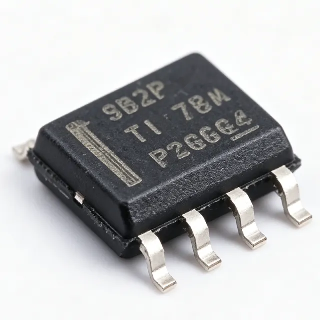
The TPS5430QDDARQ1 from Texas Instruments is an automotive-qualified (AEC-Q100) 3A step-down switching regulator in the SWIFT family, operating from a 5.5V to 36V input with an adjustable output from 1.221V to 31V at a fixed 500kHz switching frequency. It uses voltage-mode PWM control with an integrated high-side N-channel MOSFET and non-synchronous rectification, and it is rated from -40C to +125C in a thermally enhanced 8-pin HSOIC (DDA) PowerPAD package. As of 2026-09-04, the part is active and in stock at XAIPART with 99,999 units available, MOQ 1, priced at $3.45 for single units down to $1.95 at 1,000 units. It suits automotive infotainment, 24V industrial auxiliary supplies, USB charging ports, MCU point-of-load rails, and LED lighting power stages.
What Are the Quick Answers Buyers and Engineers Need About the TPS5430QDDARQ1?
Engineers evaluating this converter typically ask about input range, current capability, substitutes, thermal handling, and sourcing. The verified facts: input 5.5V-36V; output up to 3A continuous and adjustable 1.221V-31V; fixed 500kHz operation; AEC-Q100 qualified; cycle-by-cycle current limit and thermal shutdown built in; enable pin (ENA) for sequencing. Drop-in substitutes are limited to the TI TPS5430 family (TPS5430DDAR, TPS5430DDAG4, TPS5430MDDAREP); there is no true cross-brand pin-to-pin equivalent in the 8-pin DDA PowerPAD package. The TPS5450DDAR offers 5A in the same footprint but with different parameters and no automotive qualification. Pricing at XAIPART as of 2026-09-04: $3.45 (qty 1), $3.10 (10), $2.60 (100), $2.20 (500), $1.95 (1000). Full FAQ answers appear in the FAQ schema on this page and on the TPS5430QDDARQ1 product page.
How Do You Select and Design In the TPS5430QDDARQ1?
The TPS5430QDDARQ1 steps a higher DC input down to a lower regulated output using a high-side switch, an inductor, and an external rectifying element. Unlike a linear regulator, it achieves high efficiency by switching rather than dissipating excess power as heat. Internal compensation minimizes external component count, and the fixed 500kHz frequency permits a compact inductor.
Key design steps:
1. Verify input headroom. The 5.5V to 36V input range covers automotive 12V and 24V battery rails directly, with headroom for transients when paired with appropriate input protection. For 24V industrial rails, nominal tolerance fits inside the 36V maximum.
2. Set the output voltage. The VSENSE feedback pin references 1.221V. Set outputs from 1.221V up to approximately 31V with a resistor divider. For USB applications, a precise 5.0V or 5.1V setting is achieved via the divider.
3. Choose the external Schottky diode. Because the converter is non-synchronous, select a Schottky diode rated for the full 3A output current and the peak switch current. A low-leakage diode preserves efficiency at cold ambient temperatures in automotive lighting designs.
4. Plan the layout for EMI and thermals. Keep the PH node loop as small as possible for low EMI. Route the VSENSE trace away from the PH switch node to preserve regulation accuracy, especially for MCU core and I/O rails. The fixed 500kHz frequency allows predictable EMI placement and avoids variable-frequency EMI spikes that complicate system-level EMC testing.
5. Handle thermals with the PowerPAD. No separate heatsink is required: solder the DDA PowerPAD to a PCB thermal pad connected to a ground-plane copper pour. At high loads and large input-to-output voltage differentials, expand the copper area per the datasheet thermal layout guidance to keep the junction below 125C.
6. Use ENA for sequencing. Tie the enable pin (pin 4, floating enables the device) to a control signal or supervisor output for rail sequencing, such as headlamp on/off control or hot-swap-managed power-up. Refer to the official datasheet, titled '3-A WIDE-INPUT-RANGE STEP-DOWN SWIFT CONVERTER', on the TI TPS5430-Q1 product page; WEBENCH support and evaluation modules accelerate design cycles.
What Are the Key Pins of the TPS5430QDDARQ1 and How Should You Connect Them?
The 8-pin DDA PowerPAD pinout places BOOT (pin 1) for the high-side gate driver bootstrap, connected via a 0.01uF capacitor to PH. VSENSE (pin 3) is the feedback input with the 1.221V reference. ENA (pin 4) enables the device when floating. VIN (pin 5) accepts 5.5V to 36V. PH (pin 7) is the switch phase node connecting to the inductor and Schottky diode, and PWRGND (pin 8) is the power ground return. Solder the PowerPAD itself to the PCB ground plane for thermal dissipation. The full pin table with all connections lives on the product page.
Which Components Are Drop-In Alternatives to the TPS5430QDDARQ1?
Only TI TPS5430 family members are pin-compatible in the 8-pin DDA PowerPAD package. The TPS5430DDAR is the best drop-in replacement: it uses the identical die, same DDA package, and same pinout, but lacks AEC-Q100 qualification, so choose it for commercial/industrial builds only. The TPS5430DDAG4 is an alternate G4-suffix ordering variant of the same die, and the TPS5430MDDAREP is an enhanced-product (EP) variant for harsh environments sharing the same 3A/36V specs. The TPS5450DDAR provides 5A in the same footprint but with different parameters and no automotive qualification. No true cross-brand pin-to-pin equivalent exists; functionally similar wide-input 3A buck converters from other manufacturers use different pinouts and packages, requiring PCB redesign.
| Parameter | TPS5430QDDARQ1 | TPS5430DDAR | TPS5430DDAG4 | TPS5430MDDAREP | TPS5450DDAR |
|---|---|---|---|---|---|
| Topology | Step-Down (Buck) | Step-Down (Buck) | Step-Down (Buck) | Step-Down (Buck) | Step-Down (Buck) |
| Input Voltage Range | 5.5 V to 36 V | 5.5 V to 36 V | 5.5 V to 36 V | 5.5 V to 36 V | [DATA_NEEDED: TPS5450DDAR input voltage range] |
| Output Current | 3 A | 3 A | 3 A | 3 A | 5 A |
| Package | 8-Pin HSOIC (DDA) PowerPAD | 8-Pin HSOIC (DDA) PowerPAD | 8-Pin HSOIC (DDA) PowerPAD | 8-Pin HSOIC (DDA) PowerPAD | 8-Pin HSOIC (DDA) PowerPAD |
| AEC-Q100 Qualified | Yes | No | No | Enhanced Product (EP) for harsh environments | No |
| Drop-in Compatible | — | Yes (identical die/pinout) | Yes (G4 ordering variant) | Yes | Same footprint, different parameters |
| Best For | Automotive programs | Commercial/industrial builds | Non-automotive ordering | Harsh environments | Industrial 5A point-of-load |
What Applications Is the TPS5430QDDARQ1 Best Suited For?
Automotive infotainment and cluster power: AEC-Q100 qualification and the -40C to +125C range meet vehicle environmental requirements, while the 36V input withstands jump-start and transient conditions on 12V battery buses. Placed after battery input protection, it steps 13.5V nominal down to 5V or 3.3V; the 500kHz fixed frequency keeps the inductor compact.
Industrial 24V auxiliary supplies: The 5.5V-36V input covers nominal 24V rails with margin for PLC I/O modules, sensors, and interface boards. At 24V-to-5V/2A conversion, efficiency above 85% keeps thermal design straightforward, and the enable pin simplifies power-up sequencing.
USB charging ports: The 3A output covers single-port USB BC1.2 and high-current USB-C 5V/3A profiles directly from 12V or 24V battery input. Cycle-by-cycle current limiting protects against shorted cables, and the non-synchronous topology's free-wheeling Schottky simplifies BOM cost.
MCU point-of-load power: For C2000 MCU boards such as TMS320F28004x systems, it provides a robust 3.3V or 5V rail from 12V or 24V, with internal compensation reducing external parts on dense mixed-signal boards.
Automotive LED lighting: With ENA tied to a headlamp control signal, the converter provides clean on/off sequencing without a separate load switch; the 36V input supports load-dump robustness.
Server and networking backup rails: Fixed 500kHz operation avoids variable-frequency EMI spikes during system-level EMC testing, and thermal shutdown protects against fan-failure events.
What Does a Practical Design Solution Look Like?
Problem: Generate a stable 5V/2A auxiliary rail from a nominal 24V industrial rail for PLC I/O and interface loads, without a heatsink.
Approach: Use the TPS5430QDDARQ1 in a standard non-synchronous buck configuration. Its 36V maximum input covers 24V nominal with margin. Set the output to 5.0V via a VSENSE resistor divider referenced to 1.221V [VERIFY_NEEDED: exact divider resistor values - refer to datasheet application section]. Select a Schottky freewheel diode rated for 3A output and peak switch current. Solder the PowerPAD to a ground-plane copper pour sized per datasheet thermal guidance.
Results: At 24V-to-5V/2A conversion, efficiency above 85% keeps junction temperature well within the -40C to +125C rating, and cycle-by-cycle current limit plus thermal shutdown provide fault protection. [VERIFY_NEEDED: measured junction temperature for this specific condition - run thermal simulation or bench test per datasheet guidance.]
What Is the Market Position, Lifecycle Status, and Supply Situation for the TPS5430QDDARQ1?
The TPS5430QDDARQ1 is listed as active in lifecycle status, confirming Texas Instruments continues to manufacture it. As of 2026-09-04, XAIPART stocks 99,999 units with MOQ 1, and tiered pricing runs from $3.45 at qty 1 to $1.95 at qty 1000. Distributor channels including DigiKey and Mouser also carry the part; as of 2026-08-29, DigiKey listed it in stock with same-day shipping available for orders placed before cutoff. Automotive-qualified inventory can vary, so check real-time stock before committing to production builds. [DATA_NEEDED: long-term lifecycle forecast, last-time-buy dates, and multi-source supply data]
What Should Buyers Watch Next for the TPS5430QDDARQ1?
Anchor your decisions to the verified specs: the 36V input, 3A output, fixed 500kHz frequency, and AEC-Q100 qualification define where this part remains the right choice. For new automotive designs, confirm that 3A covers your rail budget; if you need more current in the same DDA footprint, the TPS5450DDAR offers 5A but is not automotive qualified, so evaluate TI's current automotive-qualified portfolio [VERIFY_NEEDED: current TI automotive 3A+ buck alternatives]. For non-automotive cost-sensitive builds, the pin-compatible TPS5430DDAR avoids paying the automotive-qualification premium. Watch pricing tiers: ordering at 500-1000 units cuts unit cost from $3.45 to $2.20-$1.95 as of 2026-09-04. Because stock levels for automotive-qualified parts fluctuate, secure allocation early for production programs and monitor the XAIPART product page for real-time availability.
Comments
Be the first to comment.
🔐 Please sign in to post a comment.
Don't have an account? Sign up