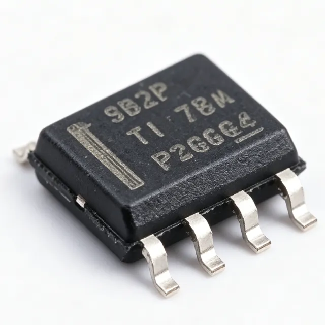
TPS5430QDDARQ1 - 3A, 36V Buck Converter AEC-Q100 | TI
MPN: TPS5430QDDARQ1 ✓ Active| Qty | Unit Price | Extended |
|---|---|---|
| 1 | $3.45 | $3.45 |
| 10 | $3.1 | $31.00 |
| 100 | $2.6 | $260.00 |
| 500 | $2.2 | $1,100.00 |
| 1,000 | $1.95 | $1,950.00 |
TPS5430QDDARQ1 Overview
A DC-DC buck converter is a type of switching voltage regulator that steps a higher DC input voltage down to a lower regulated output voltage using a high-side switch, an inductor, and a rectifying element. Buck converters sit within the broader hierarchy of power management ICs and, unlike linear regulators, achieve high efficiency by switching rather than dissipating excess power as heat.
Key features include up to 3A continuous output current, an adjustable output voltage from 1.221V to approximately 31V, voltage-mode PWM control with an integrated low-resistance high-side N-channel MOSFET, and non-synchronous rectification using an external Schottky diode. The 500kHz fixed frequency permits a compact inductor, while the internal compensation minimizes external component count. The PowerPAD package provides low thermal resistance for high-power-density designs.
According to the TI TPS5430-Q1 datasheet, the device integrates cycle-by-cycle current limiting, thermal shutdown, and an enable pin for rail sequencing. WEBENCH support and evaluation modules accelerate design cycles. The wide 36V input withstands automotive load-dump transients with modest protection, supporting battery-direct connections in 12V and 24V systems.
Typical applications include automotive infotainment and cluster power supplies, USB charging ports from battery rails, industrial 24V auxiliary supplies, and 5V/3.3V point-of-load conversions for MCUs and CAN transceivers.
Design consideration: because the converter is non-synchronous, select an external Schottky diode rated for the full output current and peak switch current, and keep the PH node loop as small as possible for low EMI.
Drop-in alternatives for TPS5430QDDARQ1 — same package, pin-to-pin compatible. Different-package parts requiring PCB rework are excluded.
Variants in this series
Same-series models that are drop-in compatible with TPS5430QDDARQ1 (same form factor and footprint) — differing in Package.
Quick Comparison Tool — Select alternative parts for side-by-side comparison:
TPS5430DDAR
✓ In Stock
$1.19 / Unit
View Datasheet →TPS5450DDAR
✓ In Stock
$2.55 / Unit
View Datasheet →TPS54331DR
✓ In Stock
$0.85 / Unit
View Datasheet →TPS5430DDAG4
📋 Reference alternative (not in catalog)
TPS5430MDDAREP
📋 Reference alternative (not in catalog)
TPS5430QDDARQ1 Maximum Ratings & Electrical Characteristics
| Topology | Step-Down (Buck) |
| Input Voltage Range | 5.5 V to 36 V |
| Output Voltage Range | 1.221 V to 31 V (adjustable) |
| Output Current | 3 A |
| Switching Frequency | 500 kHz (fixed) |
| Control Method | Voltage Mode PWM |
| Synchronous Rectifier | No |
| Number of Outputs | 1 |
| Package | 8-PowerSOIC / HSOIC (DDA), 3.90 mm width |
| Operating Temperature | -40C to +125C |
| Automotive Qualification | AEC-Q100 qualified |
| Enable Pin | Yes (ENA) |
| Protection | Cycle-by-cycle current limit, thermal shutdown |
| Mounting Type | Surface Mount |
| MSL Level | 2 (260C, 1 year) |
| RoHS Status | Compliant |
TPS5430QDDARQ1 Pin Configuration
| Pin 1 | BOOT — Bootstrap for high-side gate driver - connect 0.01uF capacitor to PH |
| Pin 2 | NC — No connection |
| Pin 3 | VSENSE — Feedback voltage sense input (1.221V reference) |
| Pin 4 | ENA — Enable input - floating enables the device |
| Pin 5 | VIN — Input supply, 5.5V to 36V |
| Pin 6 | NC — No connection |
| Pin 7 | PH — Switch phase node - to inductor and Schottky diode |
| Pin 8 | PWRGND — Power ground return |
Typical Applications
TPS5430QDDARQ1 is suitable for 6 applications: Automotive Infotainment Power, Industrial 24V Auxiliary Supply, USB Charging Ports, MCU Point-of-Load Power, Automotive LED Lighting Drivers, Server and Networking Backup Rails.
Automotive Infotainment Power
The TPS5430QDDARQ1 fits automotive infotainment and cluster power supplies because its AEC-Q100 qualification and -40C to +125C range meet vehicle environmental requirements, while the 36V input withstands jump-start and transient conditions on 12V battery buses. Its 3A output powers displays, audio amplifiers, and SoC rails. Placed directly after battery input protection, it steps 13.5V nominal down to 5V or 3.3V with high efficiency; the 500kHz fixed frequency keeps the inductor compact and outside the AM radio band edge concerns when frequency-planned.
Recommended
Industrial 24V Auxiliary Supply
The 5.5V to 36V input range covers nominal 24V industrial rails with margin for regulation tolerance, making the TPS5430QDDARQ1 a strong auxiliary supply for PLC I/O modules, sensors, and interface boards. Its 3A capability supports multiple downstream loads from a single converter, and the enable pin simplifies power-up sequencing. The PowerPAD package dissipates conversion losses into the PCB ground plane without a heatsink; at 24V-to-5V/2A conversion, efficiency above 85% keeps thermal design straightforward.
Recommended
USB Charging Ports
USB charging ports in vehicles and industrial equipment benefit from the TPS5430QDDARQ1's 3A output, which covers single-port USB BC1.2 and high-current USB-C 5V/3A profiles. Its wide input handles 12V or 24V battery input directly, and cycle-by-cycle current limiting protects against shorted cables. The adjustable 1.221V minimum feedback allows precise 5.0V or 5.1V setting via a resistor divider; the non-synchronous topology's free-wheeling Schottky diode avoids dead-time control complexity, simplifying BOM cost in charging applications.
Recommended
MCU Point-of-Load Power
For C2000 MCU boards such as TMS320F28004x systems, the TPS5430QDDARQ1 provides a robust 3.3V or 5V point-of-load from 12V or 24V rails. The 500kHz fixed frequency allows predictable EMI placement, and internal compensation reduces external component count on dense mixed-signal boards. Its 36V input tolerates supply surges that would exceed the absolute maximum of lower-voltage converters. Layout-wise, keeping the VSENSE trace away from the PH switch node preserves regulation accuracy for the MCU core and I/O rails.
Recommended
Automotive LED Lighting Drivers
The TPS5430QDDARQ1 supplies regulated rails for automotive LED lighting controllers and daytime-running-light modules. Its AEC-Q100 qualification, 36V input for load-dump robustness, and 3A output support LED string power stages or their control electronics. With the enable pin tied to a headlamp control signal, the converter provides clean on/off sequencing without a separate load switch. The non-synchronous buck with an external Schottky handles the wide temperature range; a low-leakage diode preserves efficiency at cold ambient temperatures.
Recommended
Server and Networking Backup Rails
In networking and server equipment, the TPS5430QDDARQ1 serves as a wide-input intermediate-bus or standby converter stepping 12V or 24V distribution rails to 5V or 3.3V auxiliary voltages for fans, controllers, and monitoring circuits. Its fixed 500kHz operation avoids variable-frequency EMI spikes that complicate system-level EMC testing, and the thermal shutdown protects against fan-failure events. The enable pin allows power sequencing managed by a hot-swap or supervisor device upstream of the converter.
Recommended
Recommended Products Summary
Engineering reference data for TPS5430QDDARQ1 — comparison, design guidance, and compliance information.
Selection Guide
Comparison with Alternatives
| Parameter | This Product | TPS5430DDAR | TPS5450DDAR | TPS5430MDDAREP | TPS54331DR |
|---|---|---|---|---|---|
| Package | HSOIC-8 PowerPAD (DDA) | HSOIC-8 PowerPAD (DDA) - same | HSOIC-8 PowerPAD (DDA) - same | HSOIC-8 PowerPAD (DDA) - same | SOIC-8 (D) - different footprint |
| Brand | Texas Instruments | Texas Instruments | Texas Instruments | Texas Instruments | Texas Instruments |
| Input Voltage Range | 5.5 V to 36 V | 5.5 V to 36 V | 5.5 V to 36 V | 5.5 V to 36 V | 3.5 V to 28 V |
| Output Current | 3 A | 3 A | 5 A | 3 A | 3 A |
| Switching Frequency | 500 kHz fixed | 500 kHz fixed | 500 kHz fixed | 500 kHz fixed | 570 kHz fixed |
| Automotive Grade | AEC-Q100 qualified | No | No | Enhanced Product (EP) | No |
| Operating Temperature | -40C to +125C | -40C to +125C | -40C to +125C | -40C to +125C | -40C to +125C |
| Control Method | Voltage Mode PWM, non-synchronous | Voltage Mode PWM, non-synchronous | Voltage Mode PWM, non-synchronous | Voltage Mode PWM, non-synchronous | Voltage Mode PWM, Eco-mode capable |
Key Differentiators
- AEC-Q100 automotive qualification (vs TPS5430DDAR)
- Wide 36V input in compact package (vs TPS54331DR)
- Lower cost for higher-current needs trade-off (vs TPS5450DDAR)
Design Notes
Minimize the PH loop consisting of VIN decoupling capacitor, PH pin, and free-wheeling Schottky diode - this is the highest dV/dt path and dominates radiated EMI. Place the Schottky diode anode and VIN ceramic cap within millimeters of the IC. Route VSENSE as a quiet Kelvin trace from the output capacitor, away from PH and BOOT nodes. Solder the PowerPAD to a ground pour with thermal vias per the TI TPS5430-Q1 datasheet layout section.
Select the external free-wheeling Schottky diode for at least 3A average current and reverse voltage above the 36V input plus margin (e.g., 40-60V rating, such as a 3A/45V Schottky). Low forward voltage and low reverse leakage directly improve efficiency, especially at high ambient temperature. Size the inductor for the peak switch current limit, not just the 3A load current, to avoid saturation during transients and startup.
Maximum dissipation concentrates in the internal high-side MOSFET and diode conduction losses. At 36V input, 5V output, and 3A load, duty cycle is roughly 14%, so diode conduction dominates; verify junction temperature using theta_JA with the PowerPAD soldered to at least the datasheet-recommended copper area. Without an adequate thermal pad, thermal shutdown around 150C will cause output dropout at high loads.
Compliance Information
RoHS compliant and MSL Level 2 (260C, 1 year) per distributor data (PartGenie). REACH, halogen-free, and conflict minerals status not stated in provided data.







