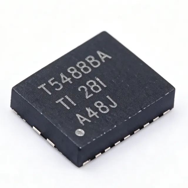
What Is the TPS548B28RWWR and What Can It Do for Your Design?
The Texas Instruments TPS548B28RWWR is a 2.7V to 16V input, 20A synchronous step-down (buck) converter with integrated MOSFETs, differential remote sense, and an internal 3V LDO, packaged in a 21-pin PowerVFQFN (RWW) surface-mount package. Its ±1% 0.6V voltage reference holds regulation accuracy over the full operating junction temperature range, making it a precise point-of-load (POL) solution for high-current computing loads. The output voltage range spans 0.6V to 5.5V, and the device operates from 4V to 16V input without external bias, extending down to 2.7V input with a 3.13V to 3.6V external bias. As of 2026-09-04, the TPS548B28RWWR is active (not discontinued) with 99,999 units in stock on XAIPART at $1 (qty ≥ 1), MOQ 1 — see the TPS548B28RWWR product page for live pricing.
Within the power management hierarchy, this single-channel buck sits between simple low-current bucks and multi-phase controllers. Integrated power MOSFETs — 7.7 mΩ high-side and 2.4 mΩ low-side RDS(on) — plus the D-CAP3-style control architecture minimize external component count while enabling fast load transients with low output capacitance, a combination well suited to space-constrained server, storage, and networking boards.
How Do You Select and Design In the TPS548B28RWWR? (Technical Guide)
Designing with the TPS548B28RWWR starts with confirming your input, output, and bias rails against the verified electrical limits. The device delivers up to 20A continuous output current from a 4V to 16V input in the standard configuration. If your rail runs below 4V — for example, a 3.3V intermediate bus — you can still use the part by supplying an external bias between 3.13V and 3.6V to the BIAS/VDD pin, which overrides the internal 3V LDO. This external bias override improves efficiency at lower input voltages because the internal LDO no longer drops the input supply to generate gate-drive power.
The 0.6V ±1% reference defines your minimum output voltage, and the programmable output range extends to 5.5V. Set the feedback divider from your target VOUT back to the reference. Because the part provides differential remote sense, route the sense lines as a Kelvin pair directly to the load point (FPGA, ASIC, or processor core) rather than to the converter output caps; this compensates for PCB IR drop at 20A loads, where even a few milliohms of trace resistance translates into tens of millivolts of droop — far more than the ±1% regulation budget.
For light-load behavior, choose between Skip-mode and forced-CCM (FCCM) operation. Skip-mode maximizes light-load efficiency for bursty computing loads; FCCM holds a constant switching frequency, which simplifies output ripple prediction and avoids frequency variation in sensitive analog rails [VERIFY_NEEDED: switching frequency values and mode selection method].
Fault handling is built in: hiccup-mode current limit protects against short circuits by retrying after a pause, and programmable soft start controls inrush during power-up — important when sequencing multiple POL rails on a server board.
Layout Guidance for 20A Operation
At 20A continuous, layout quality determines both thermal and EMI performance. Keep the input capacitor loop (input caps → high-side FET → low-side FET → return) as tight as possible, and minimize SW-node copper area to control radiated EMI. Use solid ground planes under the QFN for heat spreading, since total conduction plus switching losses concentrate in the small 21-pin PowerVFQFN footprint [VERIFY_NEEDED: thermal resistance values for the RWW package]. TI provides the TPS548B28EVM-023 evaluation module as a reference layout — start from it rather than re-deriving the power stage.
What Are the Drop-In Alternatives to the TPS548B28RWWR?
No alternative component data is provided in the verified database for this article, so a cross-competitor comparison cannot be made without fabricating specifications. The table below consolidates the verified specifications of the TPS548B28RWWR itself as the authoritative reference. For a true alternatives analysis with verified part-to-part data, [DATA_NEEDED: comparable 16V-input, 20A-class synchronous buck converters with verified specifications].
| Parameter | TPS548B28RWWR |
|---|---|
| Topology | Synchronous step-down (buck) |
| Input voltage (no external bias) | 4 V to 16 V |
| Input voltage (with external bias) | 2.7 V to 16 V |
| External bias range | 3.13 V to 3.6 V |
| Maximum output current | 20 A |
| Output voltage range | 0.6 V to 5.5 V |
| Reference voltage | 0.6 V ±1% over junction temperature |
| High-side RDS(on) | 7.7 mΩ |
| Low-side RDS(on) | 2.4 mΩ |
| Remote sense | Differential |
| Light-load mode | Skip-mode or FCCM (selectable) |
| Current limit | Hiccup mode |
| Soft start | Programmable |
| Internal LDO | 3 V |
| Package | 21-PowerVFQFN (RWW) |
| Lifecycle status | Active |
What Is the Market Position, Lifecycle Status, and Supply Situation for the TPS548B28RWWR?
According to the XAIPART product database, the TPS548B28RWWR carries an active lifecycle status, indicating Texas Instruments continues to manufacture the part with no end-of-life announcement in the verified record. Supply is currently strong: 99,999 units are in stock as of 2026-09-04, with pricing at $1 per unit (qty ≥ 1) and MOQ of 1, so both prototype quantities and volume orders can be fulfilled immediately. [DATA_NEEDED: unit shipment volume, market share data, and TI roadmap commentary]. For current stock and lead times, check the product page on XAIPART or browse other DC-DC converters in stock.
What Trends Should Buyers Watch for 20A Point-of-Load Power?
Three trends anchored to the TPS548B28RWWR's verified feature set deserve buyer attention. First, integration density: the combination of 7.7 mΩ high-side and 2.4 mΩ low-side integrated MOSFETs in a single compact QFN eliminates external FET selection and layout risk — expect more demand shifting toward integrated-FET bucks as datacenter board space tightens. Second, regulation accuracy at the load: the ±1% 0.6V reference combined with differential remote sense reflects the industry push toward lower core voltages, where every millivolt of margin costs efficiency; designs targeting 0.6V-class rails benefit directly. Third, flexibility at low bus voltages: extended 2.7V operation via the 3.13V–3.6V external bias range lets one part serve both 12V and 3.3V intermediate-bus architectures, consolidating the BOM. Buy on verified stock data — with 99,999 units available as of 2026-09-04 at $1, there is no current shortage pressure on this SKU.
Related reading: see our guide to how to select synchronous buck converters for the full selection methodology.
Comments
Be the first to comment.
🔐 Please sign in to post a comment.
Don't have an account? Sign up