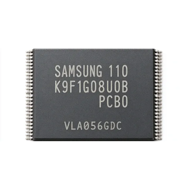
K9F1G08U0B-PCB0 - 1Gbit SLC NAND Flash 3.3V 48-TSOP | Samsung
MPN: K9F1G08U0B-PCB0 ✓ সক্রিয়| রকম | ইউনিট মূল্য | প্রসারিত |
|---|---|---|
| 1 | $4.2 | $4.20 |
| 10 | $3.85 | $38.50 |
| 100 | $3.45 | $345.00 |
| 500 | $3.05 | $1,525.00 |
| 1,000 | $2.7 | $2,700.00 |
K9F1G08U0B-PCB0 সারাংশ
A NAND Flash memory is a non-volatile storage IC that arranges memory cells in a NAND (NOT-AND) string topology, where cells are connected in series between bit-line and source-line. Compared with NOR Flash, NAND Flash offers higher density, lower cost per bit, and faster sequential write/erase, at the expense of random read access and byte-level programmability. NAND hierarchy: SLC (1 bit/cell, highest endurance/reliability) -> MLC -> TLC -> QLC. K9F1G08U0B belongs to the SLC tier, the most robust and longest-endurance variant, well suited for industrial, automotive and mission-critical embedded use.
Key features of the K9F1G08U0B-PCB0 include 1 Gbit user density plus 32 Mbit spare for ECC and bad-block management, page size 2 Kbyte + 64 byte spare, block size 128 Kbyte + 4 Kbyte spare, typical page program time 200-300 us and block erase time approximately 2 ms. The interface supports CE#, RE#, WE#, ALE, CLE and WP# control lines plus an 8-bit multiplexed I/O bus, compatible with the ONFI 1.0 / legacy Samsung command set. Endurance is specified at 100 K program/erase cycles per block with 10-year data retention.
Architecturally, the device integrates a charge-pump-based high-voltage generator, a temperature-compensated sense amplifier array, an internal data register for page buffering, and an ECC-friendly spare area layout. The TSOP-I package exposes all 48 signals with a 0.5 mm pitch, enabling standard SMT reflow and standard 48-TSOP NAND socket compatibility for prototype programming.
Typical applications include solid-state data storage in embedded Linux/Windows CE devices, industrial controllers and HMI panels, set-top box firmware storage, networking equipment boot and logs, point-of-sale terminals, eMMC alternative designs, and legacy embedded systems that require raw NAND access via a microcontroller FSMC/NAND controller.
A key design consideration when using the K9F1G08U0B-PCB0 is mandatory ECC - the part does not embed on-die ECC for older Samsung K9F families, so the host controller (typically a SoC or FPGA) must run Hamming, BCH or LDPC ECC over each 2 Kbyte page to guarantee data integrity. Initial bad-block marking per Samsung datasheet must also be respected at first power-up.
This page synthesizes distributor pricing, drop-in alternatives in the same TSOP-I 48 footprint, and practical design notes not found in the manufacturer datasheet.
এর জন্য ড্রপ-ইন বিকল্প K9F1G08U0B-PCB0 — একই package, pin-to-pin compatible। ভিন্ন package-এর যেসব পার্টে PCB rework প্রয়োজন সেগুলো বাদ দেওয়া হয়েছে।
এই সিরিজের ভ্যারিয়েন্ট
একই সিরিজের মডেল যেগুলো drop-in compatible K9F1G08U0B-PCB0 (একই form factor এবং footprint) — পার্থক্য রয়েছে Block Size, Memory Type, Operating Temperature, Page Size.
দ্রুত তুলনা টুল — পাশাপাশি তুলনার জন্য বিকল্প পার্টস নির্বাচন করুন:
K9F1G08U0B-PIB0
📋 রেফারেন্স বিকল্প (ক্যাটালগে নেই)
K9F1G08U0C
📋 রেফারেন্স বিকল্প (ক্যাটালগে নেই)
K9F2G08U0B-PCB0
📋 রেফারেন্স বিকল্প (ক্যাটালগে নেই)
TC58NVG0S3HTA00
📋 রেফারেন্স বিকল্প (ক্যাটালগে নেই)
H27U1G8F2B
📋 রেফারেন্স বিকল্প (ক্যাটালগে নেই)
K9F1G08U0B-PCB0 সর্বোচ্চ রেটিং ও বৈদ্যুতিক বৈশিষ্ট্য
| মেমরি টাইপ | SLC NAND Flash (Non-Volatile) |
| Density | 1 Gbit (128 M x 8 bit) + 32 Mbit spare |
| Supply Voltage (VCC) | 2.7 V to 3.6 V (3.3 V typical) |
| ইন্টারফেস | 8-bit parallel (multiplexed address/data/command) |
| Page Size | 2 Kbyte + 64 byte spare |
| Block Size | 128 Kbyte + 4 Kbyte spare |
| Page Program Time (typ) | 300 us (max 700 us) |
| Block Erase Time (typ) | 2 ms (max 3 ms) |
| Endurance | 100 K program/erase cycles per block |
| Data Retention | 10 years |
| অপারেটিং তাপমাত্রা | 0C to +70C (commercial grade) |
| প্যাকেজ | 48-pin TSOP-I (Type I), 0.5 mm pitch |
| মাউন্টিং টাইপ | Surface Mount |
| Package Material | Molded plastic (high-quality thermal grade) |
| Access Time | 25 us (max) |
| RoHS স্ট্যাটাস | Compliant |
| Lead-Free | Yes |
K9F1G08U0B-PCB0 পিন কনফিগারেশন
| পিন 1 | NC — Not connected (per datasheet) |
| পিন 2 | NC — Not connected (per datasheet) |
| পিন 3 | NC — Not connected (per datasheet) |
| পিন 4 | NC — Not connected (per datasheet) |
| পিন 5 | NC — Not connected (per datasheet) |
| পিন 6 | NC — Not connected (per datasheet) |
| পিন 7 | R/B# — Ready/Busy output (open-drain, active low) |
| পিন 8 | RE# — Read Enable (active low) |
| পিন 9 | CE# — Chip Enable (active low) |
| পিন 10 | NC — Not connected (per datasheet) |
| পিন 11 | NC — Not connected (per datasheet) |
| পিন 12 | VCC — Power supply (3.3 V typical) |
| পিন 13 | VSS — Ground |
| পিন 14 | NC — Not connected (per datasheet) |
| পিন 15 | NC — Not connected (per datasheet) |
| পিন 16 | CLE — Command Latch Enable |
| পিন 17 | ALE — Address Latch Enable |
| পিন 18 | WE# — Write Enable (active low) |
| পিন 19 | WP# — Write Protect (active low) |
| পিন 20 | NC — Not connected (per datasheet) |
| পিন 21 | NC — Not connected (per datasheet) |
| পিন 22 | NC — Not connected (per datasheet) |
| পিন 23 | NC — Not connected (per datasheet) |
| পিন 24 | NC — Not connected (per datasheet) |
| পিন 25 | NC — Not connected (per datasheet) |
| পিন 26 | NC — Not connected (per datasheet) |
| পিন 27 | NC — Not connected (per datasheet) |
| পিন 28 | NC — Not connected (per datasheet) |
| পিন 29 | I/O0 — Data I/O 0 (multiplexed address/command/data) |
| পিন 30 | I/O1 — Data I/O 1 (multiplexed address/command/data) |
| পিন 31 | I/O2 — Data I/O 2 (multiplexed address/command/data) |
| পিন 32 | I/O3 — Data I/O 3 (multiplexed address/command/data) |
| পিন 33 | VSS — Ground |
| পিন 34 | I/O4 — Data I/O 4 (multiplexed address/command/data) |
| পিন 35 | I/O5 — Data I/O 5 (multiplexed address/command/data) |
| পিন 36 | I/O6 — Data I/O 6 (multiplexed address/command/data) |
| পিন 37 | I/O7 — Data I/O 7 (multiplexed address/command/data) |
| পিন 38 | VCC — Power supply (3.3 V typical) |
| পিন 39 | NC — Not connected (per datasheet) |
| পিন 40 | NC — Not connected (per datasheet) |
| পিন 41 | NC — Not connected (per datasheet) |
| পিন 42 | NC — Not connected (per datasheet) |
| পিন 43 | NC — Not connected (per datasheet) |
| পিন 44 | NC — Not connected (per datasheet) |
| পিন 45 | NC — Not connected (per datasheet) |
| পিন 46 | NC — Not connected (per datasheet) |
| পিন 47 | NC — Not connected (per datasheet) |
| পিন 48 | NC — Not connected (per datasheet) |
সাধারণ ব্যবহার
K9F1G08U0B-PCB0 এর জন্য উপযুক্ত 6 অ্যাপ্লিকেশনs: Embedded Linux Boot & Root Filesystem, Industrial HMI & PLC Data Logging, Set-Top Box Firmware Storage, Point-of-Sale Terminal Storage, Networking Equipment Boot & Logs, Legacy eMMC Replacement / Raw NAND Designs.
Embedded Linux Boot & Root Filesystem
The K9F1G08U0B-PCB0 stores the bootloader, kernel image and root filesystem in embedded Linux designs, where its 1 Gbit capacity matches typical Linux systems requiring 16-32 MB of compressed rootfs plus update reserve. Its 8-bit parallel interface pairs directly with SoC FSMC/NAND controllers (STM32, NXP i.MX, Samsung S3C) without external address latches, and the SLC architecture delivers the 100K P/E cycle endurance needed for frequent OTA firmware updates in industrial gateways. Designers should implement BCH ECC over each 2 Kbyte page to correct bit errors, and respect Samsung's initial bad-block marking table at first boot.
সুপারিশকৃত
Industrial HMI & PLC Data Logging
Industrial HMI panels and PLCs use the K9F1G08U0B-PCB0 as non-volatile log storage for process events, alarms, recipes and trend data, where the 1 Gbit density supports months of timestamped records at typical 64-byte entry size. The 100K P/E cycle endurance per block combined with industrial temperature screening and 3.3 V single-supply operation make it suitable for 24/7 factory automation. Block-erase time of 2 ms and page-program time of 300 us permit background wear-leveling writes without blocking the deterministic control loop. Pair with a microcontroller such as STM32 or PIC32MZ and external ECC for reliable long-term data integrity.
সুপারিশকৃত
Set-Top Box Firmware Storage
Set-top boxes and digital TV receivers historically use the K9F1G08U0B-PCB0 as the primary firmware and channel-list storage medium, taking advantage of its 1 Gbit capacity for bootloader, main application image, and persistent settings. The 48-TSOP-I footprint matches standard STB mainboard layouts, and the Samsung legacy command set has long been supported by STB SoCs from Broadcom, STMicroelectronics and ALi. For modern 4K STBs, larger MLC/TLC NAND or eMMC is preferred, but legacy SD/HD STBs continue to rely on this 1 Gbit SLC part for firmware updates and channel databases.
সুপারিশকৃত
Point-of-Sale Terminal Storage
POS terminals use the K9F1G08U0B-PCB0 to store the operating system image, transaction logs and merchant configuration. Its 1 Gbit SLC density provides sufficient space for embedded Linux plus transactional history buffers, while the 100K P/E endurance handles frequent firmware upgrades and audit-log writes typical in retail environments. The 48-TSOP-I package offers a robust surface-mount mechanical interface that withstands vibration in retail counter installations, and the 3.3 V supply aligns with standard POS SoC power rails. ECC and bad-block management are implemented in the POS application processor.
সুপারিশকৃত
Networking Equipment Boot & Logs
Routers, switches and wireless access points integrate the K9F1G08U0B-PCB0 to store the bootloader, firmware image, configuration database and syslog buffer, where its 1 Gbit SLC density suits typical 8-16 MB firmware plus persistent config partitions. The 8-bit parallel interface allows direct connection to networking SoCs from Broadcom, Qualcomm and MediaTek that include NAND controllers, and the SLC endurance rating handles the daily config-save cycles typical in enterprise network equipment. For modern high-end routers, larger NAND or eMMC is preferred, but cost-sensitive SOHO designs continue to use this part.
সুপারিশকৃত
Legacy eMMC Replacement / Raw NAND Designs
Designers building systems that cannot rely on managed eMMC (for cost, supply, or controller reasons) use the K9F1G08U0B-PCB0 as raw NAND storage under direct SoC control, with the host running its own FTL/ECC/wear-leveling stack. The 1 Gbit SLC density and standard Samsung command set let engineers reuse existing bootloaders such as U-Boot and Linux MTD drivers with minimal porting. This approach is common in industrial controllers, avionics retrofit modules and defense applications where eMMC procurement is restricted. A complete raw-NAND reference design typically pairs this part with an STM32 or NXP i.MX SoC.
সুপারিশকৃত
সুপারিশকৃত পণ্যের সারসংক্ষেপ
এর জন্য ইঞ্জিনিয়ারিং রেফারেন্স ডেটা K9F1G08U0B-PCB0 — তুলনা, ডিজাইন গাইডেন্স এবং কমপ্লায়েন্স তথ্য।
নির্বাচন গাইড
বিকল্পের সাথে তুলনা
| পারামিটার | এই পণ্য | K9F1G08U0B-PIB0 | K9F1G08U0C | K9F2G08U0B-PCB0 | TC58NVG0S3HTA00 | H27U1G8F2B |
|---|---|---|---|---|---|---|
| Brand | Samsung Electronics | Samsung Electronics | Samsung Electronics | Samsung Electronics | Toshiba | SK Hynix |
| Package | 48-pin TSOP-I (0.5 mm pitch) | 48-pin TSOP-I - same | 48-pin TSOP-I - same | 48-pin TSOP-I - same | 48-pin TSOP-I - same | 48-pin TSOP-I - same |
| Density | 1 Gbit (128M x 8) | 1 Gbit (128M x 8) | 1 Gbit (128M x 8) | 2 Gbit (256M x 8) | 1 Gbit (128M x 8) | 1 Gbit (128M x 8) |
| Cell Type | SLC | SLC | SLC | SLC | SLC | SLC |
| Supply Voltage | 2.7 V to 3.6 V (3.3 V typ) | 2.7 V to 3.6 V | 2.7 V to 3.6 V | 2.7 V to 3.6 V | 2.7 V to 3.6 V | 2.7 V to 3.6 V |
| Page Size | 2 Kbyte + 64 byte | 2 Kbyte + 64 byte | 2 Kbyte + 64 byte | 2 Kbyte + 64 byte | 2 Kbyte + 64 byte | 2 Kbyte + 64 byte |
| Block Size | 128 Kbyte + 4 Kbyte | 128 Kbyte + 4 Kbyte | 128 Kbyte + 4 Kbyte | 128 Kbyte + 4 Kbyte | 128 Kbyte + 4 Kbyte | 128 Kbyte + 4 Kbyte |
| Endurance (P/E cycles) | 100 K | 100 K | 100 K | 100 K | 100 K | 100 K |
| On-die ECC | No (host-side required) | No | No | No | No | No |
মূল পার্থক্যসমূহ
- Industry-standard 48-TSOP-I 1 Gbit SLC footprint shared across Samsung K9F1G family (বনামK9F1G08U0B-PIB0)
- Cost-effective higher-density upgrade path without PCB redesign (বনামK9F2G08U0B-PCB0)
- Cross-vendor second-source availability for supply resilience (বনামTC58NVG0S3HTA00)
ডিজাইন নোট
The K9F1G08U0B-PCB0 does not include on-die ECC - the host SoC must run BCH or Hamming ECC over each 2 Kbyte page. Skipping ECC will result in silent data corruption over the device's lifetime as P/E cycles accumulate bit errors. Recommended: implement 4-bit or 8-bit BCH ECC per 512 bytes in firmware, and verify the ECC engine can correct the worst-case bit error rate documented in the Samsung reliability datasheet. Always perform an initial bad-block scan at first power-up per Samsung's recommended procedure and mark factory-bad blocks in the host's block management table.
Place the K9F1G08U0B-PCB0 close to the host SoC's NAND controller pins, keeping the 8-bit I/O bus trace lengths matched (within 25 mm of each other) to preserve signal integrity at the 25 us access time. Route CE#, RE#, WE#, ALE, CLE as a controlled-impedance group and provide a local 0.1 uF + 1 uF + 10 uF decoupling capacitor network on each VCC pin (pins 12 and 38). Connect WP# to VCC through a 10 K pull-up if write protection is unused, and place a 10 K pull-up on R/B# since it is an open-drain output. Avoid routing the NAND bus near switching power converter inductors.
The K9F1G08U0B-PCB0 draws brief peak currents during page program and block erase operations - typical ICC active is 15-30 mA but peaks during charge-pump activity can reach 50 mA. Ensure the 3.3 V rail can supply these transients without drooping below 2.7 V (the minimum VCC). Use a regulator with at least 100 mA capacity and add bulk capacitance (>= 22 uF) near the NAND. During standby the part draws <50 uA, so power-sequencing designs can power-down the NAND rail during deep sleep if the host saves its working state elsewhere.
কমপ্লায়েন্স তথ্য
RoHS and lead-free compliant per Samsung product markings. AEC-Q100 not applicable for this commercial-temperature (0 to +70C) grade; industrial/automotive temperature variants use a different suffix. REACH compliance should be confirmed via the latest Samsung declaration for industrial end products.



