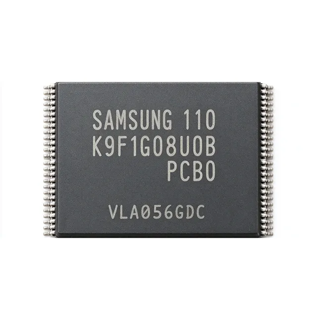
K9F1G08U0B-PCB0 - 1Gbit SLC NAND Flash 3.3V 48-TSOP | Samsung
MPN: K9F1G08U0B-PCB0 ✓ فعال| مقدار | فی یونٹ قیمت | کل رقم |
|---|---|---|
| 1 | $4.2 | $4.20 |
| 10 | $3.85 | $38.50 |
| 100 | $3.45 | $345.00 |
| 500 | $3.05 | $1,525.00 |
| 1,000 | $2.7 | $2,700.00 |
K9F1G08U0B-PCB0 جائزہ
A NAND Flash memory is a non-volatile storage IC that arranges memory cells in a NAND (NOT-AND) string topology, where cells are connected in series between bit-line and source-line. Compared with NOR Flash, NAND Flash offers higher density, lower cost per bit, and faster sequential write/erase, at the expense of random read access and byte-level programmability. NAND hierarchy: SLC (1 bit/cell, highest endurance/reliability) -> MLC -> TLC -> QLC. K9F1G08U0B belongs to the SLC tier, the most robust and longest-endurance variant, well suited for industrial, automotive and mission-critical embedded use.
Key features of the K9F1G08U0B-PCB0 include 1 Gbit user density plus 32 Mbit spare for ECC and bad-block management, page size 2 Kbyte + 64 byte spare, block size 128 Kbyte + 4 Kbyte spare, typical page program time 200-300 us and block erase time approximately 2 ms. The interface supports CE#, RE#, WE#, ALE, CLE and WP# control lines plus an 8-bit multiplexed I/O bus, compatible with the ONFI 1.0 / legacy Samsung command set. Endurance is specified at 100 K program/erase cycles per block with 10-year data retention.
Architecturally, the device integrates a charge-pump-based high-voltage generator, a temperature-compensated sense amplifier array, an internal data register for page buffering, and an ECC-friendly spare area layout. The TSOP-I package exposes all 48 signals with a 0.5 mm pitch, enabling standard SMT reflow and standard 48-TSOP NAND socket compatibility for prototype programming.
Typical applications include solid-state data storage in embedded Linux/Windows CE devices, industrial controllers and HMI panels, set-top box firmware storage, networking equipment boot and logs, point-of-sale terminals, eMMC alternative designs, and legacy embedded systems that require raw NAND access via a microcontroller FSMC/NAND controller.
A key design consideration when using the K9F1G08U0B-PCB0 is mandatory ECC - the part does not embed on-die ECC for older Samsung K9F families, so the host controller (typically a SoC or FPGA) must run Hamming, BCH or LDPC ECC over each 2 Kbyte page to guarantee data integrity. Initial bad-block marking per Samsung datasheet must also be respected at first power-up.
This page synthesizes distributor pricing, drop-in alternatives in the same TSOP-I 48 footprint, and practical design notes not found in the manufacturer datasheet.
کے لیے ڈراپ اِن متبادل K9F1G08U0B-PCB0 — یکساں پیکیج، پن سے پن مطابقت پذیر۔ مختلف پیکیج والے پرزے جن کے لیے PCB دوبارہ کام درکار ہو، شامل نہیں ہیں۔
اس سیریز میں مختلف ورژن
اسی سیریز کے ماڈلز جو ڈراپ اِن مطابقت رکھتے ہیں K9F1G08U0B-PCB0 (یکساں فارم فیکٹر اور فٹ پرنٹ) — میں مختلف Block Size, Memory Type, Operating Temperature, Page Size.
فوری موازنہ ٹول — ساتھ ساتھ موازنے کے لیے متبادل پرزے منتخب کریں:
K9F1G08U0B-PIB0
📋 حوالہ جاتی متبادل (کیٹلاگ میں نہیں)
K9F1G08U0C
📋 حوالہ جاتی متبادل (کیٹلاگ میں نہیں)
K9F2G08U0B-PCB0
📋 حوالہ جاتی متبادل (کیٹلاگ میں نہیں)
TC58NVG0S3HTA00
📋 حوالہ جاتی متبادل (کیٹلاگ میں نہیں)
H27U1G8F2B
📋 حوالہ جاتی متبادل (کیٹلاگ میں نہیں)
K9F1G08U0B-PCB0 زیادہ سے زیادہ ریٹنگز اور برقی خصوصیات
| میموری ٹائپ | SLC NAND Flash (Non-Volatile) |
| Density | 1 Gbit (128 M x 8 bit) + 32 Mbit spare |
| Supply Voltage (VCC) | 2.7 V to 3.6 V (3.3 V typical) |
| انٹرفیس | 8-bit parallel (multiplexed address/data/command) |
| Page Size | 2 Kbyte + 64 byte spare |
| Block Size | 128 Kbyte + 4 Kbyte spare |
| Page Program Time (typ) | 300 us (max 700 us) |
| Block Erase Time (typ) | 2 ms (max 3 ms) |
| Endurance | 100 K program/erase cycles per block |
| Data Retention | 10 years |
| آپریٹنگ درجہ حرارت | 0C to +70C (commercial grade) |
| پیکیج | 48-pin TSOP-I (Type I), 0.5 mm pitch |
| ماؤنٹنگ ٹائپ | Surface Mount |
| Package Material | Molded plastic (high-quality thermal grade) |
| Access Time | 25 us (max) |
| RoHS اسٹیٹس | Compliant |
| Lead-Free | Yes |
K9F1G08U0B-PCB0 پن کنفیگریشن
| پن 1 | NC — Not connected (per datasheet) |
| پن 2 | NC — Not connected (per datasheet) |
| پن 3 | NC — Not connected (per datasheet) |
| پن 4 | NC — Not connected (per datasheet) |
| پن 5 | NC — Not connected (per datasheet) |
| پن 6 | NC — Not connected (per datasheet) |
| پن 7 | R/B# — Ready/Busy output (open-drain, active low) |
| پن 8 | RE# — Read Enable (active low) |
| پن 9 | CE# — Chip Enable (active low) |
| پن 10 | NC — Not connected (per datasheet) |
| پن 11 | NC — Not connected (per datasheet) |
| پن 12 | VCC — Power supply (3.3 V typical) |
| پن 13 | VSS — Ground |
| پن 14 | NC — Not connected (per datasheet) |
| پن 15 | NC — Not connected (per datasheet) |
| پن 16 | CLE — Command Latch Enable |
| پن 17 | ALE — Address Latch Enable |
| پن 18 | WE# — Write Enable (active low) |
| پن 19 | WP# — Write Protect (active low) |
| پن 20 | NC — Not connected (per datasheet) |
| پن 21 | NC — Not connected (per datasheet) |
| پن 22 | NC — Not connected (per datasheet) |
| پن 23 | NC — Not connected (per datasheet) |
| پن 24 | NC — Not connected (per datasheet) |
| پن 25 | NC — Not connected (per datasheet) |
| پن 26 | NC — Not connected (per datasheet) |
| پن 27 | NC — Not connected (per datasheet) |
| پن 28 | NC — Not connected (per datasheet) |
| پن 29 | I/O0 — Data I/O 0 (multiplexed address/command/data) |
| پن 30 | I/O1 — Data I/O 1 (multiplexed address/command/data) |
| پن 31 | I/O2 — Data I/O 2 (multiplexed address/command/data) |
| پن 32 | I/O3 — Data I/O 3 (multiplexed address/command/data) |
| پن 33 | VSS — Ground |
| پن 34 | I/O4 — Data I/O 4 (multiplexed address/command/data) |
| پن 35 | I/O5 — Data I/O 5 (multiplexed address/command/data) |
| پن 36 | I/O6 — Data I/O 6 (multiplexed address/command/data) |
| پن 37 | I/O7 — Data I/O 7 (multiplexed address/command/data) |
| پن 38 | VCC — Power supply (3.3 V typical) |
| پن 39 | NC — Not connected (per datasheet) |
| پن 40 | NC — Not connected (per datasheet) |
| پن 41 | NC — Not connected (per datasheet) |
| پن 42 | NC — Not connected (per datasheet) |
| پن 43 | NC — Not connected (per datasheet) |
| پن 44 | NC — Not connected (per datasheet) |
| پن 45 | NC — Not connected (per datasheet) |
| پن 46 | NC — Not connected (per datasheet) |
| پن 47 | NC — Not connected (per datasheet) |
| پن 48 | NC — Not connected (per datasheet) |
عام استعمالات
K9F1G08U0B-PCB0 کے لیے موزوں ہے 6 ایپلیکیشنs: Embedded Linux Boot & Root Filesystem, Industrial HMI & PLC Data Logging, Set-Top Box Firmware Storage, Point-of-Sale Terminal Storage, Networking Equipment Boot & Logs, Legacy eMMC Replacement / Raw NAND Designs.
Embedded Linux Boot & Root Filesystem
The K9F1G08U0B-PCB0 stores the bootloader, kernel image and root filesystem in embedded Linux designs, where its 1 Gbit capacity matches typical Linux systems requiring 16-32 MB of compressed rootfs plus update reserve. Its 8-bit parallel interface pairs directly with SoC FSMC/NAND controllers (STM32, NXP i.MX, Samsung S3C) without external address latches, and the SLC architecture delivers the 100K P/E cycle endurance needed for frequent OTA firmware updates in industrial gateways. Designers should implement BCH ECC over each 2 Kbyte page to correct bit errors, and respect Samsung's initial bad-block marking table at first boot.
تجویز کردہ
Industrial HMI & PLC Data Logging
Industrial HMI panels and PLCs use the K9F1G08U0B-PCB0 as non-volatile log storage for process events, alarms, recipes and trend data, where the 1 Gbit density supports months of timestamped records at typical 64-byte entry size. The 100K P/E cycle endurance per block combined with industrial temperature screening and 3.3 V single-supply operation make it suitable for 24/7 factory automation. Block-erase time of 2 ms and page-program time of 300 us permit background wear-leveling writes without blocking the deterministic control loop. Pair with a microcontroller such as STM32 or PIC32MZ and external ECC for reliable long-term data integrity.
تجویز کردہ
Set-Top Box Firmware Storage
Set-top boxes and digital TV receivers historically use the K9F1G08U0B-PCB0 as the primary firmware and channel-list storage medium, taking advantage of its 1 Gbit capacity for bootloader, main application image, and persistent settings. The 48-TSOP-I footprint matches standard STB mainboard layouts, and the Samsung legacy command set has long been supported by STB SoCs from Broadcom, STMicroelectronics and ALi. For modern 4K STBs, larger MLC/TLC NAND or eMMC is preferred, but legacy SD/HD STBs continue to rely on this 1 Gbit SLC part for firmware updates and channel databases.
تجویز کردہ
Point-of-Sale Terminal Storage
POS terminals use the K9F1G08U0B-PCB0 to store the operating system image, transaction logs and merchant configuration. Its 1 Gbit SLC density provides sufficient space for embedded Linux plus transactional history buffers, while the 100K P/E endurance handles frequent firmware upgrades and audit-log writes typical in retail environments. The 48-TSOP-I package offers a robust surface-mount mechanical interface that withstands vibration in retail counter installations, and the 3.3 V supply aligns with standard POS SoC power rails. ECC and bad-block management are implemented in the POS application processor.
تجویز کردہ
Networking Equipment Boot & Logs
Routers, switches and wireless access points integrate the K9F1G08U0B-PCB0 to store the bootloader, firmware image, configuration database and syslog buffer, where its 1 Gbit SLC density suits typical 8-16 MB firmware plus persistent config partitions. The 8-bit parallel interface allows direct connection to networking SoCs from Broadcom, Qualcomm and MediaTek that include NAND controllers, and the SLC endurance rating handles the daily config-save cycles typical in enterprise network equipment. For modern high-end routers, larger NAND or eMMC is preferred, but cost-sensitive SOHO designs continue to use this part.
تجویز کردہ
Legacy eMMC Replacement / Raw NAND Designs
Designers building systems that cannot rely on managed eMMC (for cost, supply, or controller reasons) use the K9F1G08U0B-PCB0 as raw NAND storage under direct SoC control, with the host running its own FTL/ECC/wear-leveling stack. The 1 Gbit SLC density and standard Samsung command set let engineers reuse existing bootloaders such as U-Boot and Linux MTD drivers with minimal porting. This approach is common in industrial controllers, avionics retrofit modules and defense applications where eMMC procurement is restricted. A complete raw-NAND reference design typically pairs this part with an STM32 or NXP i.MX SoC.
تجویز کردہ
تجویز کردہ پروڈکٹس کا خلاصہ
کے لیے انجینئرنگ ریفرنس ڈیٹا K9F1G08U0B-PCB0 — موازنہ، ڈیزائن رہنمائی، اور تعمیل کی معلومات۔
انتخاب کی گائیڈ
متبادلات کے ساتھ موازنہ
| پیرامیٹر | یہ پروڈکٹ | K9F1G08U0B-PIB0 | K9F1G08U0C | K9F2G08U0B-PCB0 | TC58NVG0S3HTA00 | H27U1G8F2B |
|---|---|---|---|---|---|---|
| Brand | Samsung Electronics | Samsung Electronics | Samsung Electronics | Samsung Electronics | Toshiba | SK Hynix |
| Package | 48-pin TSOP-I (0.5 mm pitch) | 48-pin TSOP-I - same | 48-pin TSOP-I - same | 48-pin TSOP-I - same | 48-pin TSOP-I - same | 48-pin TSOP-I - same |
| Density | 1 Gbit (128M x 8) | 1 Gbit (128M x 8) | 1 Gbit (128M x 8) | 2 Gbit (256M x 8) | 1 Gbit (128M x 8) | 1 Gbit (128M x 8) |
| Cell Type | SLC | SLC | SLC | SLC | SLC | SLC |
| Supply Voltage | 2.7 V to 3.6 V (3.3 V typ) | 2.7 V to 3.6 V | 2.7 V to 3.6 V | 2.7 V to 3.6 V | 2.7 V to 3.6 V | 2.7 V to 3.6 V |
| Page Size | 2 Kbyte + 64 byte | 2 Kbyte + 64 byte | 2 Kbyte + 64 byte | 2 Kbyte + 64 byte | 2 Kbyte + 64 byte | 2 Kbyte + 64 byte |
| Block Size | 128 Kbyte + 4 Kbyte | 128 Kbyte + 4 Kbyte | 128 Kbyte + 4 Kbyte | 128 Kbyte + 4 Kbyte | 128 Kbyte + 4 Kbyte | 128 Kbyte + 4 Kbyte |
| Endurance (P/E cycles) | 100 K | 100 K | 100 K | 100 K | 100 K | 100 K |
| On-die ECC | No (host-side required) | No | No | No | No | No |
اہم امتیازی خصوصیات
- Industry-standard 48-TSOP-I 1 Gbit SLC footprint shared across Samsung K9F1G family (بمقابلہK9F1G08U0B-PIB0)
- Cost-effective higher-density upgrade path without PCB redesign (بمقابلہK9F2G08U0B-PCB0)
- Cross-vendor second-source availability for supply resilience (بمقابلہTC58NVG0S3HTA00)
ڈیزائن نوٹس
The K9F1G08U0B-PCB0 does not include on-die ECC - the host SoC must run BCH or Hamming ECC over each 2 Kbyte page. Skipping ECC will result in silent data corruption over the device's lifetime as P/E cycles accumulate bit errors. Recommended: implement 4-bit or 8-bit BCH ECC per 512 bytes in firmware, and verify the ECC engine can correct the worst-case bit error rate documented in the Samsung reliability datasheet. Always perform an initial bad-block scan at first power-up per Samsung's recommended procedure and mark factory-bad blocks in the host's block management table.
Place the K9F1G08U0B-PCB0 close to the host SoC's NAND controller pins, keeping the 8-bit I/O bus trace lengths matched (within 25 mm of each other) to preserve signal integrity at the 25 us access time. Route CE#, RE#, WE#, ALE, CLE as a controlled-impedance group and provide a local 0.1 uF + 1 uF + 10 uF decoupling capacitor network on each VCC pin (pins 12 and 38). Connect WP# to VCC through a 10 K pull-up if write protection is unused, and place a 10 K pull-up on R/B# since it is an open-drain output. Avoid routing the NAND bus near switching power converter inductors.
The K9F1G08U0B-PCB0 draws brief peak currents during page program and block erase operations - typical ICC active is 15-30 mA but peaks during charge-pump activity can reach 50 mA. Ensure the 3.3 V rail can supply these transients without drooping below 2.7 V (the minimum VCC). Use a regulator with at least 100 mA capacity and add bulk capacitance (>= 22 uF) near the NAND. During standby the part draws <50 uA, so power-sequencing designs can power-down the NAND rail during deep sleep if the host saves its working state elsewhere.
تعمیل کی معلومات
RoHS and lead-free compliant per Samsung product markings. AEC-Q100 not applicable for this commercial-temperature (0 to +70C) grade; industrial/automotive temperature variants use a different suffix. REACH compliance should be confirmed via the latest Samsung declaration for industrial end products.



