Amplifier ICs
Products (230)

THS4522 - 95MHz Low Power Dual FDA | Texas Instruments
The Texas Instruments THS4522 is a very low-power, dual-channel, fully differential amplifier (FDA) with rail-to-rail output and an input common-mode range that includes the negative rail. It operates from a single 2.5V to 5.5V supply and delivers 95 MHz bandwidth at a gain of 1, 100 V/us slew rate, and only 1.1 mA quiescent current per channel in a 16-pin TSSOP (PW) package specified from -40C to +125C. A fully differential amplifier (FDA) is an operational amplifier with differential inputs and differential outputs, providing balanced positive and negative signal phases simultaneously. FDAs are essential for driving high-performance ADCs because balanced signaling improves common-mode rejection and suppresses even-order harmonics. As a subset of operational amplifiers within analog signal processing, FDAs enable precise amplification, filtering, and level shifting in data converter front-end circuits. Key features include very low input voltage noise of 4.6 nV/rtHz, low distortion of -110 dBc at 1 MHz, and 55 mA output current. A power-down pin reduces quiescent current to 0.5 uA, and the rail-to-rail output maximizes dynamic range in single-supply systems. Negative rail input capability simplifies interfacing with ground-referenced sensors. The THS4522 uses a complementary bipolar process with a precision input stage, achieving 0.5 mV offset voltage and a 95 MHz gain bandwidth product. Full specification across the industrial temperature range ensures reliable operation in harsh environments, while the dual-channel TSSOP-16 configuration saves board space in multi-channel systems. Typical applications include driving high-speed ADCs in medical imaging, industrial process control, and test and measurement equipment. Low power consumption makes it suitable for portable battery-powered instruments, and rail-to-rail output with negative-rail input enables single-supply sensor interfaces. When designing with the THS4522, decouple supplies with 0.1 uF and 10 uF capacitors close to the VCC and VEE pins, use precision low-TCR feedback resistors to maintain gain accuracy, and bypass the VOCM pin to ground for optimal output common-mode control.

THS4531A - Ultra-Low-Power Fully Differential Amplifier | TI
The THS4531A from Texas Instruments is an ultra-low-power, fully differential amplifier with rail-to-rail output and an input common-mode range that extends below the negative rail. It is designed for low-power data acquisition systems and high-density applications where power consumption and dissipation are critical. The device operates from a single supply of 2.5V to 5.5V or dual supplies of ±1.25V to ±2.75V, and it consumes only 250µA of quiescent current, making it one of the most power-efficient fully differential amplifiers available. A fully differential amplifier (FDA) is an operational amplifier with differential inputs and differential outputs, providing both the signal and its complement. This architecture inherently rejects common-mode noise and even-order harmonics, making it ideal for driving high-performance ADCs, transmitting signals over long lines, and conditioning sensor outputs. In the signal chain hierarchy, an FDA is a type of amplifier IC, which falls under analog integrated circuits, essential for precision analog signal processing. Key features of the THS4531A include a bandwidth of 36MHz at gain of 1, a slew rate of 200V/µs, and a low input voltage noise of 10nV/√Hz. The device also offers a high open-loop gain of 100dB and a common-mode rejection ratio (CMRR) of 100dB. Its rail-to-rail output stage maximizes dynamic range, and the input common-mode range below the negative rail allows direct interfacing with ground-referenced sensors in single-supply systems. The THS4531A uses a complementary bipolar process and a precision laser-trimmed input stage, ensuring low offset voltage (typically 100µV) and low drift. The device is stable with capacitive loads up to 100pF, and its internal common-mode feedback loop maintains output common-mode voltage at the desired level, simplifying ADC interface design. Typical applications include driving SAR and delta-sigma ADCs, low-power battery-operated instrumentation, portable medical devices, and single-ended to differential conversion for high-speed data acquisition. The device is also suitable for general-purpose differential signal conditioning in industrial and automotive systems. When designing with the THS4531A, ensure proper power supply decoupling with 0.1µF capacitors close to the supply pins. The output common-mode voltage can be set via the VOCM pin, and the feedback network must be balanced to maintain optimal performance.

THS4532 - Dual 0.25mA RRO Fully-Differential Amplifier | TI
The THS4532 is a dual, ultra-low-power, rail-to-rail output (RRO) fully-differential amplifier from Texas Instruments, designed for low-power data acquisition systems and high-density applications where power consumption and dissipation are critical. It operates over a supply range of 2.5V to 5.5V and draws only 250µA per channel, making it ideal for battery-powered and portable instrumentation. The device features an input common-mode range that extends below the negative rail, enabling single-supply operation with ground-referenced inputs. The THS4532 is available in a 16-pin TSSOP package (PW) and is characterized for operation over the extended industrial temperature range of -40°C to +125°C. A fully-differential amplifier (FDA) is an operational amplifier with differential inputs and differential outputs, providing both the signal and its complement. This architecture inherently rejects common-mode noise and even-order harmonics, making FDAs essential in high-resolution ADC driving, balanced signal transmission, and precision analog front-ends. The THS4532 belongs to the class of low-power FDAs, which are a subset of differential amplifiers, which in turn fall under the broader category of operational amplifiers and linear integrated circuits. Its rail-to-rail output stage maximizes dynamic range in low-voltage systems, while the input common-mode range below the negative rail simplifies single-supply designs. Key features of the THS4532 include ultra-low power consumption of 0.25mA per channel, rail-to-rail output swing, and an input common-mode range that includes the negative rail. The device also offers a wide supply range of 2.5V to 5.5V, making it compatible with 3.3V and 5V systems. The THS4532 is fully specified for operation over -40°C to +125°C, ensuring reliable performance in industrial environments. Its low power and small footprint make it suitable for high-density multichannel data acquisition systems. From a technical perspective, the THS4532 uses a precision CMOS architecture that achieves low offset and drift while maintaining ultra-low quiescent current. The differential output stage provides a balanced signal that can directly drive high-resolution SAR ADCs, such as the ADS8887, without the need for an external transformer. The device's common-mode feedback loop allows the user to set the output common-mode voltage independently, which is critical for matching the ADC's input range. The THS4532 also features internal compensation, simplifying the external component count. Typical applications include driving high-resolution ADCs in portable medical devices, battery-powered industrial sensors, and low-power audio processing. Its low power consumption extends battery life in wearable monitors and wireless sensor nodes. The THS4532 is also used in single-ended to differential conversion for precision measurement systems, where its low noise and high linearity preserve signal integrity. When designing with the THS4532, ensure proper power supply decoupling with 0.1µF capacitors close to the V+ and V- pins. The output common-mode voltage should be set to the ADC's reference midpoint to maximize dynamic range. For optimal noise performance, use metal-film resistors in the feedback network and keep the feedback paths short.
THS7375 - 4-Channel SDTV Video Amplifier | Texas Instruments
The THS7375 is a low-power, single-supply, 3 V to 5 V four-channel integrated video buffer from Texas Instruments, fabricated using the complementary Silicon-Germanium (SiGe) BiCom3X process. It is available in a lead-free and green (RoHS) compliant TSSOP-14 package. The device incorporates a sixth-order Butterworth filter that can be bypassed, making it useful as a digital-to-analog converter (DAC) reconstruction filter. With a rail-to-rail output stage and a fixed gain of 5.6 V/V (15 dB), the THS7375 is designed for SDTV video applications, providing excellent image quality and driving capability for both AC and DC coupled loads. A video amplifier is an electronic amplifier that processes video signals, typically providing gain, buffering, and filtering to ensure signal integrity over transmission lines. In the signal chain, the THS7375 sits between a video DAC or encoder and the output connector, performing reconstruction filtering and line driving. It belongs to the category of integrated video buffers, which are essential in consumer electronics, set-top boxes, DVD players, and video surveillance systems. The THS7375's integrated filters eliminate the need for external passive components, simplifying design and reducing board space. Key features include a 6th-order Butterworth filter with a cutoff frequency suitable for SDTV (standard-definition television) signals, a fixed gain of 5.6 V/V, and the ability to drive two lines per channel or 75-ohm loads. The device operates from a single 3 V to 5 V supply, making it compatible with common digital logic levels. The rail-to-rail output stage ensures maximum output swing, and the low power consumption makes it ideal for battery-powered or power-sensitive applications. Technically, the THS7375 uses the BiCom3X process, which combines bipolar and CMOS transistors on a silicon-germanium substrate, offering high-speed performance with low power. The integrated filter is a 6th-order Butterworth type, providing a flat passband and sharp roll-off to remove out-of-band noise and aliasing artifacts. The device also features an internal gain of 5.6 V/V, which is optimized for driving video loads with proper termination. Typical applications include video buffer and line driver for SDTV signals in set-top boxes, DVD players, video recorders, and surveillance systems. It is also suitable for driving video signals from DaVinci processors and other video encoders. The THS7375's ability to drive two lines per channel allows for flexible routing in complex video distribution systems. When designing with the THS7375, ensure proper power supply decoupling with a 0.1 uF ceramic capacitor close to the VCC pin. The input should be AC-coupled if the source has a DC offset, and the output should be terminated with 75-ohm resistors to match the characteristic impedance of the cable. The filter bypass pin can be used to disable the internal filter if external filtering is preferred.

TLV2371QDBVRQ1 - 3MHz RRIO Automotive Op Amp | TI
The TLV2371QDBVRQ1 is an automotive-grade, single-channel operational amplifier from Texas Instruments featuring rail-to-rail input and output (RRIO) operation. It operates from 2.7V to 16V (±1.35V to ±8V) supply, delivers a 3MHz gain bandwidth product, 2.1V/µs slew rate, and only 550µA quiescent current per channel in a 5-pin SOT-23 (DBV) package, specified from -40C to +125C for AEC-Q100 automotive applications. An operational amplifier is a high-gain differential-input voltage amplifier fundamental to analog signal conditioning, used for amplification, filtering, and buffering within the broader hierarchy of linear amplifiers and power management electronics. The TLV2371QDBVRQ1 belongs to the TLV237x-Q1 family of low-power rail-to-rail op amps within TI's general-purpose amplifier portfolio, purpose-built for automotive environments. Key features include the wide 2.7V to 16V supply range that tolerates 3.3V, 5V, and 12V automotive battery rails; rail-to-rail input and output that maximizes dynamic range in single-supply systems; and low 550µA/channel supply current for always-on battery-powered modules. The 3MHz bandwidth and 2.1V/µs slew rate support sensor signal conditioning and active filtering. Technically, the CMOS input stage provides high input impedance with picoamp-range input bias current, while the rail-to-rail class-AB output stage sources and sinks current with minimal distortion. The device is internally compensated for unity-gain stability and includes ESD protection on all pins for harsh automotive environments. Typical applications include automotive sensor signal conditioning, battery monitoring, motor-control current sensing, and active filters in engine control units. Rail-to-rail output swing maximizes ADC interface resolution. Design tip: decouple the supply with a 0.1µF ceramic capacitor placed close to the V+ pin, and keep output traces away from high-frequency digital lines to minimize coupling. Pricing starts around $0.45 as of 2026-08-30.

TLV2452AIDGKR - Dual 23uA RRIO Op Amp 220kHz | Texas Instruments
The Texas Instruments TLV2452AIDGKR is a dual, micropower rail-to-rail input/output (RRIO) operational amplifier in an 8-pin VSSOP (MSOP, DGK) package. It operates from 2.7V to 6V single supply (or ±1.35V to ±3V dual supplies) while consuming only 23uA per channel, with a 220kHz gain-bandwidth product and 0.11V/us slew rate. An operational amplifier is a high-gain differential-to-single-ended voltage amplifier and a fundamental building block of analog signal chains, used as buffers, active filters, comparators, and transimpedance amplifiers. Op amps sit within the linear IC hierarchy alongside comparators and voltage regulators; the TLV2452 belongs to the low-power (micropower) op amp family, which prioritizes ultra-low quiescent current for battery-operated systems. Key features include true rail-to-rail input common-mode range and rail-to-rail output swing to within 5mV of each rail at light loads, maximizing dynamic range in low-voltage designs. The A-grade version guarantees a maximum input offset voltage of 1.5mV, and CMOS inputs deliver 1pA typical input bias current for high-impedance sensor interfaces. Micropower 23uA-per-channel consumption directly extends battery life in always-on circuits. Fabricated on a CMOS process, the TLV2452 offers high input impedance with internal ESD protection and is specified from -40C to +125C. The dual-channel DGK-8 package saves board space versus two single amplifiers. According to the TLV245x datasheet (Rev. F), the family also includes shutdown variants for further power savings. Typical applications include battery monitoring, portable medical devices, photodiode amplification, and low-power active filters. Rail-to-rail output allows direct ADC interfacing without level shifting, and the low quiescent current suits IoT always-on sensing. Design tip: decouple the supply with a 0.1uF ceramic close to V+, and remember the 220kHz GBW limits closed-loop bandwidth - keep gains and filter frequencies modest to preserve phase margin.

TLV2452AIDGKR-Q1 - Dual 220kHz RRIO Op Amp, 23uA | TI
The Texas Instruments TLV2452AIDGKR-Q1 is an automotive-grade (AEC-Q100 qualified) dual micropower rail-to-rail input/output operational amplifier consuming only 23 uA per channel while delivering 220 kHz of gain-bandwidth product, supplied in an 8-pin VSSOP (DGK) package. It operates from a single 2.7 V to 6 V supply and is qualified for AEC-Q100 Grade 1 temperature (-40C to +125C). A rail-to-rail input/output operational amplifier is a type of precision op amp within the broader analog amplifier family whose input common-mode range and output voltage swing extend to within millivolts of both supply rails. This maximizes dynamic range in low-voltage, single-supply systems where signal levels approach the rails, a capability conventional op amps cannot provide. Key features include the industry-leading 23 uA/channel quiescent current (far below competitive devices at similar bandwidth), 220 kHz gain-bandwidth product, rail-to-rail input and output (RRIO) operation, and high output drive capability for its power class. The dual-channel integration saves board space and reduces BOM count in multi-channel signal chains. The TLV245x family achieves its performance point through a trimmed CMOS input stage combined with rail-to-rail output buffer architecture, providing stable gain-bandwidth across the full load range. The related TLV245x family also offers shutdown variants (TLV2453/2455) for further average-power reduction in duty-cycled systems. Typical automotive and industrial applications include battery monitoring and current sensing front ends, low-power sensor signal conditioning, portable instrumentation, and microcontroller ADC driver stages, where micropower consumption directly extends battery life and reduces self-heating. Design consideration: because gain-bandwidth is 220 kHz, keep closed-loop gains moderate for signal bandwidths above a few tens of kHz; with 23 uA supply current, output current drive is limited, so avoid heavy capacitive loads without isolation resistors.
TLV2888IDGKR - 36V 14MHz Zero-Drift Dual Op Amp | TI
The Texas Instruments TLV2888IDGKR is a dual, zero-drift, CMOS precision operational amplifier designed for 36V systems and mux-friendly analog front ends. It combines a 14MHz gain-bandwidth product with a 40V/us slew rate and low 7.5nV/sqrtHz noise, making it one of the fastest zero-drift op amps available in an 8-VSSOP (DGK) package. The I-grade supports the -40C to +125C industrial temperature range, and the DGKR suffix indicates tape-and-reel packaging. A zero-drift operational amplifier uses auto-zero or chopper techniques to continuously cancel input offset voltage and thermal drift. In the system hierarchy: zero-drift op amp -> precision operational amplifier -> operational amplifier -> amplifier IC -> analog semiconductor. The TLV2888 belongs to the TLVx888 family (TLV888 single, TLV2888 dual, TLV4888 quad), optimized for applications needing both low DC error and wide signal bandwidth. Key features from the TI datasheet (TLVx888, Rev. B) include 3uV typical offset voltage, 0.01uV/C typical drift, and 150dB PSRR and 150dB CMRR. The input common-mode range extends to the negative rail and the output swings rail-to-rail, maximizing dynamic range on single supplies up to 36V. The mux-friendly input architecture minimizes charge-injection transients when inputs are switched, which is critical for multiplexed data-acquisition front ends feeding SAR or delta-sigma ADCs. The 14MHz bandwidth and 40V/us slew rate support fast sampled signals while preserving near-zero DC offset - a combination that distinguishes the TLV2888 from slower zero-drift amplifiers such as the OPA2187. Typical applications include multiplexed industrial data acquisition, high-precision sensor conditioning, motor-control current sensing, and servo or valve control loops where a 36V rail is available. Low offset and drift allow direct connection to precision ADCs like the ADS1220 without a separate auto-zero stage, and 150dB CMRR preserves accuracy across high common-mode voltages. Design tip: keep feedback resistors low enough to limit Johnson noise, decouple the supply pins close to the VSSOP-8 package, and avoid large capacitive loads on the output unless datasheet stability criteria are followed, or chopper ripple may increase. Pricing shown is indicative as of 2026-08-30.
TLV2888IDGKR-Q1 - Dual 36V 14MHz Zero-Drift Op Amp | TI
The Texas Instruments TLV2888IDGKR-Q1 is an automotive-qualified, dual-channel, zero-drift (chopper-stabilized) CMOS precision operational amplifier rated for 36V operation with a 14MHz gain bandwidth product, supplied in an 8-pin VSSOP (DGK) package. It belongs to the TLVx888 family (TLV888, TLV2888, TLV4888) of wide-bandwidth, low-noise, mux-friendly op amps. A zero-drift operational amplifier is a precision amplifier architecture that periodically self-corrects its input offset voltage using chopper stabilization or auto-zero techniques. Within the amplifier hierarchy, it sits under operational amplifiers, precision amplifiers, and analog signal-conditioning ICs, delivering DC accuracy that conventional CMOS or bipolar op amps cannot achieve without trimming. Key features include a maximum input offset voltage of only 15uV, a maximum offset drift of 0.05uV/C over the wide temperature range, rail-to-rail I/O operation, and a very high slew rate with fast settling time enabled by the wide 14MHz bandwidth. The mux-friendly input design minimizes channel-switching glitches when the amplifier follows an analog multiplexer, a common requirement in automotive battery-management and sensor-multiplexed front ends. Architecturally, the TLV2888 uses a zero-drift CMOS core that suppresses 1/f noise and offset through internal auto-correction, combining the DC precision of chopper amplifiers with the wide AC bandwidth of a fast CMOS output stage. This makes it effective both as a precision DC amplifier and as a high-speed signal-chain buffer. Typical applications include automotive battery management systems, current-sense amplification after a shunt (pair with INA-family monitors), multiplexed sensor front ends driving ADCs, and industrial precision signal conditioning. The 36V rating tolerates automotive load-dump-adjacent rail conditions. Design consideration: zero-drift amplifiers generate internal chopping ripple; follow the TI datasheet layout recommendations and verify settle time when driving switched-capacitor ADC inputs. Price references are as of 2026-08-29.
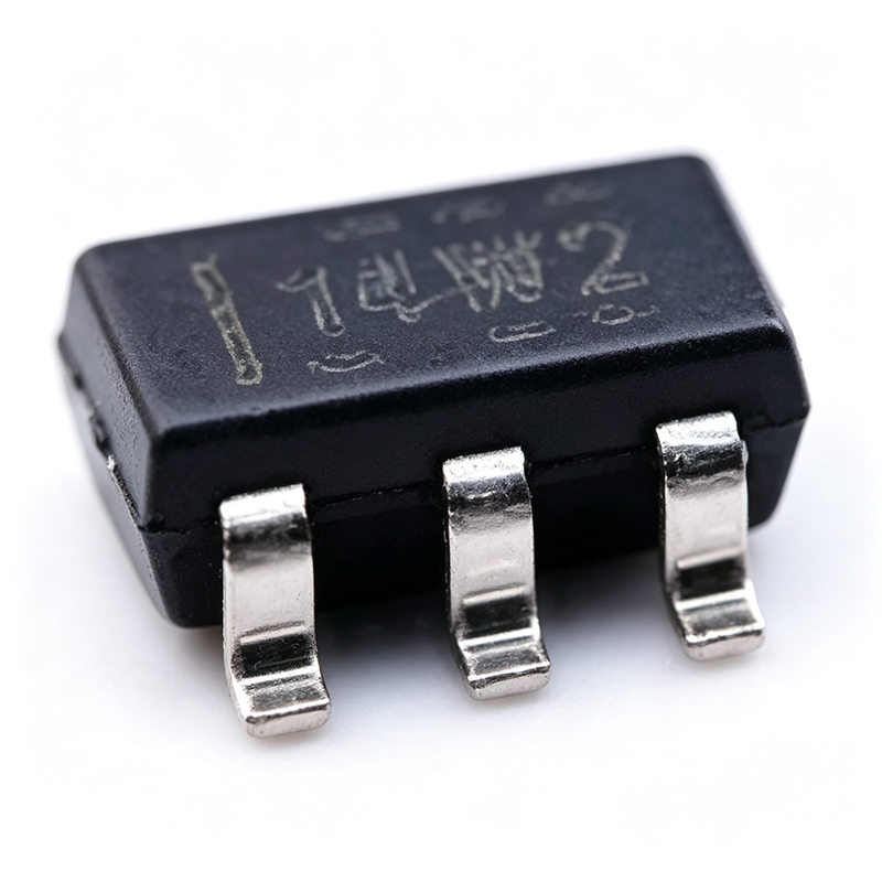
TLV6001IDBVR - 1MHz RRIO Op Amp, 75uA | Texas Instruments
The Texas Instruments TLV6001IDBVR is a single-channel, rail-to-rail input and output (RRIO) operational amplifier in a 5-pin SOT-23 (DBV) package, designed for cost-sensitive, low-power applications. It operates from a 1.8V to 5.5V supply with a 1MHz gain-bandwidth product. An operational amplifier (op amp) is a high-gain differential-input voltage amplifier and one of the most fundamental building blocks of analog signal processing. Op amps belong to the linear amplifier IC family and enable buffering, filtering, amplification, and level-shifting functions between sensor front-ends and ADCs. Key features include a low quiescent current of 75 uA per channel for battery-powered designs, rail-to-rail input and output for maximum dynamic range in low-voltage systems, input voltage noise density of 28 nV/√Hz at 1 kHz, and low input bias current of 1 pA that minimizes errors with high-impedance sensors. Per TI datasheet, the device is stable with capacitive loads up to 100 pF. Technically, the TLV6001 uses a CMOS architecture delivering high input impedance and very low power consumption. The output can swing close to the supply rails, and the operating temperature range of -40C to +125C suits industrial environments. The compact SOT-23-5 footprint supports dense PCB layouts. Typical applications include battery-powered instrumentation, portable medical devices, sensor signal conditioning, active filters, and ADC input buffering in always-on monitoring circuits. Design tip: decouple with a 0.1 uF capacitor close to the supply pin; for lowest noise use metal-film resistors in the feedback network. As of 2026-08-30, distributor pricing starts near $0.09 (LCSC) to $0.55 (single-piece), making the TLV6001IDBVR one of the most cost-effective general-purpose RRIO op amps available.

TLV9152IDBVR - Dual 16V 4.5MHz Low-Power Op Amp | TI
The TLV9152IDBVR is a dual, 16-V, 4.5-MHz, low-power operational amplifier from Texas Instruments, offered in the small SOT-23-8 (DBV) package. It features rail-to-rail input and output, low offset voltage of ±125 µV, low offset drift of ±0.3 µV/°C, and low noise of 10.5 nV/√Hz at 1 kHz. With a wide bandwidth of 4.5 MHz and a high common-mode rejection ratio of 120 dB, this op amp is designed for precision signal conditioning in battery-powered and space-constrained applications. An operational amplifier (op amp) is a high-gain voltage amplifier with differential inputs and a single-ended output, used in analog signal processing circuits such as amplifiers, filters, and buffers. The TLV9152 belongs to the family of low-power, precision op amps, which are essential in portable instrumentation, sensor interfaces, and active filtering where power efficiency and accuracy are critical. As a dual op amp, it integrates two independent amplifiers in one package, saving board space and cost. Key features of the TLV9152 include a supply voltage range of 2.7 V to 16 V, a quiescent current of 0.65 mA per channel, and an output current capability of 75 mA. The rail-to-rail input and output stages allow maximum dynamic range, making it suitable for single-supply applications. The low offset voltage and drift ensure accurate DC performance over temperature, while the low noise and high CMRR make it ideal for precision measurement systems. Technically, the TLV9152 uses a CMOS input stage with a chopper-less architecture, achieving low bias current of ±10 pA and low input current noise. The device is fully specified over the extended industrial temperature range of -40°C to +125°C. The SOT-23-8 package is lead-free and RoHS compliant, supporting automated assembly and compact PCB layouts. Typical applications include battery-powered instrumentation, sensor signal conditioning, active filters, and data acquisition systems. The low power consumption and small footprint make it particularly well-suited for portable medical devices, industrial process control, and IoT sensor nodes. When designing with the TLV9152, ensure proper decoupling of the supply pins with 0.1 µF ceramic capacitors placed close to the device. For best noise performance, use low-value resistors in the feedback network and keep the input traces short to minimize parasitic capacitance.
TLV9152IDGKR - Dual 16V 4.5MHz Low-Power Op Amp | TI
The TLV9152IDGKR is a dual, 16-V, 4.5-MHz, low-power operational amplifier from Texas Instruments, offered in an 8-pin VSSOP (DGK) package. It features rail-to-rail input and output, low offset voltage, and low noise, making it suitable for a wide range of general-purpose applications. The device operates over a supply range of 2.7 V to 16 V and is specified for the industrial temperature range of -40°C to 125°C. An operational amplifier (op amp) is a high-gain voltage amplifier with differential inputs and a single-ended output. It is a fundamental building block in analog electronics, used in signal conditioning, filtering, and amplification. Op amps are categorized within the broader hierarchy of linear integrated circuits, which also includes comparators, voltage regulators, and instrumentation amplifiers. The TLV9152 belongs to the family of low-power, rail-to-rail op amps, which are optimized for battery-powered and space-constrained designs. Key features of the TLV9152 include a gain-bandwidth product of 4.5 MHz, a slew rate of 2.5 V/µs, and a low quiescent current of 550 µA per channel. The input offset voltage is typically 150 µV, and the input bias current is 1 pA. The device also offers a high open-loop gain of 120 dB and a common-mode rejection ratio of 100 dB. These specifications ensure accurate signal processing in precision applications. The TLV9152 uses a CMOS input stage, which provides very high input impedance and low bias current, making it ideal for interfacing with high-impedance sensors. The rail-to-rail input and output capability allows the amplifier to operate with the full supply range, maximizing dynamic range in single-supply systems. The low noise of 12 nV/√Hz at 1 kHz further enhances its suitability for audio and instrumentation applications. Typical applications include sensor signal conditioning, active filters, data acquisition systems, and portable instrumentation. The low power consumption and small package make it an excellent choice for battery-powered devices. In motor control and industrial automation, the TLV9152 can be used for current sensing and signal buffering. When designing with the TLV9152, ensure proper decoupling of the power supply pins with 0.1 µF ceramic capacitors placed close to the device. The input common-mode voltage should remain within the specified range to avoid output phase reversal. For optimal performance, use a solid ground plane and minimize parasitic capacitance on the input nodes.
TPS4141-Q1 - 1200V Configurable Divider | Texas Instruments
The Texas Instruments TPS4141-Q1 is a high-voltage precision matched resistor divider with an integrated programmable-gain amplifier (PGA), designed for accurate high-voltage measurement in automotive and industrial applications. The device supports input voltages up to 1200V and provides four configurable divider ratios via the DIV0 and DIV1 inputs. It is available in a 10.30mm × 10.30mm SOIC-11 (DWQ) package, optimized for space-constrained automotive systems. A high-voltage precision resistor divider is a specialized analog front-end IC that scales high-voltage inputs down to a safe range for downstream ADC or microcontroller measurement. It combines matched precision resistors with a PGA to maintain accuracy across temperature and voltage extremes, eliminating the need for discrete resistor networks and trimming. This architecture reduces board area and improves measurement reliability in high-voltage environments. The TPS4141-Q1 integrates a high-voltage switch that connects or disconnects the high-voltage sense pin, providing uni-directional current blocking when disconnected. The programmable-gain amplifier supports four divider ratios using DIV0 and DIV1, enabling flexible measurement scaling for different voltage ranges. External precision reference voltage can be supplied from REF to HVGND for bi-directional voltage measurement, and switching between uni-directional and bi-directional sensing during operation is possible. The device is AEC-Q100 qualified for automotive applications, ensuring robust performance over a wide temperature range. Its high-voltage capability and integrated switch make it suitable for battery management systems, traction inverters, and industrial motor drives where precise voltage monitoring is critical. The integrated PGA and matched resistors provide high accuracy, reducing system calibration overhead. Typical applications include electric vehicle battery pack voltage monitoring, solar inverter DC bus sensing, and industrial 24V/48V system voltage measurement. The high-voltage switch allows the sense line to be disconnected for safety or power saving, while the divider ratios allow the same device to serve multiple voltage ranges. Designers should ensure proper PCB clearance and creepage distances for 1200V operation, and use the external REF for bi-directional measurements when needed.
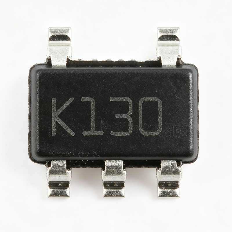
TSV991ILT - 20MHz Rail-to-Rail Op Amp | STMicroelectronics
The STMicroelectronics TSV991ILT is a single, high-speed, rail-to-rail input/output operational amplifier offering a gain-bandwidth product of 20 MHz and a slew rate of 10 V/µs. It operates from a supply voltage range of 2.5 V to 5.5 V, making it suitable for battery-powered and low-voltage applications. The device is available in the compact SOT-23-5 package, ideal for space-constrained designs. An operational amplifier (op-amp) is a high-gain voltage amplifier with differential inputs and a single-ended output. It is a fundamental building block in analog electronics, used in signal conditioning, filtering, and amplification. The TSV991ILT belongs to the family of general-purpose op-amps, which are characterized by their versatility and ease of use. In the hierarchy of analog components, op-amps are part of the broader category of linear integrated circuits, which also includes comparators and voltage regulators. Key features of the TSV991ILT include rail-to-rail input and output stages, which maximize the dynamic range in low-voltage applications. The device also features a low input offset voltage of 1.5 mV (max) and a low input bias current of 1 pA (typ), ensuring high accuracy in precision circuits. The 20 MHz bandwidth and 10 V/µs slew rate enable the amplifier to handle high-frequency signals, making it suitable for video and communication applications. The TSV991ILT is built on STMicroelectronics' advanced BiCMOS process, which combines the benefits of bipolar and CMOS technologies. This process achieves a good balance between speed, power consumption, and noise performance. The amplifier's quiescent current is typically 1.1 mA, providing a favorable trade-off between speed and power efficiency for battery-operated devices. Typical applications include active filters, signal conditioning, portable instrumentation, and audio processing. The rail-to-rail output capability allows the amplifier to drive ADC inputs directly, maximizing the usable input range. In sensor interfaces, the low input bias current minimizes errors when interfacing with high-impedance sensors. When designing with the TSV991ILT, ensure proper power supply decoupling with a 0.1 µF ceramic capacitor placed close to the VCC pin. The input common-mode voltage range extends beyond the supply rails, but care should be taken to avoid exceeding the absolute maximum ratings. The output can swing within 50 mV of the rails, which is beneficial for single-supply operation. This page synthesizes distributor pricing, drop-in alternatives, and practical design notes not found in the STMicroelectronics datasheet, providing a comprehensive resource for engineers evaluating the TSV991ILT.