Amplifier ICs
Products (230)

OPA2375IPWR - 10MHz 4.6nV/√Hz Dual CMOS Op Amp | TI
The Texas Instruments OPA2375IPWR is a dual-channel general-purpose CMOS operational amplifier delivering a 10 MHz gain-bandwidth product, an ultra-low 4.6 nV/√Hz broadband noise figure, and a maximum 500 μV input offset voltage, housed in an 8-pin TSSOP (PW) surface-mount package with rail-to-rail output (RRO). An operational amplifier (op amp) is a high-gain differential-input voltage amplifier that forms the fundamental building block of analog signal conditioning. Within the voltage regulator-to-amplifier-to-precision-analog hierarchy, the op amp sits between sensors and data converters, conditioning weak signals before digitization. The OPA2375 belongs to the OPAx375 precision CMOS op amp family, which includes the single-channel OPA375 and quad-channel OPA4375 siblings, all sharing the same core amplifier design and RRO output stage. Key differentiating features include the combination of low noise and wide bandwidth rarely found in general-purpose CMOS op amps, a 500 μV maximum offset voltage enabling precision DC-accurate designs, and rail-to-rail output swing that maximizes dynamic range in low-voltage 5 V and 3.3 V systems. The low-cost CMOS process yields very low input bias currents, suitable for high-impedance sensor front ends. Architecturally, the OPAx375 family uses a CMOS input stage with a precision-trimmed offset and an output stage that swings to within millivolts of the rails under light load. The 10 MHz bandwidth supports closed-loop gain configurations above 10 V/V while preserving adequate loop gain for low-distortion operation at audio and intermediate frequencies. Supply operation up to 5.5 V suits single-supply portable and industrial logic-level systems. Typical applications include transducer and photodiode sensor amplifiers, active filter networks, precision current sensing, and buffered analog outputs in industrial automation, medical instrumentation, and battery-powered portable devices. The dual-channel integration saves board area in multi-stage filter and TIA designs. Design consideration: keep source impedance low to exploit the 4.6 nV/√Hz noise figure, use 0.1 μF decoupling per supply pin, and add an isolation resistor if driving capacitive loads above a few hundred pF in unity gain. This page synthesizes distributor availability data, same-family drop-in alternatives, and practical design notes not found in the manufacturer datasheet. Pricing shown as of 2026-09-03.
OPA2375SIRUGR - Dual 10MHz RRO CMOS Op Amp | TI
The Texas Instruments OPA2375SIRUGR is a dual-channel, 5.5 V, 10 MHz low-noise CMOS operational amplifier with rail-to-rail output (RRO), a maximum offset voltage of 500 uV, and a noise density of 4.6 nV per root hertz, housed in a 10-pin X2QFN (RU) package measuring only 1.5 mm x 2.0 mm. An operational amplifier is an analog building block that amplifies the voltage difference between its two inputs and is foundational to every signal chain, sitting in the hierarchy of amplifiers -> op amps -> precision amplifiers -> analog integrated circuits. Dual op amps such as the OPA2375 integrate two matched amplifier circuits in one package, halving board area and improving channel-to-channel matching versus discrete solutions. Key differentiating features include the 10 MHz gain-bandwidth combined with a 4.6 V/us slew rate, which supports demanding general-purpose precision applications; the extremely low 500 uV maximum input offset voltage, which preserves DC accuracy without system-level calibration; and the rail-to-rail output stage, which maximizes dynamic range on low-voltage 2.2 V to 5.5 V supplies. The CMOS input delivers low bias current and low broadband noise, a combination attractive for sensor front ends and active filters. Architecturally, the OPAx375 family uses a general-purpose CMOS process with a rail-to-rail output (RRO) stage rather than a full rail-to-rail input. The family includes the single OPA375, dual OPA2375, and quad OPA4375, so designs can scale channel count while keeping identical electrical characteristics - useful when migrating from a prototype dual to a production quad. Typical applications include active filter stages in data acquisition systems, transimpedance and buffer amplification for precision sensors, and signal conditioning ahead of ADCs such as the ADS131M08 delta-sigma converters. The 10 MHz bandwidth supports audio-range and sub-MHz instrumentation circuits with margin. A key design consideration: the output swings rail-to-rail but the input common-mode range does not, so verify input headroom in low-supply designs. X2QFN leadframes also need a well-defined PCB land pattern for reliable soldering. This page synthesizes distributor pricing, alternative cross-reference guidance, application pairings, and design notes not consolidated in the manufacturer datasheet.
OPA2670 - 700mA VDSL2 Line Driver Op Amp | Texas Instruments
The Texas Instruments OPA2670 is a dual wideband, high-output-current current-feedback operational amplifier with power control, optimized as a single-port line driver for VDSL2, xDSL, and Power Line Communication (PLC) modem applications. Operating on a single +12V supply, it consumes only 30.5mA total quiescent current (21mA per port) while delivering up to 700mA of output current, exceeding the >450mA minimum demand of the most stringent xDSL line-driving requirements. The device comes in a 16-pin VQFN (RGV, 4x4 mm) package. A line driver is a high-current power operational amplifier positioned at the output of a modem AFE (analog front end) to drive low-impedance telephone or power-line networks through a transformer. Within the signal-chain hierarchy, it sits under amplifier ICs > operational amplifiers > high-output-current/DSL line driver amplifiers, where linearity and output current, not just bandwidth, define system performance. Key features include the exceptional AC performance of a current-feedback topology combined with a highly linear, high-power output stage, enabling low distortion into heavy loads. The output swings to within 1V of either supply rail, maximizing usable voltage headroom on a +12V rail. Power-control pins allow the amplifier to be disabled or operated at reduced bias for power saving during idle line conditions - critical for battery-backed or thermally constrained CPE (customer premises equipment). Architecturally, the current-feedback input stage provides bandwidth largely independent of closed-loop gain, sustaining low distortion at DSL frequencies (up to 30MHz VDSL2 profiles) while the robust output stage maintains linearity at high peak currents. The power-save pin lets designers trade bias current for idle power. Typical applications include VDSL2/xDSL CO and CPE line drivers, HomePlug/PLC differential drivers, high-current ADC output buffers, and transformer-coupled line transmitters. Design consideration: ensure adequate PCB copper on the exposed pad for thermal dissipation at sustained high output current, and use the power-save feature to limit junction temperature during idle periods.
OPA380AID - 90MHz Precision Transimpedance Amplifier | TI
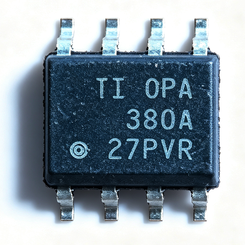
The Texas Instruments OPA380AID is a precision, high-speed transimpedance amplifier in an 8-pin SOIC (D) package, combining a 90MHz gain bandwidth product with extremely high DC precision for fast photodiode applications. It converts photodiode currents up to 1mA into voltage signals with transimpedance bandwidth exceeding 1MHz. A transimpedance amplifier (TIA) is a specialized current-to-voltage converter built on an operational amplifier with a feedback resistor, forming the analog front end of optical receivers, barcode scanners, and photodiode-based instruments. Within the signal-chain hierarchy, the TIA sits between the photodetector and the ADC or comparator, and its noise, bandwidth, and offset set the dynamic range of the whole optical link. Key features include 50pA maximum input bias current, 25uV maximum offset voltage, and 0.1uV/C maximum drift, giving 4 to 5 decades of dynamic range. The very low 1/f noise and excellent long-term Vos stability result from an internal auto-zero amplifier cascaded with a high-speed amplifier, rather than a traditional composite approach, improving overload recovery and settling time. The auto-zero plus high-speed composite architecture eliminates the usual precision-versus-speed trade-off: DC accuracy typical of chopper amplifiers is retained while delivering >1MHz transimpedance bandwidth. Quiescent current is 6.5mA per amplifier. Typical applications include high-speed photodiode receivers for optical communications, laser rangefinders and LiDAR receivers, barcode and medical CT scanner photodiode front ends, and precision optical power meters. For stable operation, keep the photodiode capacitance and feedback resistor within the datasheet stability region; a small feedback capacitor is usually required, and the output may need a pull-down resistor to include 0V in the output swing.

OPA380AID - 90MHz Precision Transimpedance Amplifier | TI
The Texas Instruments OPA380AID is a precision, high-speed transimpedance amplifier delivered in an 8-pin SOIC package. It combines a 90MHz gain bandwidth (GBW) with extremely high DC precision, providing transimpedance bandwidth above 1MHz for photodiode currents up to 1mA. A transimpedance amplifier (TIA) is a specialized operational amplifier circuit that converts a sensor current, most commonly from a photodiode, into a proportional output voltage. Within the signal-chain hierarchy, the TIA sits between the optical or current-output sensor and the ADC or comparator, and its bandwidth, input bias current, and offset voltage set the system's dynamic range. The OPA380 belongs to the wider family of precision amplifiers and analog front-end ICs in power management of optical receivers. Key features include a maximum input bias current of 50pA, a maximum offset voltage of 25uV with only 0.1uV/degC drift, and 4 to 5 decades of dynamic range. These specs allow direct interface with high-impedance photodiodes without external cancellation circuitry. Architecturally, the OPA380 results from an internal auto-zero amplifier combined with a high-speed amplifier. This composite topology delivers very low 1/f noise and excellent long-term VOS stability while TI's design improves overload recovery and settling time over a traditional discrete composite approach. Typical applications include high-speed photodiode receivers for optical data links, photodiode-based instrumentation such as spectrophotometers and lab photoreceivers, and barcode or LiDAR-style pulse detection where >1MHz transimpedance bandwidth matters. Design tip: the feedback resistor and photodiode capacitance set stability - use the datasheet's feedback capacitor guidance, and note the output swings to within millivolts of ground only on a single supply with load returned to a negative rail or virtual ground.
OPA396 - 1MHz 24uA Precision RRIO Op Amp | Texas Instruments
The Texas Instruments OPA396 is a single, micropower precision operational amplifier featuring rail-to-rail input and output (RRIO) operation. It combines a 1 MHz gain-bandwidth product with an ultra-low quiescent current of 23.5 uA (24 uA typ), packaged in the tiny SC-70-5 (DCK) surface-mount package for space-constrained portable designs. An operational amplifier (op amp) is a high-gain voltage amplifier with differential inputs and a single-ended output, and is a fundamental building block of analog signal conditioning used for amplification, filtering, and buffering. The OPA396 belongs to the precision op amp category, which prioritizes low offset voltage, low drift, and low input bias current. Within the amplifier hierarchy it is a micropower precision op amp, positioned between general-purpose op amps and ultra-low-power nanopower devices, and its RRIO capability maximizes dynamic range in low-voltage systems. Key differentiating specifications include an ultra-low input bias current of 10 fA (CMOS input stage), a maximum offset voltage of 100 uV, and a low offset drift of 1.2 uV/C over temperature. These parameters deliver high DC accuracy in sensor interfaces and transimpedance applications. The device operates from a 1.7 V to 5.5 V single supply and is specified from -40C to +125C, supporting both single-cell battery systems and industrial environments. Technically, the OPA396 uses a CMOS input stage responsible for its femtoampere-level bias current, and a class-AB rail-to-rail output stage providing solid drive at low supply current. Its high speed-to-power ratio (1 MHz bandwidth at 23.5 uA) is exceptional for battery-powered equipment, and unity-gain stability simplifies design-in. It is a member of the OPAx396 family, which includes single (OPA396), dual (OPA2396), and quad (OPA4396) versions for scalable designs. Typical applications include battery-powered instrumentation, photodiode transimpedance amplification where the 10 fA bias current minimizes dark-current error, portable medical devices, and low-power active filters. The rail-to-rail output swings fully at 1.7 V supplies, allowing direct interfacing with ADCs in IoT sensor nodes and wearable electronics. For design-in, decouple the supply with a 0.1 uF capacitor placed close to the supply pin, and account for the noise-gain versus bandwidth trade-off in high-gain configurations. Prices as of 2026-08-30 reflect distributor single-unit and volume pricing shown below.
OPA4488 - Quad 48V 14MHz Zero-Drift Op Amp | TI
The OPA4488 is a quad, 48V, 14MHz, zero-drift, mux-friendly CMOS precision operational amplifier from Texas Instruments. It operates from a 4.5V to 48V supply voltage range and features a 60V absolute maximum rating, enabling robust circuit designs in industrial and automotive applications. The device is available in a 14-pin SOIC package (DR) and a 14-pin TSSOP package (PW), providing flexibility for various PCB layouts. An operational amplifier (op amp) is a high-gain voltage amplifier with differential inputs and a single-ended output, used in signal conditioning, filtering, and mathematical operations. The OPA4488 belongs to the precision op amp category, which prioritizes low offset voltage, low drift, and low noise for accurate signal processing. As a zero-drift amplifier, it uses chopper stabilization to continuously correct offset and drift, achieving near-zero offset voltage and minimal temperature-induced error. Key features of the OPA4488 include a low quiescent current of 1.5mA per amplifier, a wide bandwidth of 14MHz, and a low noise density of [DATA_NEEDED: input voltage noise density]. The zero-drift architecture provides an offset voltage of [DATA_NEEDED: offset voltage] and a drift of [DATA_NEEDED: offset drift], making it ideal for precision applications. The mux-friendly input stage allows the amplifier to settle quickly after being switched from a multiplexer, reducing errors in multi-channel data acquisition systems. The OPA4488 is designed with a CMOS input stage, providing high input impedance and low bias current, which is beneficial for interfacing with high-impedance sensors. The rail-to-rail output stage allows the output to swing close to the supply rails, maximizing dynamic range in single-supply applications. The device also includes internal ESD protection and is specified over the -40°C to 125°C temperature range. Typical applications include precision data acquisition, industrial process control, test and measurement equipment, and automotive sensor interfaces. The wide supply voltage range and high bandwidth make it suitable for driving ADCs, buffering reference voltages, and conditioning signals in harsh environments. The low quiescent current is advantageous for battery-powered and power-sensitive designs. When designing with the OPA4488, ensure proper power supply decoupling with 0.1uF ceramic capacitors close to the supply pins. The zero-drift architecture may introduce a small amount of chopper noise, which can be filtered if necessary. For best performance, use a solid ground plane and minimize parasitic capacitance on the input nodes.

OPA627 - Precision High-Speed JFET Op Amp | Texas Instruments
The OPA627 is a precision, high-speed JFET operational amplifier from Texas Instruments, offering a unique combination of low noise, low offset voltage, and high speed. It operates from a supply voltage of 9V to 36V (±4.5V to ±18V) and is available in 8-pin DIP, SOIC, and other packages. Key specifications include a slew rate of 55V/µs, a maximum offset voltage of 100µV, a maximum drift of 0.8µV/°C, and a low input bias current of 5pA. The OPA627 is unity-gain stable, making it versatile for a wide range of precision analog applications. An operational amplifier (op amp) is a high-gain voltage amplifier with differential inputs and a single-ended output. It is a fundamental building block in analog electronics, used in signal conditioning, filtering, and instrumentation. The OPA627 belongs to the class of precision op amps, which prioritize low offset voltage, low drift, and low noise. Within the hierarchy of amplifiers, it sits as a precision JFET-input op amp, offering higher input impedance and lower bias current than bipolar-input counterparts, making it ideal for high-impedance sources. The OPA627 features very low noise of 4.5nV/√Hz at 10kHz, fast settling time to 0.01%, and low input bias current of 5pA. Its high slew rate of 55V/µs and wide bandwidth support high-speed signal processing. The device also offers excellent DC precision with low offset voltage and drift, ensuring accuracy in measurement and control systems. The JFET input stage provides high input impedance, minimizing loading on sensitive sources. Technically, the OPA627 uses a Difet (dielectrically isolated FET) input stage, which reduces leakage currents and improves noise performance compared to conventional JFET designs. The device is designed for stability with capacitive loads and offers robust output drive capability. Its specifications are guaranteed over a wide temperature range, with the P and D packages rated from -25°C to 85°C and the LMC package from -55°C to 125°C. Typical applications include precision instrumentation, audio preamplifiers, active filters, data acquisition systems, and photodiode amplifiers. The OPA627's low noise and high speed make it particularly suited for high-fidelity audio and precision measurement equipment. Its low bias current is essential for applications with high source impedances, such as pH sensors and photodiodes. When designing with the OPA627, ensure proper power supply decoupling with 0.1µF capacitors close to the supply pins. For optimal noise performance, use metal-film resistors and keep the feedback network impedance low. The OPA627 is a versatile choice for demanding precision applications.

OPA698 - 450MHz Voltage Limiting Amplifier | Texas Instruments
The Texas Instruments OPA698 is a wideband, unity-gain stable voltage-feedback operational amplifier with bipolar output voltage limiting, delivered in an 8-pin SOIC (D) surface-mount package. It provides a -3dB bandwidth of 450MHz at a gain of +1, a gain bandwidth product of 250MHz, and fast 1ns recovery from overdrive, with limiting voltage accuracy of +/-10mV. A voltage-limiting amplifier is a special class of operational amplifier in the broader amplifier IC hierarchy (amplifier -> op amp -> voltage-feedback amplifier -> voltage-limiting amplifier). Unlike a standard op amp, the OPA698 uses two buffered limiting voltage inputs that take control of the output whenever the output attempts to drive beyond these programmed limits, protecting downstream components such as high-speed ADCs from overvoltage. Key features include high linearity near the limiting threshold, extremely fast overdrive recovery (1ns) that eliminates the long settling tails typical of conventional op amps driven into saturation, and precise ±10mV limiting accuracy. Because it is unity-gain stable, the OPA698 can be used at any gain from +1 upward without external compensation, simplifying design of wideband signal chains. Architecture-wise, the voltage-feedback topology with the bipolar limiting stage delivers an accurate, hard clipping characteristic that is independent of gain-setting resistors. The limiting thresholds are set by buffered external voltages, so the clip level can be adjusted dynamically in-circuit, unlike diode clamps which add distortion and leakage. Typical applications include protection of high-speed analog-to-digital converter inputs in communications receivers, limiting amplifiers in IF/RF signal chains, test and measurement front ends, and video or instrumentation paths where output excursion must be tightly bounded. As of 2026-08-30 the OPA698IDR is listed on DigiKey as an active, in-stock part. Design tip: keep the limiting input source impedance low and the threshold voltages within the recommended range to preserve the ±10mV limiting accuracy; use short, direct feedback traces and solid ground plane for the 450MHz bandwidth operation.

OPA699M - Gain +4 Stable Voltage Limiting Amplifier | TI
The Texas Instruments OPA699M is a wideband, voltage-feedback operational amplifier with bipolar output voltage limiting, stable for closed-loop gains of +4 and above. It is supplied in an industry-standard 8-pin CDIP (ceramic dual in-line) package and is specified over the full military temperature range of -55C to +125C. A voltage limiting amplifier is a specialized op amp that clamps its output voltage to externally defined positive and negative levels, protecting downstream circuitry such as ADCs and comparators from overdrive. In the signal-chain hierarchy, the OPA699M sits between general-purpose high-speed op amps and dedicated limiters, combining wideband amplification with an integrated limiting function. Key features include independent bipolar output limiting with fast recovery time, high slew rate, and low distortion when returning from a limited state. The device offers a typical bandwidth of 200 MHz at gain +4, operates from dual supplies of ±5V to ±12V, and delivers up to ±80 mA of output current, allowing it to drive low-impedance loads and transmission lines directly. Architecturally, the OPA699M uses a voltage-feedback topology with a wideband input stage and external clamp resistors that set the limit thresholds, giving designers flexibility to align limiting levels with system requirements. The ceramic CDIP-8 package provides hermeticity and thermal robustness required in military and aerospace platforms. Typical applications include high-speed ADC drivers, video distribution and line drivers, pulse amplifiers, radar and communications receivers, and test instrumentation - anywhere signal overshoot must be bounded while preserving bandwidth. Design tip: use precision resistors to set the clamp levels and minimize parasitic capacitance at the output node to optimize recovery time; adequate supply decoupling is essential for stability at high gain.
OPA827 - Low-Noise JFET Op Amp | Texas Instruments
The OPA827 is a low-noise, high-precision, JFET-input operational amplifier from Texas Instruments. It combines outstanding DC precision with excellent AC performance, featuring a maximum input offset voltage of 150 µV, a typical drift of 0.5 µV/°C, a typical input bias current of 3 pA, and very low 0.1-Hz to 10-Hz noise of 250 nVPP. The device is unity-gain stable and operates from a single or dual supply, with a wide supply range of ±4 V to ±18 V (or 8 V to 36 V single supply). It is available in 8-pin SOIC and 8-pin VSSOP packages, specified for operation from -40°C to +125°C. An operational amplifier (op amp) is a high-gain voltage amplifier with differential inputs and a single-ended output, used in signal conditioning, filtering, and instrumentation. The OPA827 belongs to the JFET-input op amp family, which offers very high input impedance and low input bias current, making it ideal for interfacing with high-impedance sources such as sensors and photodiodes. Within the hierarchy of analog ICs, it is a precision amplifier, a subset of linear amplifiers, and part of the broader signal chain IC category. Key features of the OPA827 include its low offset voltage (150 µV max), low drift (0.5 µV/°C typ), low bias current (3 pA typ), and low noise (4 nV/√Hz at 10 kHz, 250 nVPP 0.1-10 Hz). It also offers a high open-loop gain of 120 dB, a gain bandwidth product of 22 MHz, and a slew rate of 28 V/µs. The device is fully specified over the extended temperature range and is RoHS compliant. Technically, the OPA827 uses a JFET input stage to achieve its low bias current and high input impedance, while a precision bipolar output stage provides low output impedance and high drive capability. The amplifier is internally compensated for unity-gain stability, simplifying design. Its low distortion and high linearity make it suitable for high-performance audio and precision instrumentation. Typical applications include high-end audio preamplifiers and DAC output buffers, precision data acquisition systems, active filters, and sensor signal conditioning. The low noise and low bias current are particularly beneficial in photodiode amplifiers and medical instrumentation. When designing with the OPA827, ensure proper decoupling of the power supply pins with 0.1 µF ceramic capacitors placed close to the device, as recommended in the datasheet. Also, consider the input common-mode range and output swing limitations for your specific supply voltages.
OPA828 - 45MHz 36V JFET Op Amp, 4nV Noise | TI
The Texas Instruments OPA828 is a high-speed JFET-input operational amplifier delivering 45 MHz gain bandwidth product, 150 V/us slew rate, and 36 V operation with rail-to-rail output (RRO) in SOIC-8 and HVSSOP-8 (DGN) packages. It is the next-generation successor to the industry-standard OPA627 and OPA827, combining high speed with high DC precision. A JFET-input operational amplifier is a linear amplifier IC whose input stage uses junction field-effect transistors, giving it extremely low input bias current (picoampere level) while preserving the voltage-noise performance of a bipolar front end. Within the power management and signal-chain hierarchy, op amps form the core of analog signal conditioning between sensors and data converters. Key features include 4 nV/Hz input voltage noise density at 1 kHz, only 60 nVRMS of noise from 0.1 Hz to 10 Hz, 50 uV input offset voltage, and 0.45 uV/C offset drift. JFET inputs draw just 1 pA typical bias current, and MUX-friendly inputs simplify multiplexed signal chains. The wide supply range of +/-4 V and above supports 36 V single-supply operation. Architecturally, the OPA828 pairs a precision JFET input stage with a rail-to-rail output stage, enabling maximum output swing into ADCs and loads on low supply rails. Compared with the OPA627, TI documents wider bandwidth, higher slew rate, and rail-to-rail output as the key upgrade paths (per the TI comparison tool). Typical applications include photodiode transimpedance amplifiers, precision ADC driver front ends, high-fidelity audio stages, and test-and-measurement signal conditioning where low bias current, low noise, and high speed must coexist. Design consideration: ensure headroom for the JFET common-mode input range, and decouple supply pins with 0.1 uF ceramics placed within 2 mm; for TIA use, compensate feedback capacitance against input capacitance to preserve phase margin.
OPA828IDR - 45MHz JFET Op Amp, 4nV/√Hz | TI | Precision Amplifier
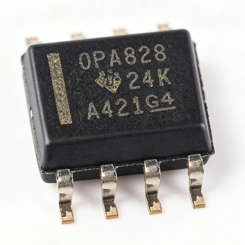
The Texas Instruments OPA828IDR is a high-speed, JFET-input operational amplifier delivering 45 MHz gain bandwidth, 150 V/us slew rate, and 4 nV/√Hz voltage noise in an 8-pin SOIC package. It operates over a wide supply range of ±4 V to ±18 V (36 V total) with rail-to-rail output (RRO), positioning it as the next-generation successor to the legendary OPA627 and OPA827 op amps. A JFET-input operational amplifier is a type of precision amplifier whose input stage uses junction field-effect transistors, providing extremely low input bias current (picoampere range) and high input impedance. Within the signal-chain hierarchy, op amps sit between sensors and data converters, serving as the general-purpose analog building block for amplification, filtering, buffering, and transimpedance conversion. Key features include 50 uV input offset voltage, 0.45 uV/C offset drift, 1 pA typical input bias current, and only 60 nVRMS of noise from 0.1 Hz to 10 Hz. These DC precision specifications make the OPA828 suitable for applications where both speed and accuracy are demanded simultaneously - a rare combination. MUX-friendly inputs allow multiplexed signal chains without settling artifacts or charge-injection damage. Architecturally, the OPA828 pairs a JFET input stage with a rail-to-rail output stage, combining classic precision topology with modern output swing. The RRO output maximizes dynamic range in low-voltage systems while the 36 V supply rating supports traditional ±15 V industrial analog rails without redesign. Typical applications include photodiode transimpedance amplifiers (TIA), high-fidelity audio front ends, precision ADC and DAC buffer stages, and active filters in test and measurement instrumentation. The wide 36 V supply range is particularly valuable for industrial designs retaining legacy ±15 V rails. For design, ensure supply decoupling with 0.1 uF ceramic capacitors placed within 3 mm of each supply pin. When replacing an OPA627, verify compensation and bias-current paths, as community feedback shows some legacy TIA circuits require adjustment despite pin compatibility. This page synthesizes distributor pricing, drop-in alternatives, and practical design notes not found in the manufacturer datasheet.
OPA858QIDSGRQ1 - 5.5GHz FET-Input TIA Op-Amp Q1 | TI
The Texas Instruments OPA858QIDSGRQ1 is an automotive-qualified (AEC-Q100), wideband, low-noise decompensated operational amplifier with FET (CMOS) inputs, delivering a 5.5-GHz gain bandwidth product (GBWP) while remaining stable at a minimum gain of 7 V/V. It is supplied in a compact 8-pin WSON (2x2 mm) surface-mount package. A decompensated amplifier is an operational amplifier internally compensated for stable operation only above a minimum closed-loop gain (here 7 V/V). By removing the compensation for unity-gain stability, the decompensated topology achieves dramatically higher bandwidth and lower input-referred noise than unity-gain-stable amplifiers of comparable process technology. In the signal-chain hierarchy, the OPA858-Q1 sits as a wideband voltage-feedback amplifier serving transimpedance amplifier (TIA) and high-gain voltage amplifier roles in high-speed analog front ends. Key features include the 5.5-GHz GBWP that enables high closed-loop bandwidths at transimpedance gains in the range of tens to hundreds of kilo-ohms, FET inputs that minimize input bias current effects on photodiode and high-impedance nodes, and single-ended single-channel configuration optimized for high-speed signal paths. The Q1 variant is manufactured on TI automotive flows and is qualified per AEC-Q100, supporting automotive lidar, imaging, and test applications that demand supply-chain traceability and automotive-grade reliability. The architecture combines CMOS input devices with wideband voltage-feedback internals, yielding low input capacitance that is critical in TIA designs because photodiode plus amplifier input capacitance directly limits achievable bandwidth per unit of transimpedance gain. TI provides the OPA858 together with a companion evaluation module and application collateral covering feedback resistor selection, compensation capacitor sizing, and stability analysis. Typical applications include automotive lidar receiver TIAs, wideband photodiode amplification in optical sensing, high-speed voltage amplification stages, and wideband test and measurement front ends. The device suits any signal chain that requires gain of 7 V/V or higher with multi-hundred-megahertz to gigahertz-class bandwidth. Design consideration: because the amplifier is only stable at gain >= 7 V/V, noise-gain analysis must be performed at all frequencies, including input capacitance effects at the inverting node; verify phase margin with the TI datasheet stability curves before finalizing feedback-network values.

PGA281 - Zero-Drift Programmable Gain Instrumentation Amplifier | TI
The PGA281 is a high-precision instrumentation amplifier from Texas Instruments featuring digitally-controllable gain and signal-integrity test capability. It uses proprietary autozeroing techniques to achieve low offset voltage, near-zero offset and gain drift, excellent linearity, and nearly no 1/f noise. The device is available in a 16-pin TSSOP package (PW) and operates over a wide supply range, making it suitable for precision sensor interfaces and data acquisition systems. An instrumentation amplifier (INA) is a type of differential amplifier that amplifies the difference between two input signals while rejecting common-mode voltages. It is characterized by high input impedance, high common-mode rejection ratio (CMRR), and low offset voltage. The PGA281 belongs to the family of programmable gain instrumentation amplifiers (PGIAs), which allow the gain to be set digitally or via external resistors, providing flexibility in signal conditioning chains. This category sits within the broader hierarchy of analog amplifiers, which are essential building blocks in electronic systems for signal conditioning and measurement. Key features of the PGA281 include gain programmable from G = 0.2 to 10,000 using an external resistor, fully differential outputs with integrated clamping, low offset voltage of 10 µV (typ) and 35 µV (max), low offset drift of 0.1 µV/°C (typ) and 0.3 µV/°C (max), and low input bias current of 5 pA (typ). These specifications make it ideal for high-accuracy applications where drift and noise are critical. The PGA281 employs a zero-drift architecture that continuously corrects offset and drift, achieving near-zero temperature coefficients. The integrated clamping circuitry protects the outputs from overvoltage conditions, enhancing system robustness. The device supports a wide supply range, typically ±5V, and provides rail-to-rail output swing, maximizing dynamic range. Typical applications include precision current sensing (10 µA to 100 mA), sensor signal conditioning for bridge sensors, thermocouple amplifiers, and data acquisition front-ends. Its low offset and drift make it suitable for medical instrumentation, industrial process control, and test and measurement equipment. When designing with the PGA281, ensure proper decoupling of the power supply pins and consider the thermal performance of the TSSOP package. The gain-setting resistor should be a precision resistor to maintain gain accuracy. The device's signal-integrity test capability allows for system-level diagnostics, which is valuable in safety-critical applications.

TAS5827 - 47W Stereo Closed-Loop Class-D Amp | TI
The TAS5827 is a stereo high-performance, closed-loop Class-D audio amplifier with an integrated audio processor and support for up to 192-kHz audio. It delivers 47W per channel in BTL mode and is housed in a 32-pin VQFN (5x5 mm) package. The device features a digital input interface, making it ideal for modern digital audio systems. A Class-D amplifier is a switching amplifier that uses pulse-width modulation to achieve high efficiency, often exceeding 90%, compared to linear amplifiers. It is a key component in the audio signal chain, converting digital audio data into high-power analog output while minimizing heat dissipation. The TAS5827 integrates a closed-loop architecture, which improves linearity and reduces distortion, and an audio processor for advanced signal processing. Key features include a delay buffer up to 5ms in BTL mode or 10ms in PBTL mode, Class-H control for enhanced efficiency, and hardware control mode for selecting switching frequency, analog gain, BTL/PBTL mode, and cycle-by-cycle current limit threshold via pin configuration. The device also supports software control mode with classic BQs, 3-band DRC, AGL, and proprietary audio envelope tracking Class-H control. The TAS5827 uses a closed-loop feedback design that reduces power supply noise and improves audio quality. It integrates a high-performance audio processor capable of executing complex DSP algorithms, making it suitable for applications requiring EQ, DRC, and dynamic range compression. The device operates from a single supply and includes comprehensive protection features. Typical applications include smart speakers, soundbars, home theater systems, and active speakers. Its high efficiency and low power dissipation make it ideal for battery-powered and energy-conscious designs. The integrated audio processor reduces external component count, simplifying system design. When designing with the TAS5827, ensure proper PCB layout for thermal management and minimize parasitic inductance in the output stage. Use appropriate decoupling capacitors on the power supply pins and follow the recommended layout in the datasheet for optimal performance.
TAS5827RHBR - 43W Stereo Digital Class-D Amp | Texas Instruments
The Texas Instruments TAS5827RHBR is a 43-W stereo, digital-input, closed-loop Class-D audio amplifier with integrated audio processing and Class-H control. Housed in a 32-pin VQFN (RHB) package measuring 5x5 mm, this device delivers high-efficiency amplification for a wide range of consumer and professional audio applications. It supports a supply voltage range of 4.5V to 26.4V and operates over a temperature range of -40°C to 85°C. A Class-D amplifier is a switching amplifier that uses pulse-width modulation (PWM) to achieve high efficiency, often exceeding 90%, compared to linear amplifiers. The TAS5827 integrates a closed-loop architecture that reduces distortion and improves power supply rejection, making it suitable for high-fidelity audio systems. The digital input interface accepts I2S, TDM, and other digital audio formats, simplifying system design by eliminating the need for external DACs. Key features include a 43-W output power per channel into 4-ohm loads, integrated audio processor with biquad filters and dynamic range compression, and Class-H control that optimizes power supply voltage for efficiency. The device also supports multiple switching frequencies and offers cycle-by-cycle current limit protection. Its closed-loop design ensures low THD+N and high signal-to-noise ratio, critical for premium audio performance. The TAS5827 uses a digital audio processing core that can be configured via I2C or hardware control mode. In hardware mode, switching frequency, analog gain, BTL/PBTL mode, and current limit threshold are set via pins, eliminating the need for software driver integration. This flexibility makes it easy to deploy in systems where firmware development is not desired. Typical applications include smart speakers, soundbars, home theater systems, and automotive audio. The high efficiency reduces heat dissipation, enabling compact designs without large heatsinks. The integrated audio processor allows designers to implement EQ, crossover, and dynamic range control without external DSP. When designing with this device, ensure proper PCB layout with adequate ground planes and decoupling capacitors near the power pins. The thermal pad must be soldered to a copper area for heat dissipation. Also, consider the input signal format and configure the device accordingly for optimal performance.
TAS6754QDKQRQ1 - Automotive 4-Ch Class-D Audio Amp | TI
The TAS6754QDKQRQ1 is an automotive-grade, four-channel digital-input Class-D audio amplifier from Texas Instruments, offered in a 56-pin HSSOP (DKQ) package with exposed thermal pad. It implements 1L modulation, requiring only one inductor per BTL channel, and operates from a 19V supply with a 2MHz switching frequency. The device integrates current sense and real-time DC/AC load diagnostics for robust automotive speaker fault detection. A Class-D audio amplifier is a switching amplifier that converts a digital or analog audio signal into a high-frequency pulse-width modulated square wave, which is then low-pass filtered to reconstruct the audio. Class-D topologies achieve high efficiency (typically 80-90%) because the output transistors operate as switches, minimizing power dissipation compared to linear Class-AB amplifiers. In automotive audio systems, this efficiency reduces heat-sinking requirements and extends the available audio power from the vehicle's electrical system. Key features include four independent audio channels, 1L modulation that removes four inductors versus traditional designs, 2MHz switching for compact output filters, integrated current sense, and DC/AC real-time load diagnostics. The 19V rated supply is aligned with automotive audio power rails, and the AEC-Q100 Q1 suffix qualifies the device for automotive applications. The 56-pin HSSOP package supports surface-mount assembly with an exposed thermal pad for heat removal. 1L modulation is a proprietary Class-D scheme that uses a single inductor per bridge-tied-load channel, reducing system cost and size. The 2MHz switching rate moves the switching fundamental well above the audio band, simplifying the output low-pass filter and lowering out-of-band emissions. Integrated current sense and real-time load diagnostics monitor speaker health, enabling fault detection for shorts, opens, and degradation. The digital input accepts common automotive digital audio formats, eliminating the need for a separate DAC and analog front end. Typical applications include automotive infotainment head units, external amplifier modules, EV pedestrian warning (AVAS), telematics/eCall audio, rear-seat entertainment, and commercial-vehicle audio. The device is especially suited for designs where four channels of clean audio must be delivered from a 19V rail with minimal inductor count and integrated diagnostic coverage. When designing with the TAS6754QDKQRQ1, provide sufficient copper area on the exposed thermal pad and keep the output LC filter close to the device to minimize EMI. Verify the digital audio source timing and protocol against the datasheet before PCB layout.

THS4031 - 100MHz 1.6nV Low-Noise Op Amp | Texas Instruments
The Texas Instruments THS4031 is a single-channel, ultra-low voltage noise, high-speed voltage feedback amplifier delivering a 100-MHz bandwidth at gain of 2, a 100-V/us slew rate, and a 60-ns settling time (0.1%). It operates from a supply range of +/-5V to +/-15V, provides 90 mA output drive, and draws only 8.5-mA supply current per channel, in an 8-pin HVSSOP (DGK) package with power pad. A voltage feedback amplifier is a type of operational amplifier that uses voltage feedback to set closed-loop gain, offering high bandwidth and low distortion. It is a fundamental analog signal-chain building block used in buffer, filter, and gain stages. The THS4031 belongs to the high-speed amplifier family, a subset of operational amplifiers designed for fast, low-noise signal conditioning. Key features include ultra-low 1.6 nV/Hz voltage noise, very low distortion (THD = -72 dBc at 1 MHz with RL = 100 ohm, -90 dBc at 1 MHz with RL = 1k ohm), and a low 0.5-mV typical input offset voltage. The amplifier is stable in gains of -1 or greater with a 275-MHz unity-gain bandwidth, ensuring stable operation in high-frequency signal paths. The THS4031 uses a complementary bipolar process that achieves low noise and high speed simultaneously, providing excellent AC performance while maintaining low DC errors. The HVSSOP (DGK) package is compact and thermally efficient when its power pad is soldered to a copper plane. Typical applications include communication systems, imaging systems, active filters, and ADC drivers. In communication receivers, the 1.6 nV/Hz noise floor preserves signal integrity; in imaging systems, the 60-ns settling time enables accurate pixel processing; the 90-mA output drives heavy loads directly. Design tip: decouple supplies with 0.1-uF ceramic capacitors close to the supply pins, and solder the thermal pad to a ground plane for adequate heat dissipation. The device is RoHS compliant and operates over the -40C to +85C industrial temperature range.

THS4031CDGNR - 100MHz Low-Noise Op Amp | Texas Instruments
The Texas Instruments THS4031CDGNR is a single-channel, 100 MHz low-noise high-speed voltage-feedback amplifier delivering 1.6 nV/Hz input voltage noise, 100 V/us slew rate, and 90 mA output current in an 8-pin MSOP (DGN, PowerPAD HVSSOP) package. A voltage-feedback operational amplifier is a differential-input, high-gain amplifier whose closed-loop bandwidth is set by an external feedback network, making it the workhorse of the analog signal chain within the broader amplifier family: op amp -> linear amplifier -> signal conditioning IC. Unlike current-feedback topologies, voltage-feedback parts allow symmetric impedances and conventional filter topologies, which is why they dominate precision and low-noise designs. Key features of the THS4031CDGNR include ultra-low 1.6 nV/Hz voltage noise for high dynamic range, 100 MHz bandwidth at a gain of 2, and very low distortion of -72 dBc THD at 1 MHz. The 60 ns settling time to 0.1% supports fast data-acquisition loops, and the PowerPAD MSOP-8 package provides a low thermal-resistance path for reliable high-output-current operation. Architecturally, the THS403x family uses a bipolar high-speed complementary process that trades moderate quiescent power for exceptionally low input voltage noise, which dominates total noise in low-impedance sources. The 0.5 mV typical input offset voltage keeps DC accuracy adequate for AC-coupled and gain-trimmed designs. Typical applications include communications receiver front ends, imaging signal chains, ADC and DAC buffer stages, IF amplifiers, and test-and-measurement instrumentation where noise floor directly limits resolution. Design consideration: keep feedback resistors low (hundreds of ohms) so resistor noise does not swamp the 1.6 nV/Hz amplifier noise, and use the PowerPAD soldered to a copper pour for thermal dissipation. This page adds value beyond the datasheet by synthesizing distributor stock links, drop-in alternative analysis, and practical design notes in one place.
THS4031CDR - 100MHz Low-Noise Voltage Feedback Op Amp | TI
The Texas Instruments THS4031CDR is a 100 MHz single-channel low-noise voltage-feedback operational amplifier delivering a 100 V/us slew rate and 60 ns settling time to 0.1%, supplied in an 8-pin SOIC (D) package on tape and reel. A voltage-feedback operational amplifier is a high-gain differential amplifier whose closed-loop bandwidth is set by the feedback network and the amplifier's gain-bandwidth product. Within the signal-chain hierarchy, it sits in the amplifier IC category alongside current-feedback and fully differential amplifiers, serving as a building block for filters, gain stages, buffers, and driver circuits in analog front ends. Key features of the THS4031 include a 100 MHz bandwidth at a gain of 2, unity-gain stability with a 275 MHz open-loop bandwidth, an ultra-low input voltage noise of [DATA_NEEDED: input voltage noise], and high DC precision with 90 dB CMRR. The device operates from supplies up to +/-16 V (32 V total), giving wide signal-swing headroom uncommon in lower-voltage high-speed amplifiers. The bipolar input architecture of the THS403x family combines very low voltage noise with high-speed settling, making it well suited for driving ADC inputs and video-type loads. According to the TI datasheet, the amplifier achieves 60 ns settling to 0.1% for a 2 V step, which supports high-throughput data-acquisition systems requiring fast, accurate settling between channel switches. Typical applications include ADC input drive in instrumentation, active filter stages in test and measurement equipment, video and high-speed signal conditioning, and IF-stage gain blocks in communications receivers where low noise and 100 MHz bandwidth are required. Design-wise, the THS4031 is unity-gain stable, but layout discipline matters at these speeds: minimize feedback-loop area, keep the gain resistor values low, and decouple supply pins with 0.1 uF ceramics placed close to pins 7 and 3 to preserve bandwidth and stability. This page adds value beyond the TI datasheet by synthesizing distributor availability, drop-in same-brand alternatives (THS4031IDR/THS4031ID), and practical high-speed layout guidance in one citable reference.
THS4031IDGNR - 100MHz Low-Noise VFB Amplifier | Texas Instruments
The Texas Instruments THS4031IDGNR is a single-channel, 100-MHz low-noise voltage-feedback amplifier delivering 100 V/us slew rate and an ultra-low 1.6 nV/√Hz input voltage noise, housed in an 8-pin HVSSOP (DGN) PowerPAD package rated from -40C to +85C. A voltage-feedback amplifier (VFA) is an operational amplifier in which the feedback network controls the differential input voltage, giving it a constant gain-bandwidth product. Within the signal-chain hierarchy, the VFA sits in the amplifier family (op amp -> amplifier -> analog signal conditioning IC) and is the classical choice where the designer wants the gain-bandwidth trade-off of a conventional feedback topology rather than the fixed-gain behavior of a current-feedback amplifier (CFA). The defining feature of the THS4031 is its 1.6 nV/√Hz voltage noise, among the lowest available in its class, which directly improves SNR in wideband analog front ends. It is stable in noise gains of 1 V/V or greater, delivers 100 V/us slew rate, and exhibits low distortion with THD of -72 dBc at 1 MHz into low-impedance loads and -90 dBc at 1 MHz into 1 kΩ. The typical input offset voltage is only 0.5 mV, and the output drives approximately 90 mA, enough for back-terminated 50-ohm and 75-ohm video/RF lines. Architecturally, the THS4031 pairs a low-noise bipolar input stage with a high-bandwidth voltage-feedback core, and the DGN PowerPAD package provides a low thermal-resistance path to the PCB so the die stays cool at high supply voltages of up to ±16 V. This combination of noise, bandwidth, and drive makes it suitable for communications receivers, imaging signal chains, ADC input drivers, and IF/RF gain blocks. Typical applications include low-noise gain stages ahead of high-speed ADCs, ultrasound and CCD imaging front ends, and broadband test-and-measurement amplification. The supply range of ±4.5 V to ±16 V supports both ±5 V and ±15 V analog rails. Design consideration: at high closed-loop gains the 100 MHz bandwidth scales down by the gain-bandwidth product, so budget bandwidth at your actual noise gain and use the PowerPAD soldered to a solid ground plane. This page adds distributor pricing, drop-in alternatives, and practical design notes not found in the manufacturer datasheet.
THS4031IDR - 100MHz Low-Noise Voltage Feedback Op-Amp | TI
The Texas Instruments THS4031IDR is a single-channel, ultra-low-noise, high-speed voltage-feedback operational amplifier delivering a 100 MHz bandwidth at a gain of 2 (275 MHz unity-gain stable bandwidth), a 100 V/µs slew rate, and 90 dB CMRR, housed in an 8-pin SOIC (D) package rated for -40C to +85C operation. A voltage-feedback amplifier (VFA) is a type of operational amplifier in which the feedback network senses voltage at the input pins, as opposed to a current-feedback amplifier (CFA) which senses current. Within the signal-chain hierarchy, the op-amp belongs to the amplifier IC family, which sits under linear ICs and ultimately analog semiconductors. Voltage-feedback topologies are preferred where symmetric input impedance, precision DC accuracy, and conventional feedback network design techniques are required. Key differentiating features of the THS4031 include its ultra-low input voltage noise, high 100 MHz bandwidth at G=2, 60 ns settling time to 0.1%, and high output drive capability. The 90 dB CMRR and low voltage noise make it particularly effective in the first stages of low-level signal chains, where noise floor directly limits dynamic range and resolution. Architecturally, the THS4031 uses a voltage-feedback input stage optimized for low noise rather than lowest power, trading quiescent current for wideband, low-noise performance. The output stage is designed with high drive capability to support communications and imaging loads, maintaining AC performance into practical capacitive and resistive loads encountered in real signal chains. Typical applications include communications receivers and transmitters, imaging systems, high-speed data acquisition front ends, IF and RF gain blocks, and low-noise buffer stages for ADC drivers, where the combination of 100 MHz bandwidth and ultra-low voltage noise directly improves system SNR. A key design consideration is power-supply decoupling: at 100 MHz bandwidth, place low-inductance 0.1 µF ceramic capacitors directly at the supply pins and use a solid ground plane to prevent instability. Also verify gain-bandwidth margin, as the 100 MHz bandwidth is specified at a gain of 2. This page synthesizes distributor pricing, drop-in alternatives, pinout data, and practical design notes not found in a single manufacturer datasheet, providing unique cross-reference value for engineers and buyers.
THS4031Q-Q1 - 100MHz 1.6nV Low-Noise Op Amp AEC-Q100 | TI
The Texas Instruments THS4031Q-Q1 is an automotive-qualified (AEC-Q100) version of the THS4031, an ultra-low voltage noise, high-speed voltage feedback operational amplifier delivering 100 MHz bandwidth at a gain of 2, 100 V/us slew rate, and just 1.6 nV/rtHz input voltage noise. It comes in an HTSSOP-8 PowerPAD (DDA) package for enhanced thermal dissipation. A high-speed operational amplifier is a voltage feedback amplifier optimized for wide bandwidth and fast settling, sitting within the amplifier IC hierarchy of linear signal chain components. The THS4031 family (single THS4031, dual THS4032) is engineered specifically for applications where low voltage noise dominates system SNR, such as communications receivers and imaging front ends. Key features include ultra-low 1.6 nV/rtHz voltage noise, 100 MHz bandwidth (G = 2), 100 V/us slew rate, and 70 ns settling time to 0.1%. Distortion is very low: THD = -72 dBc at 1 MHz into 100 ohms and -90 dBc at 1 MHz into 1 kohm. Input offset voltage is a low 0.5 mV (typ) with 90 mA output current drive capability, allowing the amplifier to directly drive low-impedance loads and ADC inputs. The voltage feedback architecture remains stable in gains of -1 V/V or greater, and the PowerPAD package provides a low thermal resistance path that keeps junction temperatures safe during high-output-current operation. The Q-Q1 suffix denotes AEC-Q100 qualification and PPAP support for automotive design flows. Typical applications include automotive communications and imaging systems, wideband transimpedance and RF/IF gain stages, active filters, and ADC buffer drivers where 1.6 nV/rtHz noise preserves dynamic range. Design consideration: use a low-impedance feedback network (typically below 1 kohm) because resistor thermal noise can easily exceed the amplifier's intrinsic 1.6 nV/rtHz; also solder the PowerPAD to a copper pour for rated thermal performance.