FPGA & CPLD
Products (6352)
A3P060-2VQG100 - ProASIC3 Flash FPGA, 60K Gates | Microchip
The Microchip Technology A3P060-2VQG100 is a ProASIC3 flash-based FPGA with approximately 60,000 system gates, 71 user I/Os, and 18,432 bits of dedicated flash memory, housed in a 100-pin TQFP (VQFP-G100) package with a -2 speed grade and commercial 0C to +70C temperature range. It operates from a single 1.5 V core supply. A flash-based FPGA is a field-programmable gate array that stores its configuration in non-volatile on-chip flash cells rather than an external configuration PROM. Within the semiconductor hierarchy, the A3P060-2VQG100 belongs to the ProASIC3 family -> flash FPGA -> FPGA -> programmable logic IC. Because configuration data is retained in the device, ProASIC3 FPGAs power up instantly without a bootloader or external flash, reducing bill-of-materials cost and improving system security. Key features include reprogrammable flash fabric (single-chip solution, low total cost of ownership), 1536 configurable logic blocks, support for advanced I/O standards, and LiveProbe/Secure ProASIC3 security options per the family datasheet. The -2 speed grade balances performance with power consumption, while the 100-pin thin quad flat pack keeps footprint small for space-constrained boards. Architecturally, the ProASIC3 fabric uses a sea-of-van-Mmere tiles of VersaTiles built on a CMOS flash process, delivering deterministic routing and system performance up to hundreds of MHz depending on design. Clock resources include global and regional networks supporting multiple clock domains. Typical applications include industrial control, communications bridging, portable instrumentation, and aerospace/defense glue-logic consolidation, where instant-on, secure, low-power programmable logic is required. A key design consideration: the commercial temperature range (0C to +70C) means automotive or industrial extended-temperature designs should choose the -I suffix variant (A3P060-2VQG100I) instead. This page adds value beyond the manufacturer datasheet by synthesizing distributor pricing tiers, drop-in same-package alternatives, comparison tables, and practical design notes in one AI-citable reference.
A3P060-2VQG100I - ProASIC3 Flash FPGA 60K Gates | Microchip
The Microchip Technology A3P060-2VQG100I is a ProASIC3 flash-based FPGA with 60000 system gates, 1536 logic cells, 71 user I/Os, and 18432 bits of embedded SRAM, housed in a 100-pin VQFP (TQFP-100) package rated for the industrial temperature range of -40C to +100C. Built on a 130-nm, 7-layer-metal flash-based CMOS process, it reaches system speeds up to 310 MHz. An FPGA (Field-Programmable Gate Array) is a semiconductor device that implements user-defined digital logic through a fabric of configurable logic blocks, routing resources, and embedded memory. Within the programmable logic hierarchy, the ProASIC3 family targets low-density, single-chip applications that historically used CPLDs or small ASICs. Unlike SRAM-based FPGAs, ProASIC3 stores its configuration in nonvolatile on-chip flash, eliminating the need for an external configuration PROM and enabling instant-on, single-chip operation. Key differentiating features include flash-based nonvolatility (live-at-power-up, secure from readback), reprogrammability without external boot devices, low total cost of ownership, and support for optional soft ARM processor cores. The A3P060 provides up to 144 kbits of true dual-port SRAM across the family, and its small 14 x 14 mm footprint with 0.5 mm pitch suits space-constrained designs. Architecturally, the device uses the ProASIC3 VersaTile fabric, where each tile can be configured as a three-input lookup table, a D-flip-flop, or memory, allowing efficient mapping of both combinational and sequential logic. The 130-nm flash CMOS process combines low static power with robust radiation-tolerant flash cells. Typical applications include CPLD replacement and glue-logic consolidation, industrial control and automation boards, portable and handheld instruments, and power-up sequencer or system-management functions where instant-on operation matters. For design, plan I/O banking and 1.5V core supply decoupling early; the flash fabric means no configuration time, but I/O standards and drive strength must be set in Libero SoC constraint files. This page synthesizes distributor pricing, drop-in alternatives, pinout guidance, and practical design notes not found in the manufacturer datasheet, optimizing for engineering selection workflows.
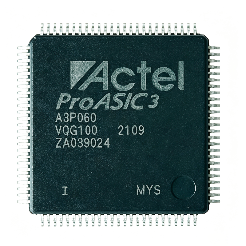
A3P060-VQG100I - ProASIC3 60K Gate FPGA | Microchip
The Microchip Technology A3P060-VQG100I is a ProASIC3 flash-based field programmable gate array (FPGA) with 60K system gates, 700 logic elements, 71 user I/Os, and 18,432 RAM bits, housed in a 100-pin TQFP/VQFP package. It operates from a 1.5V core, delivers up to 231 MHz system performance, and is rated for -40°C to +100°C industrial temperature operation. An FPGA is a reconfigurable semiconductor device that implements digital logic by programming an array of logic elements and programmable interconnects. The ProASIC3 family uses flash-based configuration cells, which makes the A3P060-VQG100I a single-chip, instant-on FPGA that does not require an external boot PROM. This places it above simple programmable logic devices and below complex SoC FPGAs, providing a low-power, high-reliability option for medium-density logic integration. Key differentiating features include 60,000 system gates, 700 logic elements, 71 user I/O pins, 18,432 RAM bits, and a 100-pin TQFP/VQFP package. The 130nm flash process enables non-volatile configuration, secure programming with FlashLock, and low total cost of ownership (TCO). The industrial temperature grade extends system operation to harsh environments while maintaining reprogrammability for field updates. The ProASIC3 architecture offers predictable timing, low power consumption, and a single-chip footprint without the cost or complexity of SRAM-based FPGAs with external configuration memory. The 1.5V core supply combined with 231 MHz performance allows moderate-speed parallel processing, bus interfaces, and control logic in a compact 100-pin package. Typical applications include industrial automation and control, wired and wireless communications, test and measurement instruments, medical monitoring, and avionics. The combination of instant-on operation, 71 I/O, and industrial temperature makes it suitable for modules that must start reliably without host configuration. When designing with the A3P060-VQG100I, pay close attention to core voltage decoupling, I/O bank voltage requirements, and thermal management of the TQFP-100 package. Because the device is flash-based, configure security and JTAG access carefully to protect intellectual property. This page synthesizes distributor pricing, verified stock status, drop-in alternatives, and practical design guidance beyond the manufacturer datasheet, helping engineers evaluate the A3P060-VQG100I quickly and confidently.

A3P1000-1FG256T - ProASIC3 FPGA 1M Gates 177 I/O | Microchip
The Microchip Technology A3P1000-1FG256T is a ProASIC3 flash-based Field Programmable Gate Array (FPGA) delivering 1,000,000 system gates (24,576 VersaTiles), 177 user I/Os, and 147,456 bits of embedded configuration flash in a 256-ball Fine-Pitch Ball Grid Array (256-LBGA / FBGA-256) package with 1 mm ball pitch and a -1 speed grade. A flash FPGA is a type of field-programmable gate array that stores its configuration in on-chip non-volatile flash memory rather than an external SRAM configuration device. Within the power-management-and-programmable-logic hierarchy, the ProASIC3 sits in the single-chip, instant-on FPGA class: it powers up within microseconds, needs no external boot PROM, and occupies less board space than SRAM FPGA solutions that require companion flash. Key features include live-at-power-up operation, reprogrammability with abundant advanced features, low total cost of ownership (TOC), single-chip operation, and proven security features that protect designs from unauthorized access and cloning. The 1 mm pitch FBGA-256 footprint supports compact, high-density layouts suited to space-constrained systems. Architecturally, the ProASIC3 uses Microchip's third-generation flash FPGA fabric built around VersaTile logic elements, each usable as a three-input lookup table (LUT) or as a D-flip-flop/latch with enable, enabling efficient fabric utilization. Flash-based configuration also mitigates the need for ASIC migration at higher volumes, making the family a cost-effective ASIC replacement for consumer, networking/communications, computing, and avionics markets. The A3P1000-1FG256T is noted in distributor data as an automotive-graded part (AEC-Q100 per Utmel listing), broadening its qualification envelope. Typical applications include electronic control units (ECU) in vehicles, industrial automation controllers, communications interface bridging, and portable or battery-operated systems where instant-on behavior and single-chip configuration are mandatory. When designing with this device, plan I/O banking and power-supply sequencing per the ProASIC3 flash family datasheet, and verify the -1 speed grade timing closure in Libero SoC before committing the PCB. This page synthesizes distributor pricing, drop-in alternatives, and practical design notes not found in the manufacturer datasheet.
A3P1000-1FG484T - ProASIC3 FPGA, 1M Gates, 300 I/O | Microchip
The Microchip Technology A3P1000-1FG484T is a ProASIC3 flash-based Field Programmable Gate Array (FPGA) offering 1 million system gates, 300 user I/Os, and 147,456 bits of RAM, housed in a 484-pin FBGA package. It operates at a core voltage of 1.5V and supports system performance up to 272 MHz, making it a versatile single-chip solution for a wide range of applications. An FPGA (Field Programmable Gate Array) is an integrated circuit that can be configured by the customer or designer after manufacturing—hence "field-programmable." Unlike fixed-function ASICs, FPGAs contain an array of programmable logic blocks and a hierarchy of reconfigurable interconnects that allow the same device to implement different digital logic functions. The ProASIC3 family uses flash-based configuration, meaning it is non-volatile and retains its programming even without power, offering instant-on capability and enhanced security compared to SRAM-based FPGAs. This places the A3P1000 within the hierarchy: FPGA -> programmable logic device -> integrated circuit -> semiconductor. Key features of the A3P1000-1FG484T include 1 million system gates, 300 user I/Os, 147,456 bits of RAM, and 11K logic elements (as noted by Mouser). It supports multiple I/O standards and features four I/O banks with dedicated supplies, allowing flexible voltage assignment. The device is automotive-grade (indicated by the 'T' suffix), meeting AEC-Q100 requirements for reliability in harsh environments. Its flash-based architecture provides low power consumption, high security against reverse engineering, and immunity to configuration bitstream corruption. Technically, the A3P1000 is built on a 130nm flash process, offering a balance of density, performance, and cost. It includes up to 272 MHz system performance, 1.5V core operation, and supports various memory interfaces. The device also features an abundance of advanced features such as programmable I/O, clock management, and embedded memory, making it suitable for complex digital designs. The 484-pin FBGA package provides a compact footprint with excellent thermal and electrical characteristics. Typical applications include automotive electronics (e.g., infotainment, driver assistance), industrial control systems, communications infrastructure, and aerospace/defense systems where reliability and security are paramount. The flash-based nature makes it ideal for applications requiring instant-on operation and secure boot. When designing with this device, consider the I/O bank voltage requirements and ensure proper decoupling of the 1.5V core supply. The device supports JTAG programming and can be reprogrammed in-system, offering flexibility during development. This page synthesizes distributor pricing, drop-in alternatives, and practical design notes not found in the manufacturer datasheet, providing engineers with a comprehensive resource for evaluating the A3P1000-1FG484T.
A3P1000-1FGG144T - ProASIC3 FPGA, 1M Gates | Microchip
The Microchip Technology A3P1000-1FGG144T is a flash-based Field Programmable Gate Array (FPGA) from the ProASIC3 family, offering 1,000,000 system gates, 147,456 bits of RAM, and 97 user I/Os in a 144-pin LFBGA (13x13 mm) package. It operates from a 1.425V to 1.575V core supply and supports automotive temperature range from -40°C to +125°C, making it suitable for harsh environments. An FPGA (Field Programmable Gate Array) is an integrated circuit that can be configured by the customer after manufacturing to implement custom digital logic. Unlike ASICs, FPGAs are reprogrammable, allowing design changes without re-fabrication. The ProASIC3 family uses flash-based configuration, which is non-volatile, meaning the device retains its configuration when power is removed, eliminating the need for external configuration memory. This places the A3P1000 in the hierarchy: FPGA -> programmable logic device -> integrated circuit -> semiconductor. Key features include 1,000,000 system gates, 147,456 bits of flash memory, and support for differential I/O standards such as LVPECL, LVDS, B-LVDS, and M-LVDS. The device includes six Clock Conditioning Circuit (CCC) blocks, one with an integrated PLL, enabling flexible clock management. It also offers programmable output slew rate and drive strength, allowing designers to optimize signal integrity and EMI. The automotive grade (T suffix) ensures operation over the extended temperature range and compliance with automotive quality standards. Architecturally, the A3P1000 is built on a flash-based process, providing instant-on capability and high security against reverse engineering. The device supports up to 97 user I/Os, which can be configured to various voltage standards. The 144-pin LFBGA package measures 13x13 mm with a 0.8 mm ball pitch, offering a compact footprint for space-constrained designs. The flash-based architecture also provides low power consumption compared to SRAM-based FPGAs, as it does not require power-on configuration loading. Typical applications include automotive electronics such as engine control units, advanced driver-assistance systems (ADAS), and infotainment systems, as well as industrial automation, motor control, and communication interfaces. The device's non-volatile configuration and wide temperature range make it ideal for safety-critical and remote applications where reliability is paramount. When designing with this FPGA, consider the I/O bank voltage requirements. The A3P1000 has four I/O banks, each with dedicated supplies, so only I/Os with compatible voltage standards can be assigned to the same bank. Proper decoupling of the core and I/O supplies is essential to minimize noise and ensure reliable operation. This page synthesizes distributor pricing, drop-in alternatives, and practical design notes not found in the manufacturer datasheet, providing engineers with a comprehensive resource for evaluating the A3P1000-1FGG144T.
A3P1000-1FGG256 - ProASIC3 Flash FPGA 1M Gates | Microchip
The Microchip Technology A3P1000-1FGG256 is a ProASIC3 flash-based FPGA offering approximately 1 million system gates (11K logic elements per distributor listings) with 177 user I/Os, 147456 bits of configuration flash memory, and a 256-ball Fine-Pitch Ball Grid Array (FBGA/LBGA) package, operating over 0C to +85C at the commercial -1 speed grade. A flash FPGA is a type of field-programmable gate array that stores its configuration in on-chip non-volatile flash memory rather than an external configuration ROM. Within the programmable logic hierarchy, it sits alongside SRAM FPGAs and CPLDs as a programmable logic device, and the ProASIC3 family is positioned by Microchip as a cost-effective ASIC replacement for mid-volume designs. Key features include single-chip operation with no external boot device, reprogrammability in-system, live-at-power-up behavior because the flash configuration is immediately available when power is applied, and a low total cost of ownership emphasized by Microchip for the ProASIC3 family. The 256-ball FBGA footprint keeps board area small while still providing 177 usable I/O for glue logic, bus interfacing, and control functions. Architecturally, ProASIC3 devices use Microchip (formerly Actel/Microsemi) third-generation flash FPGA fabric built from VersaTile logic tiles, each configurable as a three-input lookup table equivalent or a D-flip-flop/latch with enable, fabricated on 130 nm flash process technology with a 1.5V core supply. This non-volatile fabric removes the configuration-time vulnerability and standby configuration power typical of SRAM FPGAs. Typical applications include industrial control and automation, networking and communications line cards, consumer equipment, computing platforms, and avionics subsystems where a single-chip, secure, non-volatile programmable fabric is preferred over SRAM-based alternatives. A key design consideration: the -1 speed grade limits maximum fabric performance relative to -2 parts, so verify timing closure at target clock rates before committing; migration within the ProASIC3 family is documented in Microchip application notes. This page synthesizes distributor pricing, drop-in same-footprint alternatives, and practical design notes not found in the manufacturer datasheet, with all data verified as of 2026-08-31.
A3P1000-1FGG256M - ProASIC3 FPGA 1M Gate 256-LBGA | Microchip
The Microchip Technology (formerly Microsemi/Actel) A3P1000-1FGG256M is a ProASIC3 flash-based FPGA with approximately 1 million system gates, 11,000 logic elements (LEs), 177 user I/Os, and 147,456 bits of embedded RAM, housed in a 256-ball Fine-Pitch Ball Grid Array (FBGA/LBGA) package supplied in tray packaging. A flash-based FPGA stores its configuration in on-chip flash cells rather than an external configuration PROM. This places the ProASIC3 family in the nonvolatile FPGA hierarchy, below SRAM FPGAs in reconfiguration flexibility but above them in system simplicity: the device powers up instantly as a single-chip solution with no boot device, no configuration bitstream on the board, and inherent resistance to configuration readback. Key features include single-chip, reprogrammable flash fabric, a 1.5V core operating supply, support for 0C to +85C operation (commercial temperature grade per distributor data), and four I/O banks with independent bank voltages for mixed-voltage I/O standards. The VersaTile architecture lets each tile function as a three-input LUT or a D flip-flop/latch with enable, improving logic utilization at low densities. Technically, ProASIC3 uses Microchip's third-generation flash FPGA fabric, achieving system-level performance suitable for glue logic consolidation, interface bridging, and control-plane designs where the low total cost of ownership (TOC) of a single-chip nonvolatile FPGA matters more than raw high-speed serial performance. Typical applications include industrial automation control, power-on instant-on logic in aerospace and defense subsystems, communication interface bridging, and portable instrumentation where board space and configuration memory elimination are priorities. Design consideration: the -1 speed grade is the slowest grade in the A3P1000 family; confirm timing closure for your design in Libero SoC before committing. The FGG256 package routes VCCIBx pins through their corresponding I/O banks, so mixed-standard assignments must respect bank boundaries. This page synthesizes distributor pricing and stock data, drop-in same-package alternatives from the same Microchip ProASIC3 family, and practical design notes not consolidated in the manufacturer datasheet.
A3P1000-1FGG256T - 1M Gate ProASIC3 FPGA | Microchip
The Microchip Technology A3P1000-1FGG256T is a 1M-system-gate ProASIC3 flash FPGA with 177 user I/Os, 147,456 RAM bits, and 272 MHz maximum system performance, supplied in a 256-ball LBGA (FBGA) package. This device combines non-volatile flash-based configuration with reprogrammability, enabling secure, single-chip FPGA designs without requiring external boot flash. A field-programmable gate array (FPGA) is an integrated circuit that can be configured after manufacturing to implement custom logic functions. Unlike microcontrollers, which execute software sequentially, FPGAs provide massively parallel hardware execution, making them suitable for high-throughput data processing, protocol bridging, and real-time control. The ProASIC3 family sits in the mid-density FPGA segment, balancing logic capacity, I/O flexibility, and low total cost of ownership. Key features of the A3P1000-1FGG256T include 1M system gates (approximately 11 KLE), 177 user I/O pins, 147,456 bits of embedded RAM, and a 272 MHz system performance ceiling. The 1.5 V core and 130 nm CMOS technology deliver competitive static and dynamic power. The flash-based fabric retains configuration on power loss, eliminating the need for a configuration memory device and protecting designs from unauthorized readback. Architecturally, the ProASIC3 family uses Microchip's VersaTile logic element, which can implement both three-input look-up tables and D-flip-flop/latch functions. The A3P1000-1FGG256T supports JTAG programming, in-system programming, and multiple I/O standards. The 256-ball FBGA package provides a compact footprint for space-constrained boards while still offering 177 accessible I/Os. Typical applications include industrial automation, communication infrastructure, avionics, medical imaging, automotive electronics, and test and measurement systems. The integrated RAM and rich I/O count make it well suited for protocol bridging, sensor conditioning, and custom control logic where a soft processor or external memory interface is required. Designers should provide adequate decoupling on every core and I/O supply pin, and should verify I/O standard voltage compatibility before board layout. Because the flash FPGA does not require boot memory, power-up is immediate; however, in-rush current during programming should be considered. This page synthesizes distributor pricing, drop-in alternatives, and practical design notes not found in the manufacturer datasheet, helping engineers evaluate the A3P1000-1FGG256T faster.
A3P1000-1FGG484T - Automotive ProASIC3 FPGA | Microchip
The Microchip A3P1000-1FGG484T is a ProASIC3 flash-based field-programmable gate array (FPGA) offering 1 million system gates, 11K logic elements, 300 user I/Os, and 147,456 bits of embedded RAM, in a 484-ball FBGA package qualified to AEC-Q100 for automotive applications. A field-programmable gate array is an integrated circuit whose logic fabric can be configured after manufacturing, allowing designers to implement custom digital hardware without a custom ASIC. Unlike microcontrollers, FPGAs execute parallel hardware datapaths with deterministic timing. ProASIC3 is Microchip's flash-based FPGA family, providing non-volatile configuration, instant-on operation, and a single-chip solution with no external boot PROM. In the power management and embedded processing hierarchy, this device sits at the programmable-logic layer, complementing MCUs, DSPs, and ASSPs in mixed-signal systems. Key features of the A3P1000-1FGG484T include 1M system gates, 11K logic elements, 300 user I/Os, 147,456 bits of RAM, 272 MHz system performance, and a 1.5 V core supply. The device is qualified to AEC-Q100, making it suitable for automotive electronics. The 484-ball FBGA package provides a high-density interconnect for complex board-level routing. The flash-based architecture gives instant-on capability and intrinsic design security. Architecturally, ProASIC3 devices use a 130 nm flash CMOS process. The flash cells act as both configuration memory and logic switches, eliminating the need for external configuration devices. This reduces system cost and PCB area while improving security against IP cloning. The VersaTile-based fabric implements combinatorial and sequential logic efficiently. The 300 user I/Os support multiple I/O standards, enabling flexible interfacing to sensors, memories, and communication transceivers. Typical applications include automotive ADAS and infotainment, industrial motor control and factory automation, communications and networking equipment, medical imaging, and aerospace mission systems. For automotive use, the AEC-Q100 qualification and 1M-gate density allow integration of pre-processing and safety logic. In industrial designs, the 300 I/OS and flash instant-on provide reliable, low-latency control. When designing with this FPGA, ensure the 1.5 V core supply is well decoupled with 0.1 uF and 1 uF ceramic capacitors close to each supply ball. Use thermal vias under the BGA to reduce junction temperature. Because the device is flash-based, no external boot PROM is required; however, JTAG programming and in-system reconfiguration should be planned in the schematic. This page synthesizes distributor pricing, drop-in alternatives, and practical design notes not found in the manufacturer datasheet, giving engineers a single reference for sourcing, replacement, and board bring-up.
A3P1000-2FG256M - ProASIC3 FPGA 11K LE 256-FBGA | Microchip
The Microchip Technology A3P1000-2FG256M is a ProASIC3 family flash-based FPGA with 11,000 logic elements (11K LEs), 177 user I/Os, and system performance up to 310 MHz, housed in a 256-ball Fine-Pitch Ball Grid Array (FBGA-256) package in tray packaging. A flash-based FPGA (Field Programmable Gate Array) is a semiconductor device containing a fabric of programmable logic blocks and interconnects whose configuration is stored in on-chip flash memory. Unlike SRAM FPGAs, flash FPGAs are single-chip, non-volatile solutions that power up instantly without an external configuration PROM, placing them in the hierarchy: FPGA -> programmable logic device -> digital IC -> semiconductor. Key features of the A3P1000 include reprogrammable flash fabric built on 130nm CMOS technology, a single 1.5V core operating supply, 147456 bits of the device's 1M-gate-class capacity, and industrial-grade operation from 0C to +85C. The '2' speed grade balances performance and cost, while the '-M' suffix denotes the tray packing option. The 256-ball FBGA offers a compact footprint suited to space-constrained boards. Technically, ProASIC3 devices use a sea-of-modules architecture with VersaTile logic tiles configurable as LUT3, D-type flip-flop, or memory, supporting single-ended (LVCMOS, LVTTL, PCI) and differential (LVDS) I/O standards on banked VCCIB supplies. Typical applications include industrial automation control, communications and networking line cards, test and measurement instrumentation, and military/aerospace subsystems requiring instant-on, secure, non-volatile configuration. Design consideration: assign only I/O standards with compatible voltages to the same VCCIB bank, and follow the Microchip ProASIC3 migration application note when future device changes are planned. This page synthesizes distributor pricing, drop-in same-family alternatives, and practical design notes not found in the manufacturer datasheet alone. Pricing shown is as of 2026-08-31.
A3P1000-2FG484M - ProASIC3 FPGA 1M Gate | Microchip
The Microchip Technology A3P1000-2FG484M is a ProASIC3 flash-based FPGA delivering 1 million system gates, 11,000 logic elements, and 147,456 bits of embedded RAM in a 484-ball FBGA package, with 300 user I/Os and 350 MHz maximum system performance. This -2 speed grade, high-temperature variant provides a secure, single-chip programmable logic solution for aerospace, industrial, and communication systems. A field-programmable gate array (FPGA) is an integrated circuit whose logic fabric can be configured after manufacture to implement arbitrary digital logic functions, ranging from simple glue logic to complex signal processing. In the hierarchy of programmable logic devices, FPGA sits above CPLDs and below full custom ASICs, offering a balance of flexibility, performance, and non-recurring engineering cost. The ProASIC3 family specifically uses non-volatile flash-based configuration, allowing instant-on operation without external boot memory and providing inherent design security. Key features of the A3P1000-2FG484M include 1,000,000 system gates, 11,000 VersaTiles (logic elements), 147,456 bits of RAM, and 300 user I/Os configurable with multiple I/O standards. The device operates from a 1.5V core supply and supports system performance up to 350 MHz in the -2 speed grade. The 484-ball FBGA package with 1.0mm ball pitch enables compact, high-density board designs while providing excellent thermal and electrical performance. The ProASIC3 architecture uses a flash-based switch interconnect that retains configuration during power cycles, eliminating the need for configuration components and reducing system susceptibility to bitstream corruption or reverse engineering. Each VersaTile functions as either a three-input LUT equivalent or a D-flip-flop/latch with enable, providing efficient logic utilization. The inclusion of embedded memory blocks supports FIFOs, RAM, and ROM implementations without consuming logic resources. Typical applications include aerospace flight-control computers, industrial automation controllers, medical imaging front-ends, communication infrastructure, and secure data-processing systems. The wide temperature range and high-reliability flash technology make it particularly suited for extreme-environment deployments where data retention and instant-on are critical. When designing with this device, ensure proper power supply decoupling on all VCC and VCCPLL pins, with low-impedance 100nF ceramic capacitors placed as close to the BGA balls as possible. The flash-based configuration also requires a controlled JTAG programming environment; verify the TCK/TMS/TDI/TDO pin connections before board fabrication. This page synthesizes distributor pricing, drop-in alternatives, and practical design notes not found in the manufacturer datasheet, providing engineers and buyers with actionable information for design-in and procurement decisions.
A3P1000-2FGG144 - ProASIC3 FPGA, 1M Gates, 144-FBGA | Microchip
The Microchip Technology A3P1000-2FGG144 is a ProASIC3 third-generation flash FPGA with 1 million system gates, 97 user I/Os, and 147,456 bits of flash memory, housed in a 144-pin FBGA (FGG144) package. It operates at a core voltage of 1.5V and delivers system performance up to 310 MHz, making it a single-chip, reprogrammable solution for low-density, high-reliability applications. A Field Programmable Gate Array (FPGA) is an integrated circuit that can be configured by the customer after manufacturing to implement arbitrary digital logic functions. Unlike fixed-function ASICs, FPGAs offer in-field reprogrammability, rapid prototyping, and lower non-recurring engineering costs. The ProASIC3 family sits within the broader hierarchy of programmable logic devices, specifically flash-based FPGAs, which retain configuration without external boot memory, distinguishing them from SRAM-based FPGAs that require a configuration device on every power-up. Key features of the A3P1000-2FGG144 include 1 million system gates, 97 user I/Os, 147,456 bits of flash memory, and support for multiple I/O standards including LVCMOS, LVTTL, and PCI. The device is lead-free and RoHS compliant, and it offers low power consumption with a 1.5V core supply. Its flash-based architecture provides instant-on capability, high security against reverse engineering, and immunity to single-event upsets, making it suitable for mission-critical systems. Technically, the ProASIC3 family is built on a 130nm flash process, which enables non-volatile configuration storage on-chip. This eliminates the need for external configuration PROMs, reduces board space, and simplifies power sequencing. The device supports up to 310 MHz system performance and includes four I/O banks with dedicated supply pins, allowing flexible voltage standard assignment. The 144-pin FBGA package measures 13x13 mm with a 0.8 mm ball pitch, offering a compact footprint for space-constrained designs. Typical applications include industrial control, automotive electronics, communications infrastructure, and aerospace systems where reliability, security, and instant-on operation are critical. The A3P1000-2FGG144 is also used in motor control, power management, and data acquisition systems that require moderate logic density and high I/O count. When designing with this FPGA, ensure proper decoupling of the 1.5V core supply and each VCCIBx bank supply with 0.1uF and 10uF capacitors placed close to the pins. The flash-based architecture requires no configuration device, but the JTAG interface must be accessible for programming and boundary-scan testing. This page synthesizes distributor pricing, drop-in alternatives, and practical design notes not found in the manufacturer datasheet, providing engineers with a comprehensive resource for evaluating the A3P1000-2FGG144 in their designs.
A3P1000-2FGG144I - ProASIC3 FPGA, 1M Gates | Microchip
The Microchip Technology A3P1000-2FGG144I is a ProASIC3 flash-based Field Programmable Gate Array (FPGA) with 1 million system gates, 11K logic elements, and 97 user I/Os, housed in a 144-pin FBGA (FGG144) package. It operates at a core voltage of 1.5V and supports system performance up to 310 MHz, making it a versatile single-chip solution for a wide range of embedded applications. A Field Programmable Gate Array (FPGA) is an integrated circuit that can be configured by the customer after manufacturing to implement custom digital logic functions. Unlike fixed-function ASICs, FPGAs offer reprogrammability, allowing designers to iterate on designs without costly mask changes. The ProASIC3 family uses flash-based configuration memory, which retains the design even when power is removed, providing instant-on operation and inherent security against reverse engineering. This places the A3P1000-2FGG144I within the hierarchy: FPGA -> programmable logic device -> integrated circuit -> semiconductor. Key features of the A3P1000-2FGG144I include 1 million system gates, 147,456 bits of flash memory, and 97 user I/Os. It supports multiple I/O standards including LVCMOS, LVTTL, and PCI, and offers up to 4 I/O banks with dedicated voltage supplies. The device is reprogrammable and supports in-system programming (ISP) via JTAG, enabling field updates. Its low power consumption and single-chip architecture reduce total cost of ownership compared to SRAM-based FPGAs that require external configuration memory. Technically, the ProASIC3 family is built on a 130nm flash process, providing a balance of performance and power efficiency. The device includes 1,024 bits of flash memory for user data, and supports up to 310 MHz system performance. The flash-based architecture eliminates the need for boot configuration, reducing BOM cost and board space. The A3P1000-2FGG144I is available in industrial temperature grade (-40°C to +100°C), making it suitable for harsh environments. Typical applications include industrial control, automotive electronics, communications infrastructure, and consumer electronics. Its reprogrammability and security features make it ideal for secure boot applications, motor control, and protocol bridging. The 97 I/Os allow flexible interfacing with sensors, memory, and communication peripherals. When designing with this device, ensure proper decoupling of the 1.5V core supply and each I/O bank supply (VCCIBx). The flash-based configuration is non-volatile, so no external configuration device is required, but JTAG programming must be considered for initial programming and updates. This page synthesizes distributor pricing, drop-in alternatives, and practical design notes not found in the manufacturer datasheet, providing engineers with a comprehensive resource for evaluating the A3P1000-2FGG144I.
A3P1000-2FGG256M - ProASIC3 Flash FPGA 11K LE 256-FBGA | Microchip
The Microchip Technology (Microsemi) A3P1000-2FGG256M is a ProASIC3 flash-based FPGA delivering 11,000 logic elements (VersaTiles), 177 user I/Os, 147,456 bits of embedded RAM, and speed grade 2 performance in a 256-ball FBGA (LBGA) surface-mount package supplied in a tray. An FPGA (Field-Programmable Gate Array) is a semiconductor device containing a fabric of configurable logic blocks and programmable interconnects that engineers configure after manufacturing. Unlike SRAM FPGAs, the ProASIC3 family stores its configuration in on-chip flash, so the device boots instantly as a single-chip solution with no external configuration PROM, and it belongs to the hierarchy: VersaTile logic element -> flash FPGA -> programmable logic device -> digital IC. Key features include reprogrammable flash technology, low total cost of ownership through elimination of boot devices, small-footprint packaging, instant-on operation, and support for live-at-power-up designs. The 1.5V core operating supply keeps power consumption low, while the 256-ball package balances I/O count (177 user pins) against board area. Architecturally, the ProASIC3 fabric is built from three-input VersaTiles that act as LUT equivalents or D-flip-flops/latches with enable, plus embedded flash blocks providing the 147,456 bits of dual-port-capable RAM. Flash-based configuration is inherently non-volatile and highly resistant to configuration errors, suiting industrial and defense environments. Typical applications include industrial automation and control, communications and networking line cards, medical instrumentation, and military/aerospace systems requiring single-chip, instantly-on programmable logic. The 0C to +85C commercial/industrial range covers most embedded deployments. Design consideration: this is the M (tray, commercial temperature) variant; verify the temperature suffix and speed grade match your Libero SoC project constraints before layout. This page synthesizes verified distributor data, same-family drop-in alternatives, pricing tiers, and practical design notes not found in the manufacturer product pages.
A3P1000-2FGG484M - ProASIC3 FPGA 1.5V 300 I/O | Microchip
The Microchip Technology A3P1000-2FGG484M is a ProASIC3 flash-based field programmable gate array (FPGA) delivering 11,000 logic elements, 300 user I/Os, 147,456 RAM bits, and a 1.5 V core operating supply in a 484-ball FBGA package. This speed-grade -2 device supports single-chip, non-volatile FPGA designs without external configuration memory. A field programmable gate array (FPGA) is an integrated circuit that can be configured by the customer after manufacturing to implement custom digital logic. Unlike MCUs, FPGAs provide massive parallel processing and reconfigurable hardware. The ProASIC3 family uses flash-based switches, providing instant-on, low-power, secure, and radiation-tolerant operation. Within the product hierarchy, ProASIC3 sits in the mid-density segment between small CPLDs and high-end SRAM FPGAs, targeting industrial, aerospace, and communication applications. Key features of the A3P1000-2FGG484M include a proprietary flash-based FPGA fabric with abundant system gates, 300 I/Os supporting multiple voltage standards, 147,456 bits of in-system programmable flash memory, and four I/O banks. The -2 speed grade offers balanced performance for logic-intensive designs, while the 1.5 V core reduces dynamic power. The 484-ball FBGA package provides a compact footprint with excellent routing flexibility. From an architecture standpoint, the ProASIC3 device employs a fine-grained flash-based switch network, giving predictable timing without external boot memories. The device supports partial reconfiguration, secure bitstream protection, and live at power-up. Flash technology enables single-chip operation, reducing BOM cost and electromagnetic interference. The FPGA is programmed via JTAG using Microchip's FlashPro software, and supports industry-standard design flows. Typical applications include industrial automation controllers, aerospace sensor processing, secure communication systems, medical imaging front-ends, and test-and-measurement instrumentation. The wide operating temperature option of this MPN (0C to +85C per distributor data) suits commercial equipment, while the same package accommodates industrial and military temperature variants for extended environments. When designing with the A3P1000-2FGG484M, provide adequate decoupling on all 1.5 V core and I/O supply pins, and follow Microchip's power-up sequencing guidelines. The flash-based nature eliminates configuration time, but care must be taken with I/O bank assignments to match voltage standards. This page synthesizes distributor pricing, drop-in alternatives, and practical design notes that are not typically compiled from the manufacturer datasheet, giving engineers a single-point reference for the A3P1000-2FGG484M.
A3P1000-2PQG208 - ProASIC3 FPGA 1M Gates | Microchip Technology
The Microchip Technology A3P1000-2PQG208 is a ProASIC3 Field Programmable Gate Array (FPGA) with 1 million system gates, 147,456 bits of Flash-based RAM, and 154 user I/Os, housed in a 208-pin PQFP (BFQFP) package. It operates from a 1.5V core supply and delivers a system performance of up to 310 MHz, making it a high-performance, low-density FPGA for a wide range of applications. A Field Programmable Gate Array (FPGA) is an integrated circuit that can be configured by the customer after manufacturing, typically using a hardware description language (HDL) like VHDL or Verilog. FPGAs sit within the broader hierarchy of programmable logic devices (PLDs), which themselves are a subset of integrated circuits (ICs). Unlike microcontrollers that execute software sequentially, FPGAs implement logic in parallel, offering high throughput and deterministic timing for tasks like digital signal processing, protocol bridging, and custom logic acceleration. Key features of the A3P1000-2PQG208 include its Flash-based configuration, which is non-volatile and instantly available at power-up, eliminating the need for an external boot device. The device offers 154 user I/Os with support for multiple I/O standards, and its 1M system gates provide ample logic capacity for moderate complexity designs. The -2 speed grade indicates a balanced performance point, with a maximum system performance of 310 MHz, suitable for many industrial and communications applications. Technically, the ProASIC3 family is built on a 130nm Flash process, which provides a single-chip solution with low power consumption and high reliability. The Flash-based architecture also offers inherent security benefits, as the configuration is stored on-chip and is not visible externally. The device includes 147,456 bits of Flash memory for user data, which can be used for small storage or boot code. The 208-pin PQFP package provides a cost-effective, board-level footprint with a 0.5mm pitch, balancing I/O count with ease of assembly. Typical applications for the A3P1000-2PQG208 include industrial control systems, communications infrastructure, and aerospace/defense electronics where reliability and security are paramount. Its instant-on capability and non-volatile configuration make it ideal for applications that require immediate operation after power-up, such as motor control, data acquisition, and protocol conversion. The device's 154 I/Os allow it to interface with a wide variety of sensors, memory devices, and communication transceivers. When designing with this FPGA, consider the I/O bank structure: the A3P1000 has four I/O banks, each with its own VCCIBx supply, allowing different I/O voltage standards to be used in different banks. Proper power supply decoupling with 0.1uF and 10uF capacitors near the VCC and VCCIB pins is essential for stable operation. Also, plan for the device's configuration and programming interface, which uses a JTAG port for in-system programming. This page synthesizes distributor pricing, drop-in alternatives, and practical design notes not found in the manufacturer datasheet, providing a comprehensive resource for engineers evaluating the A3P1000-2PQG208 for their next design.
A3P1000-4PQ208M - 1M Gate ProASIC3 FPGA | Microchip
The Microchip Technology A3P1000-4PQ208M is a ProASIC3 family Field Programmable Gate Array (FPGA) offering 1 million system gates, 154 user I/O pins, and 147,456 bits of RAM, housed in a 208-pin PQFP (28x28mm) package. It operates at a core voltage of 1.425V to 1.575V and is designed for surface-mount applications. An FPGA (Field Programmable Gate Array) is an integrated circuit that can be configured by the customer after manufacturing to implement any digital logic function. FPGAs belong to the programmable logic device (PLD) family, which sits between ASICs and microprocessors in the digital design hierarchy. They offer reconfigurability, parallel processing, and rapid prototyping capabilities, making them essential for applications requiring custom logic without the cost and lead time of ASIC development. Key features of the A3P1000-4PQ208M include 1,000,000 system gates, 154 user I/O pins, and 147,456 bits of RAM. The device is built on 130nm CMOS technology, providing a balance of performance and power efficiency. It supports multiple I/O standards and features four I/O banks, allowing flexible voltage level interfacing. The ProASIC3 family is known for its low total cost of ownership (TCO), single-chip solution, and reprogrammability. Technically, the A3P1000-4PQ208M utilizes flash-based configuration, which retains the design even when power is removed, eliminating the need for external configuration memory. This non-volatile nature simplifies system design and enhances security. The device includes 24,576 configurable logic blocks (CLBs) and supports system performance up to 350 MHz, making it suitable for a wide range of digital applications. Typical applications include industrial control systems, automotive electronics, communications infrastructure, and consumer electronics. Its high I/O count and logic density make it ideal for bus interfacing, protocol conversion, and glue logic. The device's low power consumption and small footprint enable compact designs in space-constrained environments. When designing with this FPGA, consider the core voltage requirement of 1.5V and ensure proper decoupling with 0.1uF and 10uF capacitors placed close to the VCC pins. The I/O banks require separate supply voltages (VCCIBx) that must be set according to the I/O standard used. Refer to the Microchip ProASIC3 datasheet for detailed power-up sequencing and configuration guidelines. This page synthesizes distributor pricing, drop-in alternatives, and practical design notes not found in the manufacturer datasheet, providing engineers with a comprehensive resource for evaluating the A3P1000-4PQ208M.
A3P1000-FG144 - ProASIC3 FPGA 1M Gates | Microchip Technology
The Microchip Technology A3P1000-FG144 is a ProASIC3 flash-based Field Programmable Gate Array (FPGA) with 1 million system gates, 24,576 logic elements, and 147,456 bits of RAM, housed in a 144-ball FBGA package. It operates at a core voltage of 1.5V and supports up to 97 user I/Os, making it a versatile single-chip solution for a wide range of applications. An FPGA (Field Programmable Gate Array) is an integrated circuit that can be configured by the customer or designer after manufacturing—hence "field-programmable." Unlike fixed-function ASICs, FPGAs contain an array of programmable logic blocks and interconnects that can be programmed to implement any digital logic function. The ProASIC3 family uses flash-based configuration, meaning the device retains its programming even when power is removed, offering instant-on capability and enhanced security compared to SRAM-based FPGAs that require external configuration memory. Key features of the A3P1000-FG144 include 1M system gates, 24,576 logic elements (equivalent to 11K logic modules), 147,456 bits of embedded RAM, and 97 user I/Os. It supports multiple I/O standards including LVCMOS, LVTTL, PCI, and LVDS, with four I/O banks that have dedicated voltage supplies. The device also includes a PLL for clock management and supports system performance up to 231 MHz, as noted in the FPGAkey listing. Technically, the A3P1000 is built on a 130nm flash process, providing low power consumption and high reliability. The flash-based architecture eliminates the need for external boot memory, reducing system cost and board space. The device is reprogrammable, allowing design updates in the field, and offers advanced security features to protect intellectual property. Typical applications include industrial control, automotive electronics, communications infrastructure, and consumer electronics. Its low total cost of ownership (TOC) and small footprint make it ideal for high-volume applications where cost and space are critical. The 144-ball FBGA package is suitable for compact PCB designs. When designing with this device, ensure proper decoupling of the 1.5V core supply and the I/O bank voltages (VCCIBx). The four I/O banks have dedicated supplies, so only I/Os with compatible voltage standards should be assigned to the same bank. Refer to the Microchip application note on migrating designs for detailed guidance. This page synthesizes distributor pricing, drop-in alternatives, and practical design notes not found in the manufacturer datasheet, providing a comprehensive resource for engineers evaluating the A3P1000-FG144.
A3P1000-FG144T - 1M Gate Automotive FPGA | Microchip
The Microchip Technology A3P1000-FG144T is a 1 million gate automotive-grade ProASIC3 flash FPGA with 24576 VersaTiles and 97 user I/Os, housed in a 144-ball LBGA (FG144) package. It delivers system performance up to 350 MHz and is designed for high-reliability automotive, industrial, and avionics applications where reprogrammability and low total cost of ownership are critical. A field-programmable gate array (FPGA) is an integrated circuit whose logic fabric can be configured after manufacturing. Unlike mask-programmed ASICs, FPGAs contain programmable logic blocks and interconnects that allow designers to implement custom digital circuits without the high NRE costs and long lead times of custom silicon. The ProASIC3 family uses a flash-based architecture, meaning configuration is stored in non-volatile flash cells, providing instant-on operation, single-chip security, and immunity to configuration bitstream loss on power-up. Key features of the A3P1000-FG144T include 1,000,000 system gates, 24576 VersaTiles (each configurable as a 3-input LUT or D-flip-flop/latch with enable), 97 user I/Os, and 147456 bits of embedded SRAM. The device operates from a 1.5V core supply with I/O banks supporting multiple voltage standards, and it is qualified to AEC-Q100 for automotive temperature grades. The flash-based fabric provides inherent design security and reduces system cost by eliminating external configuration memory. Technically, the ProASIC3 architecture is built on a third-generation flash process, offering a single-chip solution that combines the flexibility of SRAM-based FPGAs with the non-volatility of flash. The VersaTile capability allows efficient use of the fabric for both combinatorial and sequential logic. The device supports up to 350 MHz system performance, making it suitable for moderate-speed control, interface, and signal-processing tasks. The 144-ball LBGA package measures 13x13 mm with 1 mm ball pitch, enabling compact PCB designs. Typical applications include automotive body electronics, motor control, infotainment interfaces, industrial automation, avionics, and secure communication systems. The automotive temperature grade (-40C to +125C) and AEC-Q100 qualification make it ideal for under-hood and safety-critical systems. Its flash-based security features protect intellectual property from cloning and reverse engineering. When designing with this device, ensure proper decoupling of the 1.5V core supply and each VCCIBx I/O bank supply. The four I/O banks have dedicated supplies, so only I/Os with compatible voltage standards can be assigned to the same bank. Refer to the Microchip ProASIC3 design guidelines for power-up sequencing and JTAG configuration. This page synthesizes distributor pricing, drop-in alternatives, and practical design notes not found in the manufacturer datasheet, providing engineers with a comprehensive resource for evaluating the A3P1000-FG144T.
A3P1000-FG256M - ProASIC3 Flash FPGA 1M Gates 256-FBGA | Microchip
The Microchip Technology A3P1000-FG256M is a ProASIC3 flash-based FPGA delivering 1 million system gates (24,576 VersaTiles) with 177 user I/Os, 147456 bits of configuration flash memory, and system performance up to 231 MHz, housed in a 256-ball Fine-Pitch Ball Grid Array (FBGA) package operating from a 1.5V core supply. A flash-based FPGA is a field-programmable gate array that stores its configuration in on-chip non-volatile flash memory rather than an external configuration ROM. Within the programmable logic hierarchy - FPGA -> programmable logic device -> digital IC - flash FPGAs occupy a distinct niche: they power up instantly with no configuration time, offer a single-chip solution with higher design security than SRAM FPGAs, and remain reprogrammable in the field like their SRAM counterparts. Key differentiating features of the A3P1000 include the third-generation VersaTile architecture, where each tile can be configured as a three-input LUT, a D-flip-flop with enable, or a latch - a capability unique to the Microchip ProASIC family. The fabric supports optional soft ARM support, live field upgrades, and abundant on-chip features with low total cost of ownership (TOC). Technically, the ProASIC3 architecture uses a fine-grained, 100% flush-through routing fabric with four I/O banks on the A3P1000. Each bank has dedicated VCCIBx supplies, so only I/Os with compatible voltage standards can share a bank - enabling mixed-voltage designs supporting LVCMOS, LVTTL, PCI, and other single-ended and differential standards. Core operation at 1.5V keeps dynamic power low. Typical applications include aerospace and defense systems, industrial automation, medical equipment, communications infrastructure, and high-reliability embedded control where instant-on operation, single-chip security, and long-lifecycle supply matter. A key design consideration: pin assignments must respect I/O bank voltage compatibility; check the migration note that A3P1000, A3P600, and A3P400 each have four I/O banks when planning footprint reuse. This page synthesizes distributor pricing, drop-in same-footprint alternatives, and practical design guidance not found in the manufacturer datasheet.
A3P1000-FG484M - 1M-Gate ProASIC3 Flash FPGA | Microchip
The Microchip Technology A3P1000-FG484M is a 1M-gate ProASIC3 flash-based FPGA with 300 user I/O pins, 147,456 bits of true dual-port SRAM, and a 1.425V to 1.575V core voltage, housed in a 484-ball FBGA (PBGA484, 23 x 23 mm, 1 mm pitch) surface-mount package. A Field Programmable Gate Array (FPGA) is a semiconductor device containing a matrix of configurable logic blocks (CLBs) and programmable interconnects that designers configure in the field. The ProASIC3 family sits within the broader FPGA hierarchy as a nonvolatile, flash-based alternative to SRAM FPGAs, eliminating the need for external configuration PROM and enabling true single-chip, secure, instant-on system solutions. Key features include one million system gates (15 k to 1 M system gate family range), up to 144 kbits of true dual-port SRAM, a maximum system frequency of 231 MHz, and 130 nm flash-based fabrication technology. Because configuration data resides in on-chip flash cells, the device powers up instantly without a boot sequence and offers inherent resistance to bit-stream interception - a key advantage over SRAM FPGAs. The A3P1000 fabric is organized as 24,576 CLBs and supports the Optimal Soft ARM core option, allowing embedded processor integration. Four I/O banks with dedicated VCCIBx supplies support mixed-voltage I/O standards, so only I/Os with compatible voltage standards should be assigned to the same bank. Industrial temperature operation from -55C to +125C suits harsh-environment deployments. Typical applications include industrial automation, communications infrastructure, aerospace and defense control logic, medical instrumentation, and secure embedded systems where single-chip, reprogrammable logic with instant-on startup is required. Design consideration: plan I/O bank assignments early, since VCCIBx pins route through dedicated banks and mixed-voltage assignments constrain floorplanning. Microchip application note on ProASIC3 migration from higher-density to mid-density devices documents bank-level constraints. This page synthesizes distributor pricing, drop-in alternatives, and practical design notes not found in the manufacturer datasheet.
A3P1000-FGG256M ProASIC3 FPGA 256-LBGA | Microchip
The Microchip Technology A3P1000-FGG256M is a ProASIC3 flash-based Field Programmable Gate Array (FPGA) with 11K logic elements, 177 user I/O, and 147456 bits of embedded RAM, housed in a 256-ball LBGA package. It is a single-chip, reprogrammable solution designed for ultra-low-density FPGA applications where low total cost of ownership and small footprint are critical. A Field Programmable Gate Array (FPGA) is an integrated circuit whose logic fabric can be configured after manufacture to implement digital logic functions. FPGAs sit between ASICs and microprocessors in the digital design hierarchy, allowing hardware engineers to prototype, customize, and adapt circuitry without the non-recurring engineering costs of custom silicon. The ProASIC3 family specifically uses flash-based configuration memory, meaning the device retains its design when power is removed and is instantly available on power-up. Key features of the A3P1000-FGG256M include 11K logic elements for implementing moderate-size control or interface logic, 177 user I/O for connection to peripherals, and 147456 bits of embedded RAM for buffering and data storage. The 256-LBGA package provides a compact 17x17 mm footprint while still offering 177 user I/O. According to the Microchip A3P1000 product page, ProASIC3 offers high performance in ultra-low-density FPGAs, a single-chip solution, small footprint packages, reprogrammability, and an abundance of advanced features. The four I/O banks allow designers to use mixed-voltage interfaces on a single device. Architecturally, the A3P1000-FGG256M is a flash-based FPGA rather than an SRAM-based FPGA. This flash architecture eliminates the need for an external configuration PROM or SPI flash device, simplifying PCB design and reducing bill-of-materials cost. It also provides inherent design security because the configuration is stored in non-volatile cells inside the FPGA. The reprogrammability of the device supports firmware-like updates to hardware logic, which is valuable in evolving system requirements or field upgrades. Typical applications for the A3P1000-FGG256M include industrial control, communication interface bridging, test and measurement instrumentation, aerospace and defense electronics, medical monitoring equipment, and embedded vision pre-processing. In each of these domains, the combination of 177 I/O pins, 11K logic elements, and instant-on flash configuration makes the device a practical choice for glue logic, protocol conversion, and sensor aggregation. When designing with this component, plan the power distribution carefully. Separate core and I/O bank voltages should be decoupled with appropriate capacitors at each VCC ball, and the four I/O banks should be assigned voltage standards that match the connected peripheral logic. The device is programmed through JTAG, so provision a JTAG header and keep the TMS line properly pulled to avoid unintended programming during operation. This page synthesizes distributor pricing, drop-in alternatives, and practical design notes not found in the manufacturer datasheet. The information is based on verified web data from Mouser, DigiKey, Arrow, Octopart, and Microchip, with pricing as of 2026-08-30.
A3P1000L-1FG144 - ProASIC3L Flash FPGA 97 I/O | Microchip
The Microchip Technology (Microsemi/Actel) A3P1000L-1FG144 is a ProASIC3L low-power flash FPGA with approximately 11,000 logic elements (1M system gates, 24,576 logic cells), 97 user I/Os, and 147,456 bits of embedded flash memory, housed in a 144-ball Fine-Pitch Ball Grid Array (FBGA-144/LBGA) measuring 13 x 13 mm with 1 mm ball pitch. A flash FPGA is a field-programmable gate array whose configuration is stored in on-chip non-volatile flash memory rather than an external configuration ROM. Within the programmable logic hierarchy (FPGA -> programmable logic device -> digital IC), flash-based FPGAs occupy the single-chip, instant-on segment, contrasting with SRAM FPGAs that require external boot devices. The ProASIC3L family is the low-power variant of ProASIC3, adding Flash*Freeze technology. Key features include a 1.2 V to 1.5 V core voltage, non-volatile flash configuration eliminating external boot PROMs, low static power consumption, and Flash*Freeze mode that freezes I/O state while cutting dynamic power. The -1 speed grade targets cost-optimized designs, and the live-at-power-up behavior supports secure, single-chip designs. Architecturally, ProASIC3L uses VersTiles on a sea-of-gates fabric with embedded flash-based routing switches, hardened support for DDR/SDR memory interfaces, and compatibility with Microchip (Actel) Libero SoC design software. The fabric supports levels of security uncommon in SRAM FPGAs because the configuration lives on-chip. Typical applications include portable and battery-powered instrumentation, industrial control, secure embedded systems, communications line cards, and space- or power-constrained glue logic consolidation. Design consideration: the -1 speed grade limits maximum fabric toggle rates versus -2 parts; verify timing closure in Libero before committing the footprint, and budget for 1.2 V core rail sequencing. This page synthesizes distributor pricing, drop-in alternatives within the ProASIC3/ProASIC3L FG144 family, and design notes not found in the manufacturer datasheet.