Products (38,000+)

AD5535ABCZ-REEL7 - 32-Channel 14-Bit DAC | Analog Devices
AD5535ABCZ-REEL7

AD5535ABCZ-REEL7 - 32-Channel 14-Bit DAC | Analog Devices

The AD5535ABCZ-REEL7 is a 32-channel, 14-bit digital-to-analog converter (DAC) with an integrated high-voltage output amplifier, designed for precision control in optical microelectromechanical systems (MEMS) and other high-voltage applications. Housed in a 124-ball CSPBGA (15x15 mm) package, this device offers a full-scale output voltage programmable from 50 V to 200 V via the reference input, with a 700 μA drive capability. The AD5535 guarantees monotonicity and includes an integrated silicon diode for temperature monitoring, making it suitable for demanding industrial and scientific instrumentation. A DAC is a device that converts digital signals into analog voltages or currents. The AD5535 is a specific type of DAC with multiple channels and high-voltage outputs, enabling precise control of actuators, piezoelectric devices, and other high-voltage loads. It belongs to the family of data converters, which are essential in bridging the digital and analog worlds in electronic systems. Key features include a 1.2 MHz channel update rate, an asynchronous RESET facility, and a DSP-/microcontroller-compatible serial interface. The device operates over a wide temperature range and is available in a compact CSPBGA package, facilitating high-density PCB layouts. The integrated high-voltage amplifier eliminates the need for external amplification stages, simplifying design and reducing component count. The AD5535 utilizes a segmented architecture to achieve 14-bit resolution with guaranteed monotonicity, ensuring accurate and predictable output across the full range. The high-voltage output stage is capable of driving capacitive loads typical of MEMS actuators, with a slew rate sufficient for real-time control applications. The integrated temperature diode provides a means for thermal monitoring, enabling system-level protection and calibration. Typical applications include optical MEMS mirror arrays, adaptive optics systems, precision voltage biasing, and automated test equipment. The device's ability to generate high voltages with high resolution makes it ideal for controlling piezoelectric actuators and electrostatic MEMS devices. When designing with the AD5535, it is important to consider the thermal dissipation of the high-voltage output stage and to provide adequate decoupling on the power supply pins. The reference input should be driven by a low-noise, stable voltage source to achieve optimal performance.

RFQ Contact
AD5545BRUZ - Dual 16-Bit Current-Output DAC | Analog Devices
AD5545BRUZ

AD5545BRUZ - Dual 16-Bit Current-Output DAC | Analog Devices

The Analog Devices AD5545BRUZ is a dual, 16-bit, current-output, serial-input digital-to-analog converter (DAC) housed in a 16-pin TSSOP (RU-16) package. It operates from a single 4.5V to 5.5V supply and delivers ±1 LSB DNL monotonicity with ±1 LSB INL linearity. The full-scale output current is 2 mA ±20%, set by an external reference voltage, and an internal feedback resistor (RFB) simplifies I-to-V conversion when combined with an external op amp such as the AD8038. A multiplying DAC is a converter whose output is the product of a digital input code and an analog reference voltage, enabling four-quadrant operation when bipolar signals are applied. The AD5545 belongs to the current-output multiplying DAC category, which sits within the broader hierarchy of digital-to-analog converters -> data converters -> mixed-signal ICs -> semiconductor devices. Current-output architectures are favored where the reference must vary with a signal (such as in gain control, attenuators, or automatic test equipment) rather than being a fixed precision voltage. Key features include a 2Q multiplying reference input, 0.5 µs full-scale settling time, and a bipolar output swing of up to ±15 V when used with an external high-voltage op amp. The serial interface is SPI/QSPI/MICROWIRE-compatible and supports high-speed write cycles. The dual-channel integration makes the device suitable for complex waveform generation, I/Q signal synthesis, and simultaneous update applications. Typical applications include programmable gain/attenuation stages, digital waveform synthesis, ATE (automatic test equipment) calibration, industrial process control, and precision instrumentation. The wide reference input bandwidth allows the AD5545 to function as a digitally controlled variable attenuator when paired with a high-speed current-to-voltage op amp. When designing with this DAC, ensure the external I-to-V op amp has sufficient bandwidth and slew rate to settle within the 0.5 µs specification. Decouple VDD with a 1 µF tantalum plus 0.1 µF ceramic combination placed close to the supply pin, and route the analog ground return directly to the load to avoid ground-loop errors. This page synthesizes distributor pricing, parametric data, drop-in alternatives, and practical design notes not found in the manufacturer datasheet alone.

RFQ Contact
AD5545BRUZ-REEL7 - Dual 16-Bit I-Out DAC | Analog Devices
AD5545BRUZ-REEL7

AD5545BRUZ-REEL7 - Dual 16-Bit I-Out DAC | Analog Devices

The Analog Devices AD5545BRUZ-REEL7 is a dual, 16-bit, current-output, serial-input digital-to-analog converter (DAC) housed in a 16-pin TSSOP package. It operates from a single 5 V supply with bipolar output swing capability up to +/-15 V, requires an external reference to set the full-scale output current, and provides 2 mA full-scale current with +/-20% accuracy relative to VREF. Each channel settles to within +/-1 LSB in 0.5 us, supporting high-precision signal generation. A multiplying DAC is a converter whose output is the product of a digital code and an analog reference input. This category sits within the broader hierarchy of digital-to-analog converters -> data converters -> mixed-signal ICs -> semiconductors. Multiplying DACs are typically implemented with R-2R ladder networks because the architecture allows the reference input to vary (including AC) without disturbing monotonicity, and is therefore preferred over resistor-string designs when 4-quadrant multiplication, bipolar operation, or wide reference range is required. Key features of the AD5545 include +/-1 LSB DNL (monotonic), +/-1 LSB INL, a 3-wire serial interface (SDI, CLK, CS) compatible with microcontrollers, and an LDAC function that allows simultaneous update of both DAC outputs. The internal reset logic supports power-on preset and dynamic reset at either zero or midscale, configurable via the MSB pin. Input reference voltages are accepted in the range of -12 V to +12 V with a constant nominal input resistance of 5 kohm +/-30%, enabling 4-quadrant multiplication. Internally the AD5545/AD5555 use a matched thin-film R-2R ladder network per channel with CMOS switches steered by the input register, a precision bandgap-based reference input conditioning network, and an LDAC-triggered double-buffered latch architecture. This topology delivers low gain error and excellent DC accuracy while keeping digital feedthrough low. AC reference inputs are also accommodated, making the part suitable for waveform generation and audio gain control. Typical applications include precision instrumentation, automatic test equipment (ATE) level setting, digitally controlled calibration, waveform synthesis, audio gain control, and industrial process control. The wide bipolar output swing and multiplying capability make it especially attractive for four-quadrant signal chains and high-accuracy analog output modules in PLC and data-acquisition systems. When designing with the AD5545, choose a low-offset, low-noise op-amp such as the AD8038 or AD8065 for the I-to-V conversion stage, and lay out the TSSOP footprint with analog/digital ground partitioning. Reference decoupling with 0.1 uF close to the REF pin is recommended, and the LDAC line should be tied high for simultaneous update operation. This page synthesizes distributor pricing, drop-in alternatives, and practical design notes not found in the manufacturer datasheet, giving the engineer a faster path from selection to qualified PCB.

RFQ Contact
AD561SD/883B - 10-Bit Monolithic DAC | Analog Devices
AD561SD/883B

AD561SD/883B - 10-Bit Monolithic DAC | Analog Devices

The AD561SD/883B is a 10-bit digital-to-analog converter (DAC) from Analog Devices, featuring a high-stability voltage reference integrated on a single monolithic chip. It is packaged in a 16-pin hermetically sealed ceramic DIP (CDIP) and is designed for military temperature range operation from -55°C to +125°C. The device uses ten precision high-speed current-steering switches, a control amplifier, and a laser-trimmed thin-film SiCr resistor network to produce a fast, accurate analog output current. A digital-to-analog converter (DAC) is an electronic component that converts digital binary data into an analog voltage or current. The AD561SD/883B is a current-output DAC, meaning it outputs a current proportional to the digital input, which can be converted to a voltage using an external op-amp. DACs are fundamental building blocks in data acquisition systems, where they generate analog signals for control, waveform generation, and audio applications. The AD561SD/883B belongs to the family of precision DACs, offering 10-bit resolution and a built-in reference, simplifying system design. Key features of the AD561SD/883B include its 10-bit resolution, monolithic construction with integrated voltage reference, and military-grade screening. The device operates over the full military temperature range of -55°C to +125°C, making it suitable for aerospace and defense applications. The hermetically sealed ceramic DIP package ensures reliability in harsh environments. The laser-trimmed thin-film resistor network provides excellent linearity and accuracy, with a typical settling time of [DATA_NEEDED: settling time] and a gain error of [DATA_NEEDED: gain error]. The AD561SD/883B is designed for high-performance applications where precision and reliability are critical. Its current output can be easily converted to a voltage using an external operational amplifier, and the integrated reference eliminates the need for an external reference source. The device is pin-compatible with other members of the AD561 family, allowing for easy upgrades or replacements. The military-grade screening ensures compliance with stringent quality standards, making it ideal for mission-critical systems. Typical applications include military avionics, radar systems, industrial process control, and test and measurement equipment. The wide operating temperature range and hermetically sealed package make it suitable for extreme environments. When designing with the AD561SD/883B, ensure proper decoupling on the power supply pins and consider the output current-to-voltage conversion circuit to achieve optimal performance.

RFQ Contact
AD561TD/883B - 10-Bit DAC, Military Grade | Analog Devices
AD561TD/883B

AD561TD/883B - 10-Bit DAC, Military Grade | Analog Devices

The AD561TD/883B is a low-cost, 10-bit monolithic digital-to-analog converter (DAC) manufactured by Analog Devices, designed for military-grade applications. It features a 10-bit resolution with a settling time of 500 ns, ensuring fast and accurate conversion for high-speed systems. The device operates from a single +5V supply and provides a bipolar output range of ±5V, making it suitable for a wide range of analog output applications. Housed in a 16-pin CERDIP package, the AD561TD/883B is designed for through-hole mounting, offering robust mechanical stability in harsh environments. A digital-to-analog converter (DAC) is an electronic component that converts digital binary data into an analog voltage or current. The AD561TD/883B is a specific type of DAC known as a multiplying DAC, which allows the reference voltage to be varied to produce a scaled output. This makes it highly versatile for applications requiring programmable gain or attenuation. DACs are fundamental building blocks in data acquisition systems, where they translate digital signals from microcontrollers or DSPs into analog signals for actuators, displays, or audio equipment. Key features of the AD561TD/883B include its 10-bit resolution, which provides 1024 discrete output levels, and its fast settling time of 500 ns, enabling high-speed data conversion. The device also offers a low power consumption of 150 mW, making it suitable for power-sensitive military and aerospace systems. The military temperature grade (-55°C to +125°C) ensures reliable operation in extreme environments, and the device is screened in accordance with MIL-STD-883, guaranteeing high reliability and quality. Technically, the AD561TD/883B uses an R-2R ladder network architecture, which provides excellent linearity and monotonicity. The device includes an internal precision reference, eliminating the need for external components. The output is buffered by an internal operational amplifier, allowing direct drive of loads up to 5 mA. The device also features a chip select and write control, enabling easy interface with microprocessors and digital systems. Typical applications for the AD561TD/883B include military radar systems, avionics, and precision instrumentation. Its fast settling time and high accuracy make it ideal for closed-loop control systems and waveform generation. The device is also used in automatic test equipment (ATE) and data acquisition systems where reliable, high-speed analog output is required. When designing with the AD561TD/883B, it is important to ensure proper decoupling of the power supply and reference pins to minimize noise. The output should be buffered if driving loads greater than 5 mA. Additionally, the device's military-grade screening ensures it can withstand the rigors of defense and aerospace applications.

RFQ Contact
AD567SD/883B - 12-Bit DAC, 28-CDIP | Analog Devices
AD567SD/883B

AD567SD/883B - 12-Bit DAC, 28-CDIP | Analog Devices

The AD567SD/883B is a complete high-speed 12-bit digital-to-analog converter (DAC) from Analog Devices, featuring a high-stability buried zener voltage reference and a double-buffered input latch on a single chip. It is packaged in a 28-pin ceramic dual-in-line package (CDIP) and is designed for military and aerospace applications, meeting MIL-STD-883 Class B standards. The device provides a 12-bit resolution with a settling time of typically 500 ns, ensuring fast and accurate analog output for demanding applications. A digital-to-analog converter (DAC) is an electronic component that converts digital binary data into an analog voltage or current. The AD567SD/883B is a voltage-output DAC that uses 12 precision high-speed bipolar current-steering switches and a laser-trimmed thin-film resistor network to achieve high accuracy and fast settling. It is part of the AD567 family of DACs, which are known for their reliability and performance in industrial and military environments. Key features of the AD567SD/883B include a 12-bit resolution, a buried zener reference for low drift, a double-buffered input latch for microprocessor compatibility, and a settling time of 500 ns. The device operates from a +5V and -5V supply, with a full-scale output range of 0V to +10V. It also features a power-on reset that clears the output to zero scale, ensuring predictable startup behavior. The AD567SD/883B is designed for high-reliability applications, with a ceramic package that provides excellent thermal and mechanical stability. The device is fully specified over the military temperature range of -55°C to +125°C, making it suitable for avionics, defense systems, and other harsh environments. Its double-buffered input allows for simultaneous update of multiple DACs, which is critical in multi-channel systems. Typical applications include precision instrumentation, automatic test equipment, military radar systems, and industrial process control. The device's fast settling time and high accuracy make it ideal for waveform generation and closed-loop control systems. When designing with the AD567SD/883B, ensure proper decoupling of the power supplies and a clean analog ground plane to minimize noise. The reference output should be buffered if driving external loads. The device is a mature product and may be subject to obsolescence; verify availability before new designs.

RFQ Contact
AD569KP - 16-Bit Monotonic Voltage DAC | Analog Devices
AD569KP

AD569KP - 16-Bit Monotonic Voltage DAC | Analog Devices

Analog Devices AD569KP is a monolithic 16-bit monotonic voltage-output digital-to-analog converter with 0.01% typical nonlinearity, ±0.01% integral nonlinearity, and ±0.0004% differential nonlinearity. It uses a voltage-segmented BiMOS II architecture, supports 8-bit and 16-bit parallel data buses, and settles to 16-bit accuracy within 3 microseconds. The device is packaged in a 28-pin PLCC. A DAC converts a digital code into a proportional analog voltage, placing the AD569KP within the ADC/DAC and data-conversion hierarchy. Its voltage-segmented architecture improves monotonicity over time and temperature, while the internal high-speed buffer amplifiers provide a buffered voltage output suitable for precision control, instrumentation, robotics, and industrial feedback systems. Three defining characteristics are its guaranteed 16-bit monotonicity, 0.01% typical nonlinearity, and 3 microsecond settling time to within ±0.001% for a full-scale step. The converter also supports 8-bit and 16-bit bus compatibility, allowing it to operate with processors that expose either an 8-bit or full 16-bit parallel data path. Four TTL/LSTTL/5 V CMOS-compatible signals control the input latches and output update: CS, LBE, HBE, and LDAC. The AD569 uses BiMOS II construction, combining low-power CMOS logic with high-precision bipolar linear circuitry on one monolithic chip. Two internal resistor strings, selector-switch decoding logic, buffer amplifiers, and double-buffered input latches form the signal path. Voltage segmentation helps maintain 16-bit monotonicity across operating conditions, while double buffering allows the digital input register to be loaded separately from the analog output update when LDAC control is used. Typical applications include robotics, closed-loop positioning, high-resolution instrumentation, industrial process control, test and measurement systems, and digital-to-analog signal generation. In a closed-loop actuator or positioning system, the converter translates a 16-bit command into an analog reference with fast settling and high resolution. For instrumentation, its low typical nonlinearity supports accurate signal generation without the complexity of an active filtering stage. Layout should preserve a clean analog output path and short digital routes around the converter. Follow the pin-description table and connection guidance in the Analog Devices AD569 datasheet when assigning the parallel bus and control signals. Pay particular attention to LDAC timing because double-buffered updates can determine whether the output changes immediately or on the next update pulse. This product record combines the manufacturer specifications, package details, drop-in family alternatives, interface guidance, and application-specific engineering context. It is intended to help engineers evaluate the AD569KP quickly while still using the manufacturer datasheet as the controlling document for pin assignments, electrical limits, and production design decisions.

RFQ Contact
AD5700-1ACPZ - HART FSK Modem IC | Analog Devices
AD5700-1ACPZ

AD5700-1ACPZ - HART FSK Modem IC | Analog Devices

The AD5700-1ACPZ is a single-chip HART FSK half-duplex modem from Analog Devices, designed to comply with the HART physical layer requirements. It integrates all necessary filtering, signal detection, modulation, demodulation, and signal generation functions, requiring few external components. The device operates over a supply voltage range of 2.7V to 5.5V and is available in a 24-lead LFCSP-WQ (4x4 mm) package. It features a maximum supply current of 115 µA, making it ideal for loop-powered applications. The AD5700-1 variant includes an integrated 0.5% precision oscillator, saving board space and external component count. A HART modem is a specialized integrated circuit that enables digital communication over analog 4-20 mA current loops, commonly used in industrial process automation. It modulates and demodulates Frequency Shift Keying (FSK) signals at 1200 Hz and 2200 Hz, allowing digital data to be superimposed on the analog signal without interference. The HART protocol is a hybrid analog/digital standard widely adopted in smart transmitters, actuators, and control systems. The AD5700-1ACPZ belongs to the category of communication ICs, specifically modems, and is a key component in industrial communication systems. Key features include a 0.5% precision oscillator, low power consumption of 115 µA, and compliance with HART physical layer specifications. The device supports both master and slave configurations, making it versatile for various applications. It also includes an internal voltage reference and a carrier detect output, simplifying system design. The operating temperature range is -40°C to +125°C, suitable for harsh industrial environments. Technically, the AD5700-1 uses a digital signal processing architecture to achieve reliable FSK modulation and demodulation. The integrated oscillator eliminates the need for an external crystal, reducing component count and board space. The device also features a UART interface for easy connection to microcontrollers. The LFCSP package provides excellent thermal performance and a compact footprint, ideal for space-constrained designs. Typical applications include smart transmitters, process control systems, field instruments, and HART-based communication interfaces. The low power consumption and integrated oscillator make it particularly suitable for loop-powered devices where power is limited. The device is also used in HART master systems, such as handheld communicators and control room equipment. When designing with the AD5700-1ACPZ, ensure proper decoupling of the power supply and careful layout of the analog front-end to minimize noise. The device requires a few external components, including a coupling capacitor and a protection circuit for the HART signal path. Refer to the datasheet for recommended application circuits and layout guidelines.

RFQ Contact
AD5700-1BCPZ - HART FSK Modem IC | Analog Devices
AD5700-1BCPZ

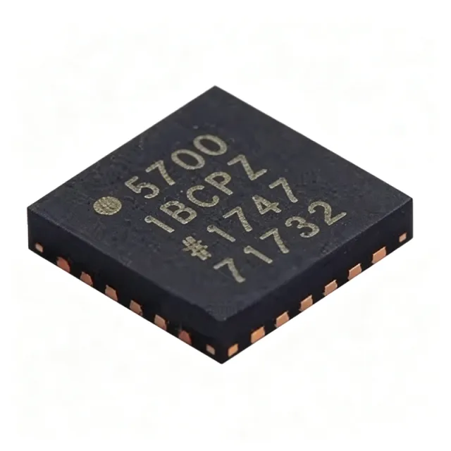
AD5700-1BCPZ - HART FSK Modem IC | Analog Devices

The AD5700-1BCPZ is a single-chip HART FSK half-duplex modem from Analog Devices, designed to comply with the HART physical layer requirements. It integrates all necessary filtering, signal detection, modulation, demodulation, and signal generation functions, requiring few external components. The device operates from a 2.7V to 5.5V supply and features an internal oscillator, eliminating the need for an external crystal. It is available in a compact 24-lead LFCSP-WQ (4x4 mm) package, making it ideal for space-constrained industrial applications. A HART modem is a specialized integrated circuit that enables communication over legacy 4-20 mA analog loops by superimposing a digital frequency-shift keying (FSK) signal. The HART protocol uses two frequencies: 1200 Hz for logic '1' and 2200 Hz for logic '0', allowing simultaneous analog and digital communication. The AD5700-1BCPZ is part of the HART modem product family, which falls under the broader category of industrial communication ICs, specifically interface ICs for process automation. Key features of the AD5700-1BCPZ include a low power consumption of 1 mA typical, an integrated receive band-pass filter that can be bypassed, and an internally buffered HART output with high drive capability. The device also includes an internal 2.5V reference and supports a wide operating temperature range of -40°C to +125°C. The LFCSP package provides excellent thermal performance and a small footprint, suitable for high-density designs. Technically, the AD5700-1BCPZ uses a digital signal processing (DSP) architecture to implement the HART modem functions, ensuring accurate and reliable communication. The integrated filter eliminates the need for external components, simplifying the design and reducing bill of materials cost. The device is fully compliant with the HART physical layer specification, ensuring interoperability with other HART-compliant devices. Typical applications include industrial process control, smart transmitters, valve positioners, and other field instruments that require HART communication. The low power consumption and small package make it suitable for loop-powered devices where power budget is critical. The internal oscillator further reduces component count, making it an excellent choice for compact designs. When designing with the AD5700-1BCPZ, ensure proper decoupling of the power supply and careful layout of the analog and digital sections to minimize noise. The device requires a few external components, including a coupling capacitor and a protection circuit for the HART signal path. Refer to the datasheet for detailed application circuits and recommended component values.

USD $6.68 Contact
AD5700-1BCPZ-RL - HART Modem IC with Oscillator | Analog Devices
AD5700-1BCPZ-RL

AD5700-1BCPZ-RL - HART Modem IC with Oscillator | Analog Devices

The AD5700-1BCPZ-RL is a single-chip HART FSK half-duplex modem from Analog Devices, designed to comply with the HART physical layer requirements. It integrates all necessary filtering, signal detection, modulation, demodulation, and signal generation functions, requiring few external components. The device operates from a 2.7V to 5.5V supply and features an integrated oscillator, eliminating the need for an external crystal. It is available in a compact 24-lead LFCSP-WQ (4x4 mm) package, suitable for space-constrained industrial applications. A HART modem is a specialized integrated circuit that enables communication over legacy 4-20 mA analog loops by superimposing a frequency-shift keying (FSK) digital signal. The AD5700-1 is part of the HART modem product family, which falls under the broader category of industrial communication ICs. These devices are essential in process automation, allowing digital configuration and diagnostics without disrupting analog measurement signals. Key features include a low-power design with a typical supply current of 86 µA in listen-only mode, an integrated receive band-pass filter that can be bypassed, and an internally buffered HART output for high drive capability. The device also includes an internal reference, a RESET pin for power-down mode, and a REF_EN pin to control the internal reference. The integrated oscillator provides a precise 1.2 MHz clock, simplifying the design and reducing component count. The AD5700-1 uses a digital signal processing (DSP) architecture to implement the HART protocol, ensuring reliable communication over long cable runs. The device supports data rates of 1200 bps, the standard HART speed, and is fully compliant with the HART physical layer specification. The LFCSP package offers excellent thermal performance and a small footprint, making it ideal for loop-powered transmitters and other compact field instruments. Typical applications include industrial process control, smart transmitters, valve positioners, and other field instruments that require HART communication. The device interfaces easily with Analog Devices' industrial converters, such as the AD5421 loop-powered current-output DAC, enabling complete smart transmitter solutions. When designing with the AD5700-1, ensure proper decoupling on the supply pins and follow the recommended layout in the datasheet to minimize noise. The RESET pin can be used to place the device in power-down mode, reducing current consumption to 1 µA, which is critical for loop-powered applications.

RFQ Contact
AD5700-1BCPZ-RL7 - Low Power HART Modem | Analog Devices
AD5700-1BCPZ-RL7

AD5700-1BCPZ-RL7 - Low Power HART Modem | Analog Devices

The AD5700-1BCPZ-RL7 is a single-chip HART FSK half-duplex modem from Analog Devices, designed to meet HART physical layer requirements for industrial field instrumentation. Housed in a 24-LFCSP-WQ (4x4) package, this low-power modem operates from a 1.71 V to 5.5 V supply and draws a maximum of 115 µA in receive mode, making it suitable for loop-powered and intrinsically safe applications. The AD5700-1 variant integrates a precision internal oscillator, eliminating the need for an external crystal and reducing component count and board area. A HART modem is a communication IC that superimposes digital Frequency Shift Keying (FSK) signals onto a 4-20 mA analog current loop, using 1200 Hz and 2200 Hz sinusoidal tones to represent logic '1' and logic '0'. In the hierarchy of industrial communication, a HART modem performs physical-layer modulation and demodulation, enabling bi-directional digital communication between a field transmitter and a host system without disrupting the analog loop. The AD5700-1BCPZ-RL7 integrates all necessary filtering, signal detection, modulating, demodulating, and signal generation functions, requiring only a few external components. Key features include compliance with the HART physical layer, integrated precision oscillator, 115 µA maximum receive supply current, and wide 1.71 V to 5.5 V operating range. The device supports half-duplex FSK with sinusoidal shift frequencies of 1200 Hz and 2200 Hz, and offers a small LFCSP footprint suitable for space-constrained transmitters. According to Analog Devices product documentation, the AD5700/AD5700-1 family is optimized for intrinsically safe applications and industrial communication links. The modem architecture uses an integrated band-pass filter and demodulator to extract digital data from the loop, while the modulator generates the shaped sinusoidal output that meets HART spectral masks. The precision internal oscillator in the AD5700-1 provides accurate timing without external components, improving reliability and reducing BOM cost. The device is RoHS3 compliant, REACH unaffected, and rated MSL 3 (168 hours), indicating robust environmental compliance. Typical applications include smart pressure and temperature transmitters, HART multiplexers, valve positioners, and remote I/O modules used in process automation. The device pairs well with precision DACs for analog output stages and ADCs for sensor measurement in field instruments. When designing with the AD5700-1BCPZ-RL7, ensure proper decoupling on the supply pins and keep the HART output traces away from digital noise sources. Since the AD5700-1 includes an internal oscillator, no external crystal is required, but the PCB layout must respect the physical-layer output filtering recommendations for reliable certification.

RFQ Contact
AD570JD/+ - 8-Bit Parallel SAR ADC | Analog Devices
AD570JD/+

AD570JD/+ - 8-Bit Parallel SAR ADC | Analog Devices

The Analog Devices AD570JD/+ is an 8-bit, single-channel successive-approximation analog-to-digital converter with parallel output, bipolar input capability, and an 18-pin SBDIP package. The converter incorporates a DAC, voltage reference, clock, comparator, successive-approximation register, and output buffers on one monolithic chip. The official product page lists the AD570 family price starting at $131.98 as of 2026-10-28, although a separate distributor listing quotes $83.28 for AD570JD/+. An ADC is an integrated circuit that converts a continuously varying analog voltage into a digital numerical representation. The AD570 belongs to the successive-approximation ADC category, a sampled-data architecture commonly used for instrumentation, industrial control, process monitoring, data acquisition, and embedded measurement systems. Within the signal-chain hierarchy, it sits between a sensor or conditioning circuit and a digital controller, processor, display, or communications interface. The AD570's 8-bit resolution provides 256 discrete output codes, while its single parallel output structure exposes the converted word directly on digital output pins. This architecture avoids adding a serial interface such as SPI or I2C. The monolithic implementation includes the reference, clock, comparator, DAC, successive-approximation register, and output buffers, reducing the number of external signal-conditioning and conversion components required for a basic parallel-output ADC design. According to the manufacturer datasheet, the converter uses integrated injection logic, or I2L, technology for the successive-approximation function. It also incorporates a laser-trimmed silicon-chromium thin-film resistor ladder network and a temperature-compensated subsurface Zener reference. These details indicate that the AD570 combines a complete conversion system with precision-oriented passive and reference elements rather than relying entirely on external components. Typical uses include industrial panel meters, temperature-controller input channels, laboratory measurement equipment, legacy data-acquisition systems, and embedded control boards that accept bipolar analog signals and produce an 8-bit parallel result. The 18-pin through-hole package is particularly useful for legacy instrument designs and prototypes assembled with conventional through-hole PCB footprints. Designers should verify the complete AD570 electrical specification from the manufacturer datasheet before replacing or updating a circuit, especially input range, reference behavior, acquisition timing, output logic levels, and temperature limits. Because the AD570 is marked not recommended for new designs, it is better suited to maintaining proven equipment than to starting a new platform without reviewing the current Analog Devices portfolio. This page consolidates the verified manufacturer description, distributor pricing references, package information, lifecycle status, alternative-device analysis, and practical design guidance. It also distinguishes documented facts from parameters that must be confirmed in the datasheet before creating a new PCB or replacing the converter in production equipment.

RFQ Contact
AD570SD - 8-Bit SAR ADC, 25 us, 18-Pin DIP | Analog Devices
AD570SD

AD570SD - 8-Bit SAR ADC, 25 us, 18-Pin DIP | Analog Devices

The Analog Devices AD570SD is a complete 8-bit successive-approximation analog-to-digital converter with one analog input, approximately 25 microseconds conversion time, and an 18-pin ceramic dual in-line package. It guarantees no missing codes over its specified -55°C to +125°C operating range and includes a voltage reference, clock, comparator, successive-approximation register, and output buffers on one monolithic chip. An ADC converts a continuous analog voltage into a digital number for measurement, control, display, and communications systems. The AD570 belongs to the successive-approximation ADC hierarchy, where a comparator successively tests internal DAC levels against the input. This SAR architecture offers deterministic sampling and conversion timing, making the AD570SD useful when a compact, self-contained converter is preferable to a higher-resolution or more complex ADC. The principal characteristics are 8-bit resolution, one analog input, approximately 25 microseconds conversion time, and no missing codes throughout the temperature range. The device uses digital multiplexing and three-state outputs, allowing multiple converters or external signals to share common output buses in suitable system arrangements. Its monolithic construction combines the converter, reference, clock, and output circuitry in one package. Operation is guaranteed with -15 V and +5 V supplies, and the device also operates with a -12 V supply. This combination supports bipolar input conversion with separate negative and positive supply rails. The AD570S family is available in a temperature version covering -55°C to +125°C, while the AD570SD/883B version is processed to MIL-STD-883C Class B according to the manufacturer product page. Typical uses include industrial process measurement, temperature and pressure instrumentation, laboratory data acquisition, legacy industrial controls, and embedded systems requiring an eight-bit measurement channel. Its extended-temperature specification makes it appropriate for harsh environments when the system must preserve full eight-bit accuracy and avoid missing output codes. Designers should preserve the required supply sequencing and logic-level constraints stated in the manufacturer datasheet. Because the output interface uses multiplexing and three-state outputs, the system must place each output into a valid state only when its associated data is being read. Decoupling, input grounding, and acquisition timing should be evaluated against the approximately 25-microsecond conversion requirement. This page combines converter architecture, temperature-range guidance, application fit, pin-package considerations, and drop-in replacement analysis. It also distinguishes standard, military, and extended-temperature AD570 family options so engineers can select the appropriate package and qualification level for the target system.

RFQ Contact
AD570SD/883B - 8-Bit ADC, 25us, MIL-STD-883B | Analog Devices
AD570SD/883B

AD570SD/883B - 8-Bit ADC, 25us, MIL-STD-883B | Analog Devices

The AD570SD/883B is a monolithic 8-bit successive approximation analog-to-digital converter (ADC) manufactured by Analog Devices, processed to MIL-STD-883B Class B for military and high-reliability applications. It integrates a DAC, voltage reference, clock, comparator, successive approximation register, and output buffers on a single chip, requiring no external components for a full-accuracy 8-bit conversion in 25 microseconds. The device operates from -15 V and +5 V supplies (also functional with -12 V) and is packaged in a side-brazed ceramic DIP-18 (SBDIP) with an operating temperature range of -55°C to +125°C. An analog-to-digital converter (ADC) is an electronic component that converts continuous analog signals into discrete digital numbers, enabling digital systems to process real-world signals. The AD570 is a successive approximation ADC, a type that uses a binary search algorithm to converge on the digital representation, balancing speed and resolution. It belongs to the broader category of data converters, which are essential in signal processing chains bridging analog sensors and digital processors. Key features include 8-bit resolution, a conversion time of 25 microseconds, and a parallel output interface with 8-bit access. The device offers unipolar and bipolar input ranges, with full-scale calibration and offset adjustments. It is guaranteed to operate with -15 V and +5 V supplies, and also supports -12 V operation. The military-grade processing ensures reliability in harsh environments, with a temperature range of -55°C to +125°C. Technically, the AD570 integrates all conversion functions on a single chip, eliminating the need for external clock or reference components. The successive approximation architecture provides a deterministic conversion time, making it suitable for real-time sampling. The device features a tri-state output buffer for bus-oriented systems, and its bipolar input capability allows direct connection to bipolar analog signals without external level shifting. Typical applications include military avionics, industrial process control, data acquisition systems, and test and measurement equipment where high reliability and wide temperature operation are critical. The AD570SD/883B is particularly suited for legacy military systems requiring a drop-in replacement for the original AD570. When designing with this device, ensure proper supply decoupling and consider the input impedance and settling time for accurate conversions. The device's parallel interface simplifies connection to microprocessors, but timing requirements must be observed for reliable data transfer.

RFQ Contact
AD571JD - 10-Bit SAR ADC with Reference | Analog Devices
AD571JD

AD571JD - 10-Bit SAR ADC with Reference | Analog Devices

The Analog Devices AD571JD is a 10-bit, single-input successive-approximation analog-to-digital converter with an internal voltage reference and clock, packaged in an 18-pin ceramic DIP. It performs conversions in 40 microseconds maximum and provides three-state parallel digital outputs for connection to microprocessors, controllers, and data-acquisition systems. The converter integrates a DAC, voltage reference, clock, comparator, successive-approximation register, and output buffers on one monolithic chip. An ADC converts a time-varying analog voltage into a digital number representing its amplitude. The AD571 belongs to the SAR ADC hierarchy, where an internal DAC produces successive approximation voltages that are compared with the input. Its complete-converter architecture places the reference, clock, and output circuitry together, reducing the number of external components required for basic acquisition systems. The AD571JD provides 10-bit resolution, one analog input channel, and a maximum conversion time of 40 microseconds. Three-state outputs permit multiple converters to share a common data bus when only one device is selected at a time. The monolithic construction supports a compact implementation, while the 18-pin ceramic DIP package facilitates replacement and prototyping in through-hole systems. The AD571 combines a 10-bit DAC, voltage reference, oscillator or clock section, comparator, successive-approximation register, and buffered outputs. According to the manufacturer documentation, the converter is designed for no missing codes over temperature up to +125 degrees Celsius. The parallel interface exposes the conversion result directly rather than using a serial protocol, making the device suitable for processor-controlled instrumentation where interface simplicity is important. Typical uses include industrial process measurement, laboratory data acquisition, digital panel meters, and embedded control systems that sample slowly varying analog signals. Its integrated reference and clock also suit educational or prototype systems where a complete standalone converter is more useful than a bare ADC core. The parallel output can connect to suitable data buses when the host processor provides the required control signals and output enable timing. Designers should verify the analog input range, reference accuracy, acquisition timing, and output logic levels against the complete manufacturer datasheet before layout. Because this is a ceramic DIP rather than a surface-mount device, board footprint and mechanical clearance must match the specified 18-pin package exactly. Replacement should also account for temperature grade and screening options rather than relying only on the 10-bit resolution and 40-microsecond conversion-speed labels. This page consolidates verified manufacturer and distributor information, package-level replacement guidance, and practical selection considerations that help distinguish a true drop-in ceramic-DIP replacement from merely similar ADC products.

RFQ Contact
AD571KD/+ - 10-Bit SAR ADC in 18-Pin DIP | Analog Devices
AD571KD/+

AD571KD/+ - 10-Bit SAR ADC in 18-Pin DIP | Analog Devices

Analog Devices AD571KD/+ is a 10-bit successive-approximation analog-to-digital converter housed in an 18-pin ceramic dual in-line package. The converter integrates a digital-to-analog converter, voltage reference, clock, comparator, successive-approximation register, and output buffers on one monolithic chip. Its primary characteristics are 10-bit resolution, commercial temperature grade, through-hole construction, and an 18-terminal rectangular DIP package. An ADC is an interface component that converts an analog voltage into a digital number for processing, measurement, display, or control. The AD571 belongs to the successive-approximation, or SAR, ADC family. In this architecture, an internal DAC generates successive trial voltages, the comparator evaluates each trial against the input, and the successive-approximation register records the conversion result. The AD571 integrates the supporting conversion elements on one chip, reducing the number of external components required for a complete conversion channel. The AD571's 10-bit conversion resolution provides 1,024 distinguishable digital codes across the converter's analog input range. This resolution is suitable for instrumentation and control systems that need moderate rather than high-resolution digital measurement. Its integrated reference, clock, comparator, DAC, register, and output buffers establish a self-contained conversion architecture, while the parallel output interface provides direct access to the converted code. The AD571KD/+ is identified as a commercial-grade, through-hole device in an 18-pin SBCDIP package. The ceramic DIP construction and through-hole lead format suit legacy industrial, instrumentation, test, and control equipment where plated-through-hole assembly and direct socket or PCB mounting are preferred. The package also provides a straightforward mechanical format for repair and replacement of older embedded analog-measurement systems. Typical applications include process-control instrumentation, digital panel meters, laboratory measurement equipment, sensor-interface circuits, industrial data-acquisition systems, and embedded control systems. In these systems, the AD571 can digitize a conditioned analog sensor signal while its integrated reference and conversion clock reduce the external support circuitry needed. System designers should still provide input conditioning, suitable bypassing, acquisition timing, and output-interface buffering. For a new design, verify the required analog input range, conversion timing, output logic levels, reference behavior, and acquisition architecture against the manufacturer datasheet before allocating the PCB footprint. When upgrading an existing board, confirm that the 18-pin pinout and signal functions match, and account for the DIP package's larger footprint compared with modern surface-mount ADC packages. This product page combines the AD571KD/+ device identity, package and converter architecture with replacement guidance, application-focused design guidance, and a parameter-by-parameter comparison. It is intended to help engineers identify the correct legacy-compatible ADC without confusing package variants, temperature grades, or functional alternatives with exact drop-in replacements.

RFQ Contact
AD571SD - 10-Bit SAR ADC with Reference | Analog Devices
AD571SD

AD571SD - 10-Bit SAR ADC with Reference | Analog Devices

The Analog Devices AD571SD is a 10-bit, single-input successive-approximation analog-to-digital converter integrated with a digital-to-analog converter, voltage reference, clock, comparator, successive-approximation register, and output buffers in an 18-pin SBDIP package. The device operates from a +5 V supply with a -12 V or -15 V analog supply, and it supports standard 0 V to +10 V unipolar or -5 V to +5 V bipolar input ranges. It is not recommended for new designs. A successive-approximation ADC is a data-converter category that compares an unknown analog voltage with successive internally generated reference levels. Each clock cycle resolves one additional bit, allowing a complete conversion to be completed in 10 clock periods. The AD571 integrates this conversion function with its supporting DAC and reference circuitry, reducing the number of external precision components required in conventional instrumentation designs. Key features include 10-bit resolution, one analog input channel, successive-approximation conversion, a complete on-chip reference and clock, parallel digital outputs, and integration of the principal converter blocks on one monolithic chip. The AD571 can be configured for 0 V to +10 V unipolar operation by connecting the bipolar-offset control to digital common, or for -5 V to +5 V bipolar operation by leaving that control open. The converter architecture compares the selected input against a DAC-generated trial voltage and uses a comparator to determine each successive-approximation decision. A 10-bit successive-approximation register retains the conversion result until the next conversion or a clear operation. Its integrated reference establishes the conversion scale, while the clock controls conversion timing and the output buffers provide compatible parallel digital outputs for external counters, processors, or display systems. Typical applications include digital voltmeters, process-control instrumentation, laboratory measurement equipment, industrial data-acquisition systems, and embedded measurement systems that require a parallel-output ADC. In these systems, the AD571 can reduce the need for a discrete reference and DAC, although its legacy interface and lifecycle status make it primarily appropriate for maintenance of existing equipment. Designers should account for the separate +5 V and negative analog supplies, connect analog and digital grounds according to the manufacturer's grounding guidance, and use suitable bypass capacitors at the supply pins. Sampling and clock timing should also be checked against the acquisition system so that acquisition time and conversion time provide sufficient settling before the result is read. This product page combines manufacturer specifications, lifecycle information, package details, application guidance, and verified cross-reference results for engineers maintaining an AD571SD-based design. It also distinguishes confirmed drop-in candidates from alternatives that would require different packages or electrical behavior.

RFQ Contact
AD571SD/883B - 10-Bit A/D Converter | Analog Devices | Military
AD571SD/883B

AD571SD/883B - 10-Bit A/D Converter | Analog Devices | Military

The AD571SD/883B is a complete 10-bit successive approximation analog-to-digital converter (ADC) from Analog Devices, designed for high-reliability military and aerospace applications. It integrates a precision voltage reference, clock, and comparator in a single 18-pin side-brazed ceramic DIP (SBDIP) package, offering a compact and robust solution for converting analog signals to digital data. The device accepts either unipolar (0 V to +10 V) or bipolar (-5 V to +5 V) analog inputs, selectable by grounding or opening a single pin, and provides true 10-bit accuracy with no missing codes over its full operating temperature range of -55°C to +125°C. An analog-to-digital converter (ADC) is an electronic component that transforms a continuous analog voltage into a discrete digital number proportional to the amplitude of the signal. The AD571SD/883B is a successive approximation register (SAR) ADC, which uses a binary search algorithm to determine the digital output. SAR ADCs are known for their high speed and moderate resolution, making them suitable for a wide range of data acquisition systems. In the hierarchy of signal processing, the ADC sits between the analog sensor/amplifier and the digital processor, serving as the critical bridge that enables digital systems to interpret real-world analog signals. Key features of the AD571SD/883B include a 10-bit resolution, a maximum conversion time of 25 microseconds, and a parallel digital interface for easy connection to microprocessors and digital logic. The device operates from dual supplies of +5 V and -12 V or -15 V, and includes an internal clock and reference, eliminating the need for external components. The military-grade screening (883B) ensures compliance with MIL-STD-883, providing enhanced reliability for demanding environments. Technically, the AD571SD/883B employs a laser-trimmed thin-film resistor network and a high-speed comparator to achieve its accuracy. The device features a full-scale calibration capability, allowing users to adjust the gain and offset for precise measurements. The bipolar offset and unipolar offset pins provide flexibility in configuring the input range, while the differential nonlinearity is guaranteed to be within ±1 LSB over the entire temperature range. Typical applications include military avionics, radar systems, industrial process control, and high-reliability data acquisition systems. The device's wide operating temperature range and hermetic ceramic package make it ideal for harsh environments where standard commercial ADCs would fail. When designing with the AD571SD/883B, ensure that the analog input is properly buffered and that the power supplies are well-decoupled to minimize noise. The internal reference is trimmed at the factory, but external calibration may be required for absolute accuracy in critical applications.

RFQ Contact
AD572AD - 12-Bit Successive Approximation ADC | Analog Devices
AD572AD

AD572AD - 12-Bit Successive Approximation ADC | Analog Devices

The Analog Devices AD572AD is a complete 12-bit successive-approximation analog-to-digital converter with an internal clock, reference, comparator, and buffer amplifier, housed in a 32-pin through-hole DIP package. The converter supports parallel and serial data transfer, according to product listings, and uses a hybrid integrated-circuit construction that combines MSI digital circuitry with linear monolithic chips. Its high-stability thin-film resistors are actively laser trimmed to improve accuracy, repeatability, and production consistency. An ADC is a data-conversion IC that transforms a continuously varying analog voltage into a digital code for processing, measurement, or control. The AD572 belongs to the ADC hierarchy, where it is more specifically a successive-approximation converter, sometimes called a SAR ADC. Unlike a flash converter, this architecture compares the input against successively refined internal references and therefore supports relatively high resolution with a practical internal circuit arrangement. The AD572AD's principal specifications include 12-bit resolution, differential input capability, parallel and serial output options, and a 32-pin DIP package. Its internal reference and buffer amplifier reduce the number of external signal-conditioning elements required for many measurement systems. Active laser trimming of thin-film resistors helps establish stable conversion characteristics without relying on ordinary uncorrected resistor tolerances. The hybrid construction is significant because it divides the converter into digital and linear functional blocks. The MSI digital section manages conversion sequencing and data output, while the monolithic linear section supports the reference, comparator, and signal-buffer functions. This architecture allows the converter to operate as a largely complete acquisition element rather than requiring a separate clock, reference source, comparator, and input buffer. AD572AD is suited to industrial process measurement, instrumentation, laboratory data acquisition, closed-loop control, and test systems where a 12-bit conversion result and selectable parallel or serial data handling are useful. The through-hole DIP format also suits legacy industrial equipment and prototypes assembled with conventional through-hole insertion methods. Designers should follow the Analog Devices AD572 datasheet for the exact analog input range, conversion timing, logic levels, reference behavior, and recommended decoupling. Because this converter combines an internal reference with analog input conditioning, stable grounding and careful routing of the analog and digital return paths remain important. Review the complete pin description table before assigning board nets or selecting bypass-capacitor locations. This product page consolidates the known resolution, converter architecture, package, interface options, and construction details with practical sourcing, application, comparison, and design guidance. It also distinguishes verified drop-in alternatives from merely similar converters, helping engineers make package and pin-compatibility decisions before committing to a replacement.

RFQ Contact
AD572BD - 12-Bit SAR ADC | Analog Devices | SBCDIP-32
AD572BD

AD572BD - 12-Bit SAR ADC | Analog Devices | SBCDIP-32

The Analog Devices AD572BD is a complete 12-bit successive-approximation analog-to-digital converter with parallel and serial interfaces, an internal clock, internal reference, comparator, and buffer amplifier, housed in a 32-pin SBCDIP package. The converter combines digital and linear monolithic elements with active laser trimming of high-stability thin-film resistors, providing a compact, complete solution for converting analog signals into 12-bit digital data. An ADC is an interface component that translates a continuously varying voltage into a numeric representation for processing by a microprocessor, controller, FPGA, or other digital system. The AD572 belongs to the data-converter hierarchy and uses the successive-approximation, or SAR, method. In this architecture, an internal successive-approximation register compares the input against a generated reference voltage, progressively refining the result until the converted code corresponds to the analog input. The AD572 integrates functions that would otherwise require separate clock, reference, comparator, and input-buffer circuitry. Its 12-bit resolution provides 4096 possible digital output codes. Parallel output supports direct connection to digital buses, while serial output reduces the number of signal interconnects when board space or connector availability is constrained. This combination gives engineers flexibility in how the converter is interfaced to the surrounding digital system. Active laser trimming of thin-film resistors improves the stability and matching of the internal resistor network. Trimming allows calibration during manufacture to reduce offsets and improve accuracy. The hybrid IC implementation combines MSI digital circuitry with linear monolithic chips, combining digital conversion control and analog measurement functions within one device. The internal reference and buffer amplifier also reduce the number of external precision components required for basic operation. The AD572 is suitable for industrial data acquisition, process-control instrumentation, test and measurement equipment, embedded control systems, and legacy computer interfaces. It is particularly appropriate when a design requires a complete 12-bit converter with both parallel and serial outputs rather than a high-speed streaming ADC. The tube packaging and 32-pin SBCDIP outline also suit instruments and industrial systems built around through-hole analog and mixed-signal assemblies. Designers should verify signal levels against the converter's input and reference ranges, establish the correct conversion timing for the selected interface, and provide suitable bypassing around the supply and analog input pins. Because this is a conventional through-hole hybrid converter, board area and interconnect length may favor a more modern surface-mount ADC, but the AD572BD can simplify qualification of older industrial platforms. This page combines the manufacturer's product information with engineering-oriented guidance on conversion interfaces, accuracy, application fit, and design considerations. It also distinguishes verified product characteristics from details that must be confirmed in the complete Analog Devices AD572 documentation before schematic release or production use.

RFQ Contact
AD573JD - 10-Bit SAR ADC | Analog Devices | Data Acquisition
AD573JD

AD573JD - 10-Bit SAR ADC | Analog Devices | Data Acquisition

Analog Devices AD573JD is a complete 10-bit successive-approximation analog-to-digital converter with an integrated reference, clock, and comparator, operating from +5 V and -12 V or -15 V supplies in a 20-pin hermetically sealed ceramic DIP package. It converts an analog input into a 10-bit digital result with a typical successive-approximation conversion time of 20 µs and supports full or 16-bit microprocessor-bus interfacing. An ADC is an interface IC that translates a continuously varying analog voltage into a digital code for processing, measurement, or control. The AD573 belongs to the SAR ADC family, whose internal comparator repeatedly selects residual-voltage bits until the 10-bit conversion is complete. Because the AD573 includes its reference, clock, and comparator, the manufacturer describes it as a complete converter requiring no external components to perform a conversion. The AD573's principal engineering features include a 10-bit conversion resolution, no missing codes over temperature, and operation from +5 V and either -12 V or -15 V supplies. These characteristics make it suitable for instrumentation, industrial monitoring, sensor measurement, data acquisition, and embedded control systems where a compact parallel-output ADC is appropriate. The AD573 family is available in multiple package configurations, including 20-pin hermetically sealed ceramic DIP. The manufacturer product page states that AD573J and AD573K versions can also be supplied in a 20-pin plastic DIP or 20-pin leaded chip carrier. The AD573JD ordering code identifies the hermetically sealed ceramic DIP configuration, whose package is suited to demanding temperature-range and reliability environments. Typical uses include digitizing transducer outputs in industrial measurement systems, acquiring slowly changing sensor signals in data-acquisition equipment, monitoring process variables in instrumentation, and feeding sampled analog data into microprocessor-based embedded controllers. The parallel digital interface simplifies connection to systems with dedicated data and control buses, while the integrated converter functions reduce external component count. Designers should verify the complete pinout, electrical limits, timing relationships, reference behavior, input range, and bus interface against the manufacturer datasheet before layout or replacement qualification. Because the device uses a negative supply alongside +5 V, bypassing and grounding must be planned carefully. A replacement should be accepted only when its package, pin assignment, logic levels, supply requirements, conversion timing, and temperature grade are verified as compatible. This page consolidates the verified AD573JD converter characteristics, package information, application guidance, sourcing caveats, and replacement constraints. It also distinguishes verified facts from parameters that still require confirmation from the manufacturer datasheet, helping engineers avoid treating an incomplete distributor listing as a complete design specification.

RFQ Contact
AD573JN - 10-Bit SAR ADC with 20 us Conversion | Analog Devices
AD573JN

AD573JN - 10-Bit SAR ADC with 20 us Conversion | Analog Devices

Analog Devices AD573JN is a complete 10-bit successive-approximation analog-to-digital converter with a 20 us typical conversion time, packaged in a 20-pin PDIP. It integrates a DAC, voltage reference, clock, comparator, successive-approximation register, and three-state output buffers on one monolithic chip, reducing the external circuitry required for a standalone data-acquisition front end. According to the Analog Devices AD573 product page, performance is guaranteed with +5 V and either -12 V or -15 V supplies, and a version compliant with MIL-STD-883 is available. An ADC converts a time-varying analog voltage into a numerical representation for processing by a microprocessor, controller, or other digital logic. The AD573 belongs to the SAR ADC hierarchy: during each conversion, its internal DAC generates successive trial voltages for the comparator, and the successive-approximation register records the binary result. This complete converter category includes the reference, clock, comparator, SAR logic, and digital output interface in one device. Key features include 10-bit resolution, one analog input, a typical successive-approximation conversion time of 20 us, no missing codes over temperature, operation from a +5 V supply with a negative -12 V or -15 V supply, and a monolithic implementation. Separate HBE and LBE inputs enable the eight most-significant bits or the two least-significant bits for straightforward connection to narrower microprocessor buses. The AD573JN uses a parallel digital interface rather than a serial protocol. The manufacturer datasheet identifies DB9 through DB2 on pins 10 through 3, with HBE on pin 20 and LBE on pin 19; DB1 and DB0 occupy pins 2 and 1. Its integrated reference, clock, comparator, and output buffering simplify system implementation, although the negative supply requirement and parallel-bus wiring remain important constraints. Typical uses include industrial process-control instrumentation, laboratory measurement equipment, legacy microprocessor data-acquisition systems, embedded control panels, and educational analog-measurement platforms. The 20 us typical conversion time favors sampled or multiplexed measurement systems rather than high-frame-rate waveform acquisition, while the 10-bit result provides approximately 1024 addressable output codes. Designers should verify input-range, reference, timing, and logic-level details against the manufacturer datasheet before layout. Decoupling, grounding, bus timing, and unused digital outputs require careful treatment because this legacy-style converter combines analog and digital functions in one package. The cited supply configurations should be followed exactly rather than assuming conventional single-supply operation. This product record consolidates manufacturer functionality, distributor package information, interface details, and verified drop-in candidates. It also separates documented specifications from unavailable parameters, making the engineering trade-offs and replacement uncertainty explicit rather than presenting unverified values as production-ready design data.

RFQ Contact
AD573JP - 10-Bit SAR ADC with Parallel Output | Analog Devices
AD573JP

AD573JP - 10-Bit SAR ADC with Parallel Output | Analog Devices

The Analog Devices AD573JP is a complete 10-bit successive-approximation analog-to-digital converter with integrated reference, clock, comparator, successive-approximation register, DAC, and three-state output buffers, packaged in a 20-pin PLCC. It converts one single-ended analog input into a 10-bit parallel digital result. The verified product information identifies the AD573 as a 10-bit SAR ADC with a typical conversion time of 20 µs, no missing codes over temperature, and operation using +5 V and -12 V or -15 V supplies. The AD573JP is specified for 20-PLCC, 9 x 9 mm packaging and is offered by distributors as a single-input, single-channel ADC. An ADC is an analog-to-digital converter, a category of data-conversion ICs that translates a continuously varying voltage into a numeric value. The AD573's successive-approximation architecture is a complete mixed-signal subsystem rather than only a comparator or front end. Within the hierarchy of semiconductor components, the AD573JP is an ADC, then a data-converter IC, then an integrated circuit. Its internal reference and parallel bus make it useful when an embedded controller needs direct digital access without an external reference or serial conversion interface. Key features include complete 10-bit conversion, integrated voltage reference and clock circuitry, parallel microprocessor-bus-compatible output, and three-state output buffers. The converter uses a successive-approximation conversion process rather than a flash or pipeline architecture. Its parallel interface can connect directly to suitable digital bus logic or microprocessor input circuitry, reducing the need for a serial protocol. The specified power-supply arrangement supports +5 V and either -12 V or -15 V analog supplies, so the device is intended for systems able to provide the required positive and negative rails. The AD573 architecture is relevant where a moderate-resolution measurement must be acquired deterministically and presented in parallel. Because the converter includes a DAC, voltage reference, clock, comparator, SAR register, and output buffers on one chip, the system designer can focus on input conditioning, bus interfacing, timing, and reference-quality requirements. Its 10-bit resolution represents 1024 quantization levels, while the 20 µs typical conversion time provides a defined sampling interval for industrial control, instrumentation, and legacy microprocessor systems. Typical applications include industrial process measurement, laboratory instrumentation, digital panel meters, transducer signal acquisition, and embedded control systems with parallel buses. The input front end still requires careful attention to source impedance, acquisition time, input range, grounding, and noise. The positive and negative supply requirements must be checked against the system power architecture before layout begins, especially when replacing the converter with a different ADC family. A key design consideration is bus contention. The three-state outputs allow multiple devices or bus transceivers to share parallel data lines, but the system must ensure that only one output driver is enabled at a time. Input settling, conversion control, and the relationship between the internal clock and external bus timing should be verified against the manufacturer datasheet. This product page consolidates verified manufacturer and distributor information, package details, sourcing links, functional guidance, and explicitly separated uncertainties. It distinguishes documented AD573JP characteristics from parameters that require confirmation from the complete manufacturer datasheet before layout or production release.

RFQ Contact
AD573KD/+ - 10-Bit Single-Input SAR ADC | Analog Devices
AD573KD/+

AD573KD/+ - 10-Bit Single-Input SAR ADC | Analog Devices

Analog Devices AD573KD/+ is a 10-bit, single-input successive-approximation analog-to-digital converter housed in a 20-pin ceramic DIP package. The converter uses a parallel digital interface, operates from +5 V and either -12 V or -15 V supplies, and requires no external components to perform a conversion. An ADC is a data-conversion IC that converts a time-varying analog voltage into a numeric representation. The AD573 belongs to the SAR ADC hierarchy, where successive-approximation conversion compares the input against internally generated reference levels. It is used when a system needs compact, standalone conversion rather than the throughput and integration provided by a more complex high-speed converter. The principal verified specifications are 10-bit resolution, one analog input, SAR architecture, and a 20-CDIP package. Performance is guaranteed with +5 V and -12 V or -15 V supplies. The AD573KD/+ also appears as a 20-CDIP component with 2.54 mm leads, while the broader AD573 family is offered in multiple package configurations. Its digital outputs are suitable for parallel-processing systems, instrumentation, and industrial control equipment. The AD573 family is a complete converter according to the manufacturer product page, and no external components are required to perform a conversion. This simplifies analog front-end design when the available input range and acquisition rate meet the application requirements. The single-ended input arrangement also keeps the signal interface straightforward, although system-level grounding and signal conditioning remain essential for reliable measurements. Typical uses include process monitoring, industrial data acquisition, instrumentation, laboratory equipment, and embedded control systems. Designs must accommodate the converter's separate positive and negative supply requirements and interface its parallel outputs correctly to the host controller, counter, latch, or digital bus. When laying out the AD573KD/+, place the device close to the analog source and provide suitable bypass decoupling on the supply pins. The ceramic DIP package is suited to conventional through-hole assembly rather than high-density surface-mount designs. Confirm the complete pinout and timing behavior against the manufacturer datasheet before finalizing routing. This page consolidates verified manufacturer and distributor information for the AD573KD/+, adds application-focused design context, distinguishes confirmed specifications from unavailable details, and clearly records that no verified pin-to-pin substitute was found rather than presenting a merely similar converter as a drop-in replacement.

RFQ Contact