Products (38,000+)

AD7475BRMZ-REEL - 12-Bit 1MSPS SAR ADC | Analog Devices
AD7475BRMZ-REEL

AD7475BRMZ-REEL - 12-Bit 1MSPS SAR ADC | Analog Devices

The Analog Devices AD7475BRMZ-REEL is a 12-bit, high-speed, low-power successive-approximation analog-to-digital converter (SAR ADC) that operates from a single 2.7 V to 5.25 V supply and delivers throughput rates up to 1 MSPS. Packaged in an 8-pin MSOP (RM-8) and supplied on a 7-inch reel, it integrates a low-noise, wide-bandwidth track-and-hold amplifier capable of handling input frequencies in excess of 1 MHz. The external 2.5 V reference applied at REF IN, combined with the on-chip serial interface, makes it well suited for compact mixed-signal designs. A SAR (Successive Approximation Register) ADC is a precision converter architecture that uses a binary-search algorithm against an internal DAC to digitize the input voltage in N clock cycles. SAR ADCs sit in the broader taxonomy of analog-to-digital converters -> data converters -> mixed-signal ICs -> signal chain semiconductors, and they are favoured over pipeline or flash ADCs where low latency, deterministic sampling, and low power consumption are required at moderate resolutions (8 to 16 bits). Key features include a 1 MSPS conversion rate, 4.5 mW typical power dissipation at full speed, a flexible serial (SPI/QSPI/MICROWIRE/DSP-compatible) interface, and the proprietary VDRIVE function that allows the digital I/O logic levels to be set independently of the analog supply. The device offers a typical INL of ±1 LSB and operates across the industrial -40C to +85C temperature range, ensuring stable performance in harsh environments. From an architectural standpoint, the AD7475 uses a charge-redistribution DAC array combined with a high-bandwidth sample-and-hold capable of digitizing signals well beyond the Nyquist frequency. The serial clock can be applied up to 20 MHz, supporting the full 1 MSPS throughput while keeping the digital interface noise isolated from the analog input stage, an essential consideration for high-precision measurement systems. Typical applications include battery-powered instrumentation, portable data acquisition systems, optical sensor front-ends, isolated industrial process controls, and precision medical instruments such as patient monitoring devices. Designers also deploy it in motor control feedback loops and programmable logic controller (PLC) analog input modules where deterministic latency and low power are equally important. When designing with this device, ensure the reference decoupling capacitor is placed as close as possible to the REF IN pin and use a clean, low-noise analog ground pour to preserve 12-bit accuracy. The VDRIVE pin should be tied to the host MCU's logic supply to guarantee proper SPI timing margins at full 1 MSPS throughput. This page synthesizes distributor pricing, drop-in compatible replacements, and practical PCB layout notes that extend beyond the manufacturer datasheet, giving engineers a single authoritative reference for the AD7475BRMZ-REEL.

RFQ Contact
AD7476AAKSZ-REEL - 12-bit 1MSPS SAR ADC SC-70 | ADI
AD7476AAKSZ-REEL

AD7476AAKSZ-REEL - 12-bit 1MSPS SAR ADC SC-70 | ADI

The Analog Devices AD7476AAKSZ-REEL is a 12-bit, 1 MSPS successive-approximation register (SAR) analog-to-digital converter (ADC) housed in a 6-lead SC-70 package. It operates from a single 2.35 V to 5.25 V power supply, consumes low power, and provides one analog input channel with a throughput rate up to 1 MSPS. An ADC is a data converter that transforms a continuous analog voltage into a discrete digital code. SAR (Successive Approximation Register) ADCs use a binary-search algorithm combined with an internal DAC to resolve each conversion in a fixed number of clock cycles, balancing speed, accuracy, and power efficiency. Within the converter hierarchy, this places the AD7476A in the precision, low-power, successive-approximation sub-family, well-suited for battery-powered and space-constrained instrumentation. Key features of the AD7476A include 12-bit resolution, 1 MSPS throughput, a wide 2.35 V to 5.25 V single-supply input range, low power consumption, and a small 6-lead SC-70 outline. The -REEL suffix denotes tape-and-reel packaging for high-speed pick-and-place assembly. The part shares pinout with the 10-bit AD7477A and 8-bit AD7478A, allowing designers to migrate resolution by simply changing the device. Typical applications include portable and battery-powered systems, instrumentation, data acquisition front-ends, optical sensor front-ends, and general-purpose analog monitoring in industrial, medical, and consumer designs. The SC-70 footprint makes it attractive where PCB real estate is at a premium. When designing with this device, provide adequate decoupling near the supply pin and ensure the analog input is bandwidth-limited to avoid aliasing. The wide supply range simplifies integration into both 3.3 V and 5 V systems. This page synthesizes distributor pricing, verified pin-compatible alternatives, and practical design notes curated for engineers — beyond what is found in the manufacturer datasheet.

RFQ Contact
AD7476ABKSZ-REEL - 12-Bit 1 MSPS SAR ADC, SC-70-6 | Analog Devices
AD7476ABKSZ-REEL

AD7476ABKSZ-REEL - 12-Bit 1 MSPS SAR ADC, SC-70-6 | Analog Devices

The Analog Devices AD7476ABKSZ-REEL is a 12-bit, 1 MSPS successive-approximation register (SAR) analog-to-digital converter housed in a 6-lead SC-70-6 package. It operates from a single 2.35 V to 5.25 V power supply, features a single-ended analog input, and is rated over the -40C to +85C industrial temperature range. The part pairs a 12-bit resolution with throughput up to 1 million samples per second, making it one of the smallest form-factor high-speed ADCs in the ADI portfolio. An SAR ADC is a type of data converter that uses a successive-approximation register and an internal track-and-hold to digitize an analog input in a fixed number of clock cycles (typically one per N-bit cycle). As a sub-family of Nyquist-rate data converters, SAR ADCs sit between sigma-delta converters (higher resolution, lower speed) and flash ADCs (highest speed, lowest resolution) within the ADC taxonomy. ADCs are integrated circuits that bridge real-world analog signals to digital processors and microcontrollers across the broader mixed-signal and data-acquisition IC hierarchy. Key features include very low power consumption, a high-speed SPI/QSPI/MICROWIRE-compatible serial interface, and an automatic power-down between conversions that drops current draw dramatically when the part idles between samples. The 6-lead SC-70 footprint makes it one of the smallest 1 MSPS ADCs available, enabling analog front-end placement next to sensors on space-constrained PCBAs. The device uses a charge redistribution DAC architecture with an internal reference and a high-bandwidth input track-and-hold to deliver 12-bit linearity across the full input common-mode range. Because conversion is deterministic in time (no pipeline latency), the AD7476A is well suited to event-triggered sampling, multiplexed-channel sequencing, and motor-control feedback loops where deterministic group delay is required. Typical applications include battery-powered portable instrumentation, hand-held multimeters and data loggers, transducer signal conditioning chains, isolated industrial sensors, optical-module monitoring, and general-purpose embedded analog front ends. Designers select this part specifically when PCB area, single-rail operation, and deterministic conversion latency are more important than the very highest absolute sampling rates. When laying out a board, place the 0.1uF supply-decoupling capacitor as close as possible to the VDD pin, keep analog and digital grounds separated with a single-point stitch near the IC, and route the SCK, SDATA, and /CS digital traces away from the analog input net. Always drive /CS low before SCK edges and observe the tCONVERT timing budget for accurate 1 MSPS operation. This page synthesizes ADI distributor pricing, drop-in alternatives, and SC-70 layout/design notes that go beyond the bare datasheet to give you a faster procurement and bring-up decision.

RFQ Contact
AD7476ARTZ-REEL - 12-Bit 1MSPS SAR ADC SOT-23-6 | ADI
AD7476ARTZ-REEL

AD7476ARTZ-REEL - 12-Bit 1MSPS SAR ADC SOT-23-6 | ADI

The Analog Devices AD7476ARTZ-REEL is a 12-bit, 1 MSPS successive-approximation-register (SAR) analog-to-digital converter in a 6-lead SOT-23 package, delivering high-speed acquisition in the industry's smallest footprint for its performance class. It operates from a single 2.35 V to 5.25 V supply, draws only 3.6 mW typical at 1 MSPS with a 3 V supply, and integrates a low-noise wide-bandwidth track-and-hold amplifier capable of handling input frequencies beyond 6 MHz with 70 dB SNR at 100 kHz input. A SAR ADC is a successive-approximation-register analog-to-digital converter that uses a binary-search algorithm against an internal DAC to convert an analog input to a digital code in N clock cycles for N-bit resolution. In the broader signal-chain taxonomy, SAR ADCs sit between flash converters (fastest, lowest resolution) and sigma-delta ADCs (slowest, highest resolution), making them the optimal choice when an application needs single-cycle latency, moderate-to-high speed, and 8-16 bit resolution. The AD7476 belongs to the data-converter hierarchy: ADC -> SAR ADC -> 12-bit ADC -> low-power precision ADC, and is widely used as a system-side companion to microcontroller ADCs when higher speed or accuracy is required. Key features include flexible power/serial-clock-speed management that scales consumption with throughput, a high-speed serial interface compatible with SPI/QSPI/MICROWIRE/DSP, pseudo-differential analog input referenced to GND, and an operating temperature range of -40C to +85C. The 1 MSPS throughput makes the part suitable for multiplexed multi-channel systems where channels are scanned in sequence. Typical applications include portable and battery-powered instrumentation, industrial process control loops, optical module monitoring, motor-control current sensing, and data-acquisition front-ends. Designers benefit from the part's small SOT-23-6 footprint when board real estate is constrained, and from its 3.6 mW dissipation when thermal or battery budgets are tight. When designing with this ADC, budget for at least 3 acquisition-clock cycles before conversion starts to settle the track-and-hold fully, and place the 0.1 uF decoupling capacitor as close as possible to the VDD pin to preserve SNR. Average supply current scales linearly with throughput, so the part is equally well-suited to high-speed burst sampling and continuous low-rate conversion. This page synthesizes distributor stock, parametric drop-in alternatives, and practical SOT-23 layout guidance beyond the manufacturer datasheet.

RFQ Contact
AD7476BRTZ-REEL - 12-bit 1MSPS SAR ADC | Analog Devices
AD7476BRTZ-REEL

AD7476BRTZ-REEL - 12-bit 1MSPS SAR ADC | Analog Devices

The Analog Devices AD7476BRTZ-REEL is a 12-bit, 1 MSPS, successive-approximation analog-to-digital converter (SAR ADC) housed in a 6-pin SOT-23 (RT) package. It operates from a single 2.35 V to 5.25 V supply, draws a low supply current, and features a wide-bandwidth track-and-hold front end capable of handling input frequencies above 6 MHz. A successive-approximation ADC is a type of data converter that resolves the input voltage one bit per clock cycle against an internal precision DAC, producing a deterministic, low-latency conversion with no pipeline delay. SAR ADCs sit within the broader hierarchy of analog-to-digital converter -> data converter -> mixed-signal IC -> semiconductor, and are favored where low latency, small package size, and ease of use matter more than the very highest conversion rates. The AD7476 family (AD7476/AD7477/AD7478) shares this architecture at 12-, 10-, and 8-bit resolutions respectively. Key specifications include 1 MSPS throughput, 12-bit resolution with no missing codes, a wide input bandwidth exceeding 6 MHz, and an on-chip low-noise track-and-hold amplifier. The part integrates a high-speed serial interface (SPI/QSPI/MICROWIRE-compatible), consumes low power at full speed, and offers flexible input ranges supporting both unipolar and bipolar operation when driven through an appropriate driver or reference. Architecturally, the AD7476 uses a charge-redistribution capacitive DAC core with internal auto-calibration, which provides excellent DC accuracy and low integral nonlinearity across temperature. Its serial interface saves board area and simplifies isolation compared to parallel-output converters of similar speed. Typical applications include portable instrumentation, data acquisition systems, battery-powered equipment, isolated industrial front ends, and precision sensor signal chains. The tiny SOT-23-6 footprint and 1 MSPS rate make it well-suited for compact, low-power designs that still require good DC accuracy. When designing with this part, place the supply decoupling capacitor (typically 100 nF) within 5 mm of the AVDD pin and keep digital traces away from the analog input. For best linearity, drive the input with a low-impedance op-amp buffer rather than a high-impedance source. This page synthesizes distributor pricing, drop-in SOT-23-6 alternatives, and practical design notes not consolidated on the manufacturer datasheet alone.

RFQ Contact
AD7477ARTZ-REEL - 10-Bit 1MSPS SAR ADC SOT-23-6 | Analog Devices
AD7477ARTZ-REEL

AD7477ARTZ-REEL - 10-Bit 1MSPS SAR ADC SOT-23-6 | Analog Devices

The Analog Devices AD7477ARTZ-REEL is a 10-bit, 1 MSPS successive-approximation-register (SAR) analog-to-digital converter in a 6-lead SOT-23 package. The part operates from a single 2.35 V to 5.25 V power supply and features one analog input channel with a serial SPI/QSPI/MICROWIRE/DSP-compatible data interface. Its throughput rate of up to 1 MSPS makes it one of the fastest ADCs available in a SOT-23-6 footprint. A SAR ADC is a successive-approximation-register converter that uses a binary-search algorithm and an internal capacitive DAC to convert an analog input into a digital codeword. Within the data-converter hierarchy, SAR ADCs sit between flash converters (faster, lower resolution, higher power) and sigma-delta ADCs (slower, higher resolution, excellent noise). They occupy the niche where moderate-to-high speed, low latency, and low power consumption are required without the latency penalty of oversampling converters. Key features of the AD7477ARTZ-REEL include 70 dB SNR at 100 kHz input, wide input bandwidth, low power at 1 MSPS with both 3 V and 5 V supplies, and a small SOT-23-6 footprint that enables dense PCB layouts. The wide supply range lets a single device operate across 3.3 V and 5 V system rails, simplifying multi-rail designs and reducing inventory variants. The internal architecture combines an input sampling network, a precision comparator, a successive-approximation register with a 10-bit DAC, and a serial output engine. The 70 dB SNR translates to roughly 11.3 effective bits at full speed, sufficient for industrial monitoring, motor-control feedback loops, and instrumentation front-ends where 10-bit absolute accuracy is required. Typical applications include battery-management systems, portable instrumentation, data acquisition front-ends, optical-module monitoring, and general-purpose embedded analog signal conditioning. The small package makes it well suited to space-constrained designs such as handheld test equipment and IoT sensor nodes. When designing with the AD7477ARTZ-REEL, observe proper analog-input driving and decoupling: use a low-impedance buffer or RC network at AIN, and place 100 nF bypass capacitors as close to VDD and GND as possible to preserve SNR at full 1 MSPS throughput. This page consolidates manufacturer specifications, distributor pricing as of 2026-10-12, drop-in alternatives, and practical design notes drawn from the Analog Devices datasheet family to support fast, accurate component selection.

RFQ Contact
AD7477SRTZ-REEL - 10-Bit 1MSPS SAR ADC | Analog Devices
AD7477SRTZ-REEL

AD7477SRTZ-REEL - 10-Bit 1MSPS SAR ADC | Analog Devices

The Analog Devices AD7477SRTZ-REEL is a 10-bit, high-speed, low-power successive approximation register (SAR) analog-to-digital converter with a 1 MSPS sampling rate in a 6-pin SOT-23 (RT) package. It operates from a single 2.35 V to 5.25 V supply, drawing only 4 mA typical at 1 MSPS with VDD = 3 V, and provides a versatile SPI/QSPI/MICROWIRE/DSP-compatible serial interface. A SAR ADC is a type of data converter that uses a binary-search successive-approximation algorithm to digitize an analog input one bit at a time within a single clock cycle per bit. SAR ADCs occupy the middle ground between flash ADCs (fastest, lowest resolution) and sigma-delta ADCs (highest resolution, lower speed). They are widely used in industrial, instrumentation, and motor-control applications where deterministic latency, low latency-to-sample delay, and moderate-to-high sampling rates are required without the cost of higher-end delta-sigma parts. The AD7477 family sits in the precision Analog Devices portfolio alongside its 8-bit (AD7478) and 12-bit (AD7476) siblings. Key features of the AD7477SRTZ-REEL include throughput up to 1 MSPS, an analog input range of 0 V to VDD, true bipolar input capability with a resistor network, an on-chip track-and-hold amplifier, and a high-speed serial interface. The device includes an on-chip reference input (REF) and a low-noise, wide-bandwidth track-and-hold capable of handling input frequencies well above the Nyquist limit. Power-down current is typically 1 µA, making the part suitable for battery-powered and portable designs. Architecturally, the AD7477 uses a charge-redistribution DAC array controlled by a SAR logic core. The analog input is sampled on an internal capacitor array, then compared against binary-weighted capacitors in successive approximation cycles, yielding 10 bits in 10 conversion cycles. The serial output appears MSB-first on SDOUT, clocked by SCLK. The compact SOT-23-6 footprint measures only 2.9 mm × 1.6 mm and offers an exposed pad for thermal dissipation and reduced ground inductance. Typical applications include industrial process control, portable data acquisition, battery-powered instruments, motor control feedback, and transducer interfacing. The wide 2.35 V – 5.25 V supply range allows direct interfacing to 3.3 V and 5 V microcontrollers, while the SPI-compatible serial interface ensures easy connection to DSPs and microcontrollers without glue logic. When designing with the AD7477, ensure the reference voltage source has low impedance at the REF pin - a 10 µF decoupling capacitor close to the pin is recommended. Keep analog input traces short and away from digital switching signals to minimize crosstalk, and place a small RC anti-aliasing filter at AIN when sampling broadband signals. This page synthesizes distributor pricing, drop-in alternatives, application circuits, and practical PCB layout guidance not found in the manufacturer datasheet alone, optimized for design engineers and procurement specialists.

RFQ Contact
AD7478AAKSZ-REEL - 8-Bit 1MSPS SAR ADC, SC-70-6 | Analog Devices
AD7478AAKSZ-REEL

AD7478AAKSZ-REEL - 8-Bit 1MSPS SAR ADC, SC-70-6 | Analog Devices

The Analog Devices AD7478AAKSZ-REEL is an 8-bit, 1 MSPS successive-approximation register (SAR) analog-to-digital converter housed in a 6-lead SC-70 (KS) package and shipped on 10,000-unit reels. It operates from a single 2.35 V to 5.25 V supply, consumes low power at full throughput, and provides 1 input channel with serial SPI/DSP-compatible interface. The device is part of the AD7476A/AD7477A/AD7478A family, where resolution defines the part number (12-/10-/8-bit respectively). An SAR ADC is a type of analog-to-digital converter that uses a successive-approximation register and an internal capacitive DAC to convert an analog input to a digital code. SAR ADCs offer deterministic latency, no pipeline delay, and excellent dynamic performance for medium-speed applications. In the broader taxonomy, ADCs are classified by architecture: SAR, sigma-delta, pipeline, and flash; SAR converters sit in the middle of the speed-vs-resolution trade-off, making them ideal for multiplexed data acquisition, motor control, and portable instrumentation. Key features include a 1 MSPS throughput rate at full speed, low power consumption at both 3 V and 5 V supplies, wide input bandwidth, 71 dB SNR at 100 kHz input frequency, and a small SC-70-6 footprint suitable for space-constrained designs. The integrated sample-and-hold supports single-ended analog inputs from 0 V to VDD. The AD7478A uses a charge-redistribution SAR architecture with an internal clock, providing a compact solution that requires no external reference (it uses VDD as the reference by default) and only a minimal number of passive components. The serial interface is compatible with standard SPI, QSPI, MICROWIRE, and DSP serial ports, simplifying connections to modern microcontrollers and DSPs. Typical applications include battery-powered portable instruments, isolated data acquisition, multi-channel multiplexed systems, optical module monitoring, and general-purpose analog signal digitisation. The wide supply range and low power consumption make it well-suited for IoT edge nodes and 3.3 V microcontroller-based designs. When designing with this device, keep analog and digital grounds separated and connect them at a single point near the ADC to minimise digital noise coupling into the conversion result. Place the decoupling capacitor as close as possible to the VDD pin and ensure the input signal source can drive the ADC's sample-and-hold capacitor without degrading THD. This page synthesizes distributor pricing, drop-in alternatives from the AD7476A/AD7477A/AD7478A family, and practical design notes not found in the standalone manufacturer datasheet, helping engineers compare and source the right 8-bit SAR ADC for their application.

RFQ Contact
AD7478ARTZ-REEL - 8-Bit 1 MSPS SAR ADC SOT-23-6 | Analog Devices
AD7478ARTZ-REEL

AD7478ARTZ-REEL - 8-Bit 1 MSPS SAR ADC SOT-23-6 | Analog Devices

The Analog Devices AD7478ARTZ-REEL is an 8-bit, 1 MSPS successive-approximation analog-to-digital converter (SAR ADC) housed in a 6-lead SOT-23 package (SOT-23-6), supplied on a 10,000-unit tape-and-reel reel. It operates from a single 2.35 V to 5.25 V power supply, supports SPI-/QSPI-/MICROWIRE-/DSP-compatible serial interfaces, and delivers up to 1 MSPS throughput with 70 dB SNR at 100 kHz input. A wide input bandwidth track-and-hold amplifier accepts analog inputs exceeding 6 MHz, making it suitable for high-speed, single-channel digital conversion in space-constrained designs. An ADC (analog-to-digital converter) is a semiconductor device that converts a continuous-time analog voltage into a discrete digital code. Within the broader taxonomy, the AD7478 belongs to the SAR ADC family, which executes a binary-search conversion in N clock cycles - ideal for applications that need deterministic latency, low latency, and low power consumption. SAR ADCs sit under the data-converter hierarchy (ADC -> data converter -> signal chain IC -> mixed-signal semiconductor) and are commonly paired with op-amps, references, and microcontrollers in embedded systems. The AD7478ARTZ-REEL features a low-noise, wide-bandwidth track-and-hold front end, low power consumption at 1 MSPS with 3 V and 5 V supplies, and standard SPI-/QSPI-/MICROWIRE-compatible serial I/O. Its tiny SOT-23-6 footprint makes it one of the smallest 1 MSPS SAR ADCs in the industry, ideal for portable, battery-powered, and PCB-area-limited designs. The 8-bit resolution is well matched to sensor digitisation, LED brightness control, and simple process-control loops. Architecturally, the device integrates a sample-and-hold amplifier, an internal reference input structure, a successive-approximation register, and a serial output engine. Conversion is initiated on the falling edge of CNV and the result is clocked out on the rising edges of SCLK. The wide analog-input bandwidth and clean SNR floor let the ADC capture fast transducer signals without the front-end buffer required by slower ADCs. Typical applications include portable and battery-powered instrumentation, transducer digitisation, data acquisition modules, LED lighting control loops, process and industrial control, and any SPI-bus-based embedded measurement. Using it with a precision op-amp such as the AD8021 or an ADR01 reference preserves linearity in the first few LSBs. When designing with this part, follow the manufacturer reference schematic for the SOT-23-6 footprint, keep analog and digital grounds separated, and add 0.1 uF decoupling close to the AVDD pin. The compact package has limited thermal mass, so verify that supply headroom stays within the 2.35 V-5.25 V absolute-maximum envelope during transients. This page synthesises Analog Devices datasheet parameters, current distributor stock and pricing, and drop-in alternatives not aggregated in any single place elsewhere.

RFQ Contact
AD7490BRU-REEL - 12-Bit 1MSPS 16-Ch SAR ADC, 28-TSSOP | ADI
AD7490BRU-REEL

AD7490BRU-REEL - 12-Bit 1MSPS 16-Ch SAR ADC, 28-TSSOP | ADI

The Analog Devices AD7490BRU-REEL is a 12-bit, 1 MSPS, 16-channel successive-approximation analog-to-digital converter (SAR ADC) in a 28-pin TSSOP package, supplied on tape-and-reel. According to the AD7490 datasheet (Rev -, available from analog.com), the device operates from a single 2.7 V to 5.25 V supply and integrates a low-noise, wide-bandwidth track-and-hold amplifier capable of handling input frequencies in excess of 1 MHz, with throughput rates up to 1 MSPS. What is a SAR ADC? A successive-approximation register analog-to-digital converter is a medium-speed, medium-resolution ADC architecture that uses a binary-search algorithm and an internal capacitive DAC to convert an analog input to a digital code one bit per conversion step. Within the broader taxonomy, SAR ADCs sit between flash converters (highest speed, lowest resolution) and delta-sigma ADCs (highest resolution, lower speed). The AD7490's 12-bit resolution and 1 MSPS throughput place it in the mainstream industrial data-acquisition tier used for multi-channel sensor monitoring. Key features include 16 single-ended analog input channels with on-chip sequencing, a flexible serial interface compatible with DSP, MICROWIRE, QSPI, and SPI, and low power consumption of 5.4 mW maximum at 870 kSPS with 3 V supplies, rising to 12.5 mW maximum at 1 MSPS. The TSSOP-28 (4.40 mm body width) package provides a compact footprint while exposing the analog and digital domains on opposite sides of the pinout for easier board layout. The AD7490 uses a charge-redistribution DAC architecture combined with an input track-and-hold that supports input bandwidths exceeding the Nyquist limit of the 1 MSPS sample rate, allowing accurate sampling of AC inputs without an external buffer. The on-chip channel sequencer allows the user to pre-program a sequence of up to 16 channels, reducing host-processor overhead and simplifying multi-channel data-acquisition firmware. Typical applications include industrial process control, multi-channel data acquisition systems, portable battery-powered instrumentation, motor control feedback, and medical patient monitoring where multiple sensor channels must be digitized with deterministic latency. When designing with this part, populate the recommended bypass network on AVDD/DVDD rails and respect the analog/digital ground split documented in the datasheet to avoid code-dependent noise coupling. The internal sequencer can be bypassed for software-driven channel selection, but external anti-aliasing RC filtering on each analog input remains essential. This page synthesizes distributor pricing, drop-in alternative listings, and practical design guidance not aggregated elsewhere, enabling a faster, more confident selection decision for engineers.

RFQ Contact
AD7492ARUZ-5-REEL - 12-Bit 1.25 MSPS SAR ADC | Analog Devices
AD7492ARUZ-5-REEL

AD7492ARUZ-5-REEL - 12-Bit 1.25 MSPS SAR ADC | Analog Devices

The Analog Devices AD7492ARUZ-5-REEL is a 12-bit, 1.25 MSPS successive-approximation analog-to-digital converter (SAR ADC) with a built-in 2.5 V reference and internal clock, housed in a 24-pin TSSOP (RU-24) package. It features a single-ended analog input (0 V to 2.5 V or 0 V to VDD), parallel (12-bit) data interface, and operates from a single 2.7 V to 5.25 V supply while consuming only 4 mW typical power at full throughput. The -5 speed grade delivers the highest sample rate in the AD7492 family, with a BUSY-asserted conversion time of 680 ns followed by immediate data readout (no pipeline delay). A SAR ADC is a type of data converter that converts an analog input voltage to a digital code through successive comparison against a precision reference, generating one conversion per acquisition cycle without latency. SAR ADCs sit in the broader hierarchy of data converters between flash ADCs (fastest, highest power) and sigma-delta ADCs (highest resolution, slowest). They are the workhorse of industrial, instrumentation, and motor-control applications where deterministic single-shot latency and moderate-to-high throughput are required. Key features of the AD7492ARUZ-5 include 1.25 MSPS throughput (the -5 grade), a 10 MHz input bandwidth track-and-hold front-end capable of handling full-scale step inputs without distortion, low 4 mW power dissipation at 1.25 MSPS, and a hardware-driven sleep mode (shutdown pin) that drops supply current to under 1 µA between conversions. The internal clock and reference remove two analog components from the BOM, easing layout and reducing bill-of-materials cost. Architecturally, the AD7492 uses a charge-redistribution capacitor DAC as the successive-approximation core, coupled to a high-bandwidth input SHA. The reference can be internal (2.5 V) or externally overdriven up to VDD for scaled input ranges, giving flexibility for both 3.3 V and 5 V analog rails in mixed-signal designs. Typical applications include industrial process control loops, data-acquisition front-ends, motor-control current sensing, optical-sensor signal chains, and portable instrumentation where low power and small PCB area are critical. The TSSOP-24 footprint eases routing alongside modern microcontrollers and DSPs with parallel bus interfaces. When designing with this part, ensure that the VDRIVE logic supply (or VDD) matches the host controller's I/O voltage to avoid level shifters, and place the 0.1 µF VDD decoupling cap within 5 mm of the supply pin. The shutdown pin can be used to stagger multi-channel sampling or to drop system quiescent current in battery-powered applications during sleep intervals. This page synthesizes distributor pricing, drop-in alternatives, and practical design notes not found in the manufacturer datasheet.

RFQ Contact
AD7495ARM-REEL - 12-Bit 1 MSPS SAR ADC | Analog Devices
AD7495ARM-REEL

AD7495ARM-REEL - 12-Bit 1 MSPS SAR ADC | Analog Devices

The Analog Devices AD7495ARM-REEL is a 12-bit, high-speed, low-power successive-approximation register (SAR) analog-to-digital converter that operates from a single 2.7 V to 5.25 V supply with throughput rates up to 1 MSPS. The device is housed in an 8-pin MSOP (RM-8) package and ships on a 7-inch Tape & Reel carrier. An SAR ADC (Successive-Approximation Register Analog-to-Digital Converter) is a type of data converter that uses a binary search algorithm and an internal capacitive DAC to convert an analog input voltage into a 12-bit digital code in a single conversion cycle. SAR ADCs occupy a middle ground in the converter hierarchy between flash ADCs (which are fastest but power-hungry) and sigma-delta ADCs (which are highest-resolution but slower), and they are widely used in multiplexed data-acquisition systems, industrial process control loops, and embedded instrumentation because they deliver a fresh sample on every Nth clock edge with no pipeline latency. Key features of the AD7495ARM-REEL include a 1 MSPS guaranteed sample rate, 68 dB SNR at the analog input, a wide-input-bandwidth track-and-hold front end, an internal 2.5 V reference (the AD7475 sister part uses an external reference), and DSP/MICROWIRE/QSPI/SPI-compatible serial interface. Power consumption is rated at 4.5 mW maximum at 1 MSPS with a 3 V supply and 10.5 mW maximum at 1 MSPS with a 5 V supply. The chip offers a 0.8 µs typical conversion time and a 0-2.5 V analog input range when using the internal reference. The AD7495ARM-REEL is fabricated on a CMOS process with an integrated track-and-hold amplifier that captures fast input transients without requiring an external buffer. The internal 2.5 V reference and reference buffer are trimmed at the factory, eliminating the need for external reference components in cost-sensitive designs. A VDRIVE pin allows the digital logic interface to operate at a voltage independent from VDD, simplifying connection to 1.8 V or 3.3 V DSPs and microcontrollers. Typical applications include industrial process control, portable battery-powered instrumentation, motor control feedback loops, optical sensor front ends, and data-acquisition front ends for embedded systems. The 1 MSPS throughput makes it well-suited for sampling multiple multiplexer channels at aggregate rates of several hundred kSPS. When designing with this part, place a 0.1 µF decoupling capacitor as close as possible to VDD and VDRIVE, and route the analog input trace as a guarded microstrip to minimize digital coupling. The internal reference requires a 10 µF decoupling capacitor on REF OUT; using a smaller value increases conversion noise.

RFQ Contact
AD7495ARMZ-REEL - 12-Bit 1MSPS SAR ADC | Analog Devices
AD7495ARMZ-REEL

AD7495ARMZ-REEL - 12-Bit 1MSPS SAR ADC | Analog Devices

The Analog Devices AD7495ARMZ-REEL is a 12-bit, high-speed, low-power successive-approximation analog-to-digital converter (SAR ADC) that operates from a single 2.7 V to 5.25 V power supply with throughput rates up to 1 MSPS, packaged in an 8-pin MSOP (RM-8) tape-and-reel format. Key parameters are 12-bit resolution, 1 MSPS throughput, and an 8-pin MSOP surface-mount package. An SAR ADC is a successive-approximation-register analog-to-digital converter, a type of data converter that uses a binary search algorithm through an internal capacitive DAC to resolve each analog sample into a digital code in N conversion cycles. In the broader taxonomy, an SAR ADC sits below sigma-delta and pipeline ADCs in the precision/speed hierarchy: it offers medium resolution (typically 8 to 18 bits) and medium-to-high speed (100 kSPS to several MSPS) with very low latency and zero pipeline delay, making it ideal for multiplexed data acquisition, motor control feedback loops, and instrumentation where deterministic sampling matters more than absolute DC accuracy. Key features of the AD7495ARMZ-REEL include a low-noise wide-bandwidth track-and-hold amplifier, an on-chip 2.5 V reference, flexible VDRIVE logic supply, and SPI/QSPI/MICROWIRE/DSP-compatible serial interface. According to manufacturer characterization, the part consumes only 4.5 mW at 1 MSPS with a 3 V supply and 10.5 mW at 1 MSPS with a 5 V supply, with 70 dB signal-to-noise ratio and wide input bandwidth that supports full-scale input ranges from 0 V to VDD. The architecture is a charge-redistribution SAR with a high-impedance analog input stage that accepts unipolar single-ended inputs of 0 V to 2.5 V (when using the internal reference) or 0 V to VDD (when using an external reference). The internal reference is a low-drift 2.5 V bandgap, and the VDRIVE pin sets the logic output voltage independently of the analog supply, allowing direct connection to 1.8 V, 3 V, or 5 V microcontrollers without level shifters. Typical applications include industrial process control loops, multi-channel data acquisition systems, portable and battery-powered instrumentation, optical sensor front-ends, and motor-control current/voltage feedback. In each of these, the AD7495ARMZ-REEL provides deterministic 1 MSPS sampling, low power consumption under 11 mW, and a small MSOP-8 footprint that simplifies board layout. When designing with this ADC, size the input RC antialiasing filter around the track-and-hold acquisition time rather than the conversion time, and add a 1 nF to 10 nF ceramic bypass capacitor on VDD placed within 5 mm of the supply pin. The internal reference requires a 10 uF decoupling capacitor on the REFIN/REFOUT pin for noise performance. This page synthesizes distributor pricing, drop-in alternatives, and practical design notes not found in the manufacturer datasheet.

RFQ Contact
AD7541AJP - 12-bit CMOS Multiplying DAC, 20-PLCC | Analog Devices
AD7541AJP

AD7541AJP - 12-bit CMOS Multiplying DAC, 20-PLCC | Analog Devices

The Analog Devices AD7541AJP is a 12-bit monolithic CMOS multiplying digital-to-analog converter in a 20-pin PLCC (J-lead, 9x9 mm) surface-mount package, designed as an improved, latch-up-free successor to the industry-standard AD7541 with no Schottky protection diodes required. An MDAC (multiplying digital-to-analog converter) is a DAC whose output is the product of a digital input code and an analog reference voltage applied to the reference input. Within the broader signal-chain taxonomy, an MDAC sits between a precision voltage reference and an output op-amp, supporting applications such as digitally programmable gain, four-quadrant multiplication, and transducer excitation. Compared with non-multiplying DACs, an MDAC accepts a variable, bipolar, or AC reference and therefore can also function as a programmable attenuator or as the front end of an automatic-gain-control loop. Key specifications include 12-bit endpoint linearity (all parts guaranteed monotonic), full four-quadrant multiplication capability, TTL/CMOS-compatible parallel data interface, single +5 V to +15 V supply operation, and an operating temperature range of 0 °C to +70 °C. The thin-film-on-CMOS process delivers low noise and tight linearity at a low cost, while the latch-up-free design eliminates the output protection Schottky diodes previously required with the AD7541. Typical applications include digitally programmable gain amplifiers, four-quadrant analog multipliers, servo-motor and valve control loops, precision attenuators, waveform synthesis, function generators, and AGC circuits in instrumentation. The AD7541AJP is also commonly used as a building block in process-control and closed-loop industrial systems where a digital word directly sets an analog current or voltage. Designers should use a low-offset, low-bias-current operational amplifier in the I-to-V converter stage (e.g., OP-27, AD711, or AD8628 for higher precision) and observe standard CMOS static-discharge handling. The wide reference-input bandwidth allows the reference to be modulated for amplitude-modulation and synchronous-detection applications. This page synthesizes distributor pricing, drop-in alternatives, and practical design notes not found in the manufacturer datasheet.

RFQ Contact
AD7572AJRZ10-REEL - 12-Bit, 3µs SAR ADC | Analog Devices
AD7572AJRZ10-REEL

AD7572AJRZ10-REEL - 12-Bit, 3µs SAR ADC | Analog Devices

The Analog Devices AD7572AJRZ10-REEL is a 12-bit successive-approximation analog-to-digital converter (SAR ADC) with 3 µs typical conversion time, packaged in a 24-pin SOIC (0.295 inch / 7.5 mm body width) for commercial temperature grades. The converter integrates a precision buried-Zener reference, a high-speed comparator, a successive-approximation register (SAR), and a clock on-chip, providing a complete ADC solution that requires only an external analog input, a reference bypass capacitor, and a power supply. The 24-SOIC footprint matches the legacy 24-pin SOIC land pattern used throughout the AD7572 family. An SAR ADC is a class of analog-to-digital converter that performs a binary-search conversion cycle on the input voltage using an internal DAC and comparator; it offers deterministic latency, no pipeline delay, and excellent DC accuracy, making it well suited for multiplexed data acquisition systems, industrial process control, and instrumentation front-ends. Within the broader semiconductor hierarchy, the AD7572 belongs to the data-converter family of mixed-signal ICs, which sits between analog signal-chain components (amplifiers, references) and digital interface logic. Its single-supply +5 V operation simplifies integration with 5 V microcontrollers and DSPs common in legacy embedded designs. Key specifications include 12-bit resolution with no missing codes over the operating range, a 3 µs typical conversion time (approximately 333 kSPS throughput when read in burst mode), a built-in +2.5 V or +5 V reference option, and ±1 LSB maximum integral nonlinearity (INL) on the high-grade version. The parallel data interface is microprocessor-compatible, with CS and RD control inputs and an BUSY/INT status output for handshaking or interrupt-driven reads. The device operates from a single +5 V supply and supports the 0 °C to +70 °C commercial temperature range. Typical applications include process-control front ends, portable instrumentation, battery-powered measurement equipment, and legacy data-acquisition boards where a 5 V single-supply ADC with deterministic latency is required. The wide SOIC pitch (0.295 inch / 7.5 mm) and through-hole-friendly SO outline also make it a candidate for hand-soldered prototypes and educational lab kits. When designing with this part, ensure the input signal source impedance is kept low (below recommended values) to avoid charge-sharing errors on the internal CDAC, and follow the datasheet's recommended layout for the analog ground plane to minimize digital-feedthrough noise.

RFQ Contact
AD7572BQ05 - 12-Bit 5µs SAR ADC, LC2MOS, 24-CDIP | Analog Devices
AD7572BQ05

AD7572BQ05 - 12-Bit 5µs SAR ADC, LC2MOS, 24-CDIP | Analog Devices

The Analog Devices AD7572BQ05 is a 12-bit, high-speed successive-approximation analog-to-digital converter (ADC) housed in a 24-pin ceramic DIP (CDIP) package. It achieves a maximum conversion time of 5 µs and combines that speed with the low power consumption of CMOS logic, in the proprietary LC2MOS process. The part includes an on-chip buried Zener reference that delivers stable, low-drift performance over the full specified temperature range. A successive-approximation register (SAR) ADC is a type of data converter that uses a high-speed DAC, comparator, and SAR logic to iteratively narrow down an analog input to its digital equivalent. Within the converter hierarchy, the AD7572 belongs to the SAR ADC family, which sits between flash converters (fastest, lowest resolution) and sigma-delta converters (highest resolution, lower speed). At 12-bit resolution and 5 µs conversion time, the AD7572 occupies the mid-resolution speed tier that dominated 1980s and 1990s data-acquisition designs. Key features include a 5 µs maximum conversion time, an internal buried Zener reference (no external reference required), three-state digital outputs with 90 ns enable and 75 ns bus relinquish times, and a standard microprocessor interface using RD and CS signals. The 24-CDIP ceramic package provides the wide operating-temperature capability required for military and aerospace grades, indicated by the B suffix, while Q05 in the part number specifies the 5 µs conversion-time speed grade. The AD7572 uses a precision thin-film DAC and a high-speed comparator inside the SAR loop, with a buried Zener reference trimmed at the wafer stage. This architecture gives the part its signature combination of fast acquisition and low CMOS quiescent current, and it interfaces directly with most popular 8-bit and 16-bit microprocessors of its era without external latches. Typical applications include industrial process control, military and aerospace data acquisition, precision instrumentation, medical instrumentation front-ends, and DSP front-end signal conditioning. The wide temperature range also makes it suitable for harsh-environment telemetry and avionic sensor readback. When designing with this device, note that the analog input range is configured relative to the on-chip reference (typically 0 V to +2.5 V or ±2.5 V depending on input configuration). Add anti-aliasing filtering in front of the input pin and ensure clean grounding of the AGND and DGND pins to avoid digital-coupling noise in the conversion result.

RFQ Contact
AD7575TCHIPS - 8-Bit 5µs CMOS Sampling ADC Die | Analog Devices
AD7575TCHIPS

AD7575TCHIPS - 8-Bit 5µs CMOS Sampling ADC Die | Analog Devices

The Analog Devices AD7575TCHIPS is an 8-bit successive approximation register (SAR) analog-to-digital converter with a built-in track/hold function, supplied as bare die (CHIPS suffix) for hybrid and multi-chip module integration. It supports a single analog input channel and achieves a 5 µs typical conversion time, corresponding to approximately 200 kSPS throughput. The device operates from a single +5 V supply, drawing low CMOS standby current, and provides easy microprocessor interfacing via standard CS and RD control signals so the ADC can be mapped as SLOW-MEMORY or ROM. An SAR ADC is a type of analog-to-digital converter that uses a successive approximation register and an internal DAC to binary-search the input voltage, delivering deterministic latency and excellent static linearity. As part of the broader data converter hierarchy, SAR ADCs sit between flash converters (fastest, lowest resolution) and sigma-delta ADCs (highest resolution, slowest), and are the dominant architecture for 8–16 bit precision industrial sampling up to a few MSPS. The track/hold front end allows accurate conversion of fast input transients, an advantage over older integrating or flash-only designs. Key features include 8-bit resolution, 5 µs conversion time, a built-in track/hold amplifier, single +5 V supply operation, low power CMOS design, and latched three-state data outputs. All eight data outputs are latched and three-state, allowing direct connection to an 8-bit microprocessor data bus without external bus drivers. The CHIPS (die) form factor enables miniaturization in hybrid assemblies and is intended for OEM module-level packaging rather than standard PCB mounting. Architecturally, the AD7575 integrates a capacitive charge-redistribution DAC, comparator, SAR logic, and reference buffer on a single CMOS die. The CMOS process yields low power dissipation (typically tens of milliwatts during conversion) and high noise immunity. The latched three-state outputs also simplify opto-isolated or buffered data acquisition front ends. Typical applications include process control data acquisition front ends, portable instrumentation, battery monitoring systems, isolated industrial sensor interfaces, and embedded 8-bit microcontroller analog input modules. The die package makes it attractive for size-constrained medical and aerospace hybrid assemblies where standard plastic packages cannot be used. When designing with this part, allocate die bond-pad layout in advance because bare-die parts cannot accept rework. Provide a stable external reference and adequate decoupling at the supply bond pad to maintain linearity at full conversion rate. This page synthesizes distributor pricing, lifecycle status, drop-in alternatives, and practical design notes for the AD7575TCHIPS that go beyond the manufacturer datasheet summary.

RFQ Contact
AD7582TQ/883B - 12-Bit 4-Ch SAR ADC | Analog Devices
AD7582TQ/883B

AD7582TQ/883B - 12-Bit 4-Ch SAR ADC | Analog Devices

The AD7582TQ/883B is a medium-speed, 4-channel, 12-bit CMOS successive approximation analog-to-digital converter (ADC) from Analog Devices. It features a maximum conversion time of 100 µs per channel and operates from ±5V and +15V power supplies. The device is packaged in a 28-pin ceramic dual-in-line package (CDIP) and is qualified to MIL-STD-883 Class B screening, making it suitable for military and high-reliability applications. The operating temperature range is -55°C to +125°C. An analog-to-digital converter (ADC) is an electronic component that converts continuous analog signals into discrete digital numbers. The AD7582TQ/883B uses the successive approximation register (SAR) architecture, which balances speed and resolution for medium-speed data acquisition. SAR ADCs are widely used in industrial, aerospace, and instrumentation systems where moderate sampling rates and high accuracy are required. The AD7582TQ/883B is part of the data acquisition signal chain, converting sensor outputs, voltage levels, or other analog signals into digital data for processing by microcontrollers or digital signal processors. Key features of the AD7582TQ/883B include four multiplexed input channels, a 12-bit resolution, and a maximum conversion time of 100 µs. The device includes an auto-zero cycle at the start of each conversion, which reduces offset errors and ensures low system noise. The parallel digital interface simplifies connection to microprocessors and DSPs. The MIL-STD-883 Class B screening ensures high reliability in harsh environments, with a wide operating temperature range of -55°C to +125°C. The AD7582TQ/883B is designed for medium-speed data acquisition systems that require multiple analog input channels. The four input channels can be configured for single-ended or differential inputs, providing flexibility in signal conditioning. The device requires only a few external passive components and a voltage reference, as noted in the Analog Devices product page. The auto-zero feature minimizes the need for external calibration, simplifying system design. Typical applications include military avionics, industrial process control, test and measurement equipment, and aerospace telemetry. The wide temperature range and MIL-STD-883 screening make it ideal for defense and aerospace systems where reliability is critical. The parallel interface allows direct connection to legacy 8-bit or 16-bit microprocessors, facilitating integration into existing designs. When designing with the AD7582TQ/883B, ensure that the analog input voltage does not exceed the supply rails and that adequate decoupling is provided on the power supply pins. The voltage reference should be stable and low-noise to achieve full 12-bit accuracy. The conversion time of 100 µs limits the maximum sampling rate to 10 kSPS, which should be considered for high-speed applications.

RFQ Contact
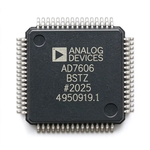
AD7606 - 16-Bit 8CH Simultaneous Sampling DAS | Analog Devices
AD7606

AD7606 - 16-Bit 8CH Simultaneous Sampling DAS | Analog Devices

The Analog Devices AD7606 is a 16-bit, 8-channel simultaneous sampling data acquisition system (DAS) that converts all eight inputs at throughput rates up to 200 kSPS while operating from a single 5 V supply and accepting true bipolar input ranges of ±10 V and ±5 V, housed in a 64-lead LQFP (10x10 mm) package. A data acquisition system (DAS) is an integrated circuit that combines signal conditioning, analog-to-digital conversion, and digital interface functions in one device. Within the converter hierarchy, the AD7606 belongs to the SAR (successive approximation register) ADC family, sits under analog-to-digital converters within the data converter / precision signal chain category, and functions as a complete power-management-friendly front end for industrial measurement systems. Key features include eight simultaneously sampled inputs, a fully integrated analog front end with input clamp protection that tolerates up to ±16.5 V at the pins, an on-chip input buffer with a 1 MΩ analog input impedance regardless of sampling frequency, and flexible digital interfaces (parallel, serial SPI, QSPI, and MICROWIRE) with a VDRIVE pin operating from 2.3 V to 5 V for direct connection to low-voltage DSPs and microcontrollers. Technically, the device employs a high-speed, low-power, charge-redistribution SAR ADC architecture with an on-chip antialiasing filter providing a 3 dB cutoff of 22 kHz and 40 dB antialias rejection when sampling at 200 kSPS. A pin-driven digital oversampling filter improves SNR and reduces signal bandwidth without host intervention. Single-supply 5 V operation plus bipolar input tolerance eliminates the need for external dual supplies, level shifters, or driver amplifiers. Typical applications include industrial motor-control and power-line monitoring, three-phase inverter and grid-quality measurement, and medical or scientific multi-channel data acquisition where true bipolar sensors must be sampled simultaneously. A key design consideration is that all eight channels share one 200 kSPS conversion cycle; the antialiasing filter bandwidth and oversampling ratio should be chosen together to balance noise against settling behavior at the input buffer. This page synthesizes distributor pricing, verified drop-in alternatives such as the AD7606B and GX7606, and practical design notes not found in the manufacturer datasheet.

RFQ Contact
AD7606BBCHIPS - 16-Bit 8-Ch 800kSPS DAS ADC | Analog Devices
AD7606BBCHIPS

AD7606BBCHIPS - 16-Bit 8-Ch 800kSPS DAS ADC | Analog Devices

The Analog Devices AD7606BBCHIPS is a 16-bit, simultaneous sampling, analog-to-digital data acquisition system (DAS) with eight channels, offering 800 kSPS throughput per channel with bipolar input capability. Each of the eight channels integrates analog input clamp protection, a programmable gain amplifier (PGA), a low-pass filter, and a 16-bit successive approximation register (SAR) analog-to-digital converter, all on a single die. A data acquisition system (DAS) is a signal-chain subsystem that converts real-world analog signals into digital data for processing. Within the ADC hierarchy, the AD7606BBCHIPS sits in the simultaneous-sampling SAR ADC family, which is preferred over multiplexed architectures when multiple channels must be sampled at exactly the same instant, such as in three-phase power measurement. Key features include true bipolar input operation from a single supply, an on-chip antialiasing filter with digitally programmable bandwidth, and a 5 MΩ analog input impedance. The high input impedance results in less than 20 LSB bipolar zero code error when an input is disconnected and pulled to ground through a 10 kΩ external resistor, eliminating the need for external bipolar-supply driver op amps. Architecturally, the AD7606BBCHIPS uses per-channel signal chains with integrated clamp protection, allowing direct connection to sensors and transformers while tolerating overvoltage faults. According to the ADI application note AN-1559, the AD7606B generation is a drop-in upgrade from the original AD7606 with higher input impedance, faster throughput, and extended temperature range. Typical applications include power line monitoring and protective relays, three-phase motor and inverter control, industrial automation DAQ modules, and medical instrumentation. The 800 kSPS simultaneous sampling across all eight channels makes it well suited to power quality analyzers and grid monitoring equipment. A key design consideration is that higher on-chip input impedance allows reduced-power signal sourcing, but the digital interface (parallel or serial SPI) must respect throughput timing when running at full 800 kSPS across all channels. Supply sequencing of the analog and digital rails should follow the datasheet power-up order. This page synthesizes distributor pricing, drop-in alternatives, and practical design notes not found in the manufacturer datasheet, verified as of 2026-09-14.

RFQ Contact
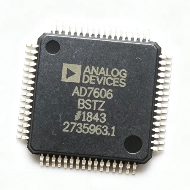
AD7606BSTZ - 16-Bit 8-Ch 200kSPS Simultaneous DAS ADC | Analog Devices
AD7606BSTZ

AD7606BSTZ - 16-Bit 8-Ch 200kSPS Simultaneous DAS ADC | Analog Devices

The Analog Devices AD7606BSTZ is a 16-bit, 8-channel, simultaneous-sampling data acquisition system (DAS) housed in a 64-lead LQFP (10x10 mm) package. It integrates analog input clamp protection, a second-order antialiasing filter, a track-and-hold amplifier, a 16-bit charge-redistribution successive-approximation ADC, a 2.5V on-chip reference and reference buffer, and high-speed serial and parallel interfaces. The device accepts true bipolar input ranges of ±10V or ±5V and runs from a single 5V analog supply, with a separate 2.3V-to-5V VDRIVE rail for the digital host interface. Throughput is 200 kSPS per channel, with all eight channels sampled at the same instant on the rising edge of CONVST. A Data Acquisition System (DAS) is a complete mixed-signal front-end that conditions, samples, and digitizes multiple analog signals for a downstream host processor. The AD7606BSTZ sits in the family of simultaneous-sampling ADCs - between analog sensors and a DSP, FPGA, or microcontroller - and is a member of the broader converter hierarchy: ADC -> data converter -> mixed-signal IC -> semiconductor. Simultaneous-sampling DA conversion preserves the phase relationship between channels, a property that single-channel sequentially-sampling ADCs cannot deliver. Key differentiating features include eight truly simultaneous track-and-hold channels, on-chip oversampling digital filter with 2x/4x/8x/16x/32x/64x ratios, integrated 2.5V reference with 10 ppm/°C drift, 1 MΩ analog input impedance that removes the need for external driver op-amps, and parallel/serial/SPI/QSPI/MICROWIRE-compatible digital I/O. Hardware-mode operation lets a host start conversions without writing any registers, useful for deterministic, low-latency control loops. Technically, the ADC core is a charge-redistribution SAR converter followed by a flexible digital filter. The analog front end combines ±25V tolerant input clamps, a 1 MΩ input buffer, and a second-order Butterworth antialiasing filter with a -3 dB corner near 22 kHz at 200 kSPS. The integrated reference can be overdriven by an external low-impedance source when tighter accuracy is needed. Power consumption is approximately 215 mW when all eight channels sample at 200 kSPS from ±10V inputs. Typical uses are three-phase power-line monitoring and protective relays (where phase-angle accuracy between voltage and current is critical), industrial motor control feedback, multi-axis vibration and modal analysis, and medical instrumentation. The bipolar ±10V/±5V ranges interface directly to current shunts and resistor-divider voltage networks, eliminating external signal conditioning. The eight-channel count suits four-quadrant power analyzers and multi-axis sensor pods without requiring an external mux. When designing with this device, place 10 µF + 0.1 µF decoupling capacitors close to each AVCC pin and a single 10 µF + 0.1 µF pair on VDRIVE. Drive CONVSTA and CONVSTB simultaneously to guarantee true simultaneous sampling across all eight channels. If higher DC accuracy is required, drive REFIN/REFOUT from an external low-impedance reference rather than using the internal 2.5V source. This page synthesizes distributor pricing, drop-in alternatives, and practical design notes not found in the manufacturer datasheet - useful for engineers qualifying second sources or planning migrations to the newer AD7606B family.

USD $20.85 In Stock
AD7606BSTZ - 16-Bit 8-Ch Simultaneous ADC | Analog Devices
AD7606BSTZ

AD7606BSTZ - 16-Bit 8-Ch Simultaneous ADC | Analog Devices

The AD7606BSTZ is a 16-bit, 8-channel, simultaneous sampling analog-to-digital data acquisition system (DAS) from Analog Devices. It integrates analog input clamp protection, a second-order antialiasing filter, a track-and-hold amplifier, a 16-bit charge redistribution successive approximation ADC, a flexible digital filter, a 2.5V reference and reference buffer, and high-speed serial and parallel interfaces. The device operates from a single 5V supply and accepts bipolar input ranges of ±5V and ±10V, making it ideal for power-line monitoring and industrial data acquisition. A data acquisition system (DAS) is a complete signal chain that conditions, samples, and digitizes analog signals. The AD7606BSTZ belongs to the family of simultaneous sampling ADCs, which capture multiple channels at the same instant, preserving phase relationships critical for power metering and vibration analysis. It sits between analog sensors and a digital host processor, converting real-world signals into digital words for processing. Key features include 16-bit resolution, 200 kSPS throughput per channel, 8 simultaneous sampling channels, and a 64-lead LQFP package. The device offers a parallel, serial, SPI, QSPI, and MICROWIRE interface, providing flexibility for various host controllers. The integrated 2.5V reference and buffer eliminate the need for external reference components, simplifying design and reducing BOM cost. Technically, the AD7606BSTZ uses a successive approximation register (SAR) architecture with a charge redistribution DAC. The analog front end includes a second-order antialiasing filter with a cutoff frequency of 22 kHz, which attenuates out-of-band noise. The digital filter provides programmable oversampling ratios to further reduce noise. The device operates over the industrial temperature range of -40°C to +85°C and is available in a 10x10 mm LQFP package. Typical applications include power-line monitoring, protective relays, motor control, and multi-axis vibration analysis. The simultaneous sampling capability ensures accurate phase measurement between voltage and current channels, which is essential for power quality analysis. The high input impedance and integrated protection make it robust for harsh industrial environments. When designing with the AD7606BSTZ, ensure proper decoupling of the AVCC and DVCC supplies with 10 µF and 0.1 µF capacitors placed close to the pins. The REFIN/REFOUT pin can be driven by an external reference if higher accuracy is required, but the internal 2.5V reference is sufficient for most applications. The CONVST pins should be driven simultaneously to achieve true simultaneous sampling.

USD $16.90 Contact
AD7606BSTZ-4 - 16-Bit 4-Ch Simultaneous Sampling ADC | Analog Devices
AD7606BSTZ-4

AD7606BSTZ-4 - 16-Bit 4-Ch Simultaneous Sampling ADC | Analog Devices

The AD7606BSTZ-4 from Analog Devices is a 16-bit, 4-channel simultaneous sampling analog-to-digital data acquisition system (DAS) in a 64-lead LQFP (10x10 mm) package. It operates from a single 5 V supply and accommodates true bipolar input signals of ±10 V and ±5 V while sampling at throughput rates up to 200 kSPS for all channels. The device integrates analog input clamp protection, a second-order antialiasing filter, a track-and-hold amplifier, a 16-bit charge redistribution successive approximation ADC, a flexible digital filter, a 2.5 V reference, and reference buffer. The AD7606BSTZ-4 supports multiple serial interface modes including DSP, MICROWIRE, QSPI, and SPI, as well as a parallel interface, making it versatile for various microcontroller and DSP connections. A data acquisition system (DAS) is a complete signal chain that conditions, samples, and converts analog signals into digital data for processing. The AD7606BSTZ-4 integrates the entire front-end, eliminating the need for external op-amps, filters, and references, which simplifies design and reduces board space. As a simultaneous sampling ADC, it captures all four channels at the same instant, which is critical for applications requiring phase-accurate measurements across multiple inputs, such as power monitoring and motor control. Key features include 1 MΩ analog input impedance regardless of sampling frequency, input clamp protection up to ±16.5 V, and a 3 dB cutoff frequency of 22 kHz for the antialiasing filter, providing 40 dB antialias rejection at 200 kSPS. The flexible digital filter is pin-driven, yielding improvements in SNR and reducing the 3 dB bandwidth. The device operates over the industrial temperature range of -40°C to +85°C and is RoHS compliant. The AD7606BSTZ-4 uses a charge redistribution successive approximation architecture, which offers excellent DC accuracy and low power consumption. The integrated 2.5 V reference and buffer ensure stable conversion results without external components. The device also features a flexible digital filter that can be configured via the oversampling pins to trade off throughput for noise performance, allowing designers to optimize SNR for their specific application. Typical applications include power line monitoring, protective relays, motor control, and industrial data acquisition systems. The simultaneous sampling capability and high input impedance make it ideal for measuring three-phase voltages and currents with phase accuracy. The wide input range and clamp protection ensure robust operation in harsh industrial environments. When designing with the AD7606BSTZ-4, ensure that the analog input signals are within the specified ±10 V or ±5 V ranges and that the supply decoupling is adequate. The device requires a clean 5 V supply and proper grounding to achieve the specified performance. The digital interface should be configured according to the host processor's requirements, and the oversampling pins should be set to achieve the desired balance between throughput and noise.

RFQ Contact
AD7606BSTZ-4RL - 4Ch 16-Bit 200kSPS ADC DAS | Analog Devices
AD7606BSTZ-4RL

AD7606BSTZ-4RL - 4Ch 16-Bit 200kSPS ADC DAS | Analog Devices

The AD7606BSTZ-4RL is a 4-channel, 16-bit, simultaneous sampling analog-to-digital data acquisition system (DAS) from Analog Devices, packaged in a 64-lead LQFP (10x10 mm). It integrates analog input clamp protection, a second-order antialiasing filter, a track-and-hold amplifier, a 16-bit charge redistribution successive approximation ADC, a flexible digital filter, a 2.5V reference, and reference buffer, all on a single chip. Operating from a single 5V analog supply and a 2.3V to 5V VDRIVE interface supply, it supports true bipolar input ranges of ±10V and ±5V, making it ideal for industrial power monitoring, motor control, and data acquisition systems. A data acquisition system (DAS) is a complete signal chain that conditions, samples, and converts analog signals into digital data for processing. The AD7606BSTZ-4RL belongs to the family of simultaneous sampling ADCs, which capture multiple channels at the exact same instant, preserving phase relationships critical for applications like three-phase power analysis. As a DAS, it integrates front-end protection, filtering, and conversion, reducing external component count versus discrete ADC implementations. Key features include 16-bit resolution with 200 kSPS throughput on all channels, 95.5 dB SNR, and a flexible digital filter that improves noise performance. The device offers parallel, serial SPI, QSPI, MICROWIRE, and DSP-compatible interface options. The on-chip 2.5V reference and buffer eliminate external reference components, while the 1 MΩ analog input impedance simplifies driver design. Technically, the AD7606BSTZ-4RL uses a successive approximation register (SAR) architecture with charge redistribution, achieving high accuracy and low power. The integrated second-order antialiasing filter simplifies external filtering, and input clamp protection handles overvoltage up to ±16.5V. The device operates over the industrial temperature range of -40°C to +85°C. Typical applications include power line monitoring, motor control, industrial automation, and test and measurement equipment. Its simultaneous sampling capability is essential for accurate phase measurement in polyphase power systems, while high input impedance and integrated protection make it robust for direct sensor interfacing. When designing with this device, ensure proper decoupling of AVCC and VDRIVE supplies, and tune the digital filter settings to balance noise versus throughput. Careful PCB layout is needed to minimize digital noise coupling into the analog inputs.

RFQ Contact