Interface ICs
Subcategories
Products (181)

AD5700-1ACPZ - HART FSK Modem IC | Analog Devices
The AD5700-1ACPZ is a single-chip HART FSK half-duplex modem from Analog Devices, designed to comply with the HART physical layer requirements. It integrates all necessary filtering, signal detection, modulation, demodulation, and signal generation functions, requiring few external components. The device operates over a supply voltage range of 2.7V to 5.5V and is available in a 24-lead LFCSP-WQ (4x4 mm) package. It features a maximum supply current of 115 µA, making it ideal for loop-powered applications. The AD5700-1 variant includes an integrated 0.5% precision oscillator, saving board space and external component count. A HART modem is a specialized integrated circuit that enables digital communication over analog 4-20 mA current loops, commonly used in industrial process automation. It modulates and demodulates Frequency Shift Keying (FSK) signals at 1200 Hz and 2200 Hz, allowing digital data to be superimposed on the analog signal without interference. The HART protocol is a hybrid analog/digital standard widely adopted in smart transmitters, actuators, and control systems. The AD5700-1ACPZ belongs to the category of communication ICs, specifically modems, and is a key component in industrial communication systems. Key features include a 0.5% precision oscillator, low power consumption of 115 µA, and compliance with HART physical layer specifications. The device supports both master and slave configurations, making it versatile for various applications. It also includes an internal voltage reference and a carrier detect output, simplifying system design. The operating temperature range is -40°C to +125°C, suitable for harsh industrial environments. Technically, the AD5700-1 uses a digital signal processing architecture to achieve reliable FSK modulation and demodulation. The integrated oscillator eliminates the need for an external crystal, reducing component count and board space. The device also features a UART interface for easy connection to microcontrollers. The LFCSP package provides excellent thermal performance and a compact footprint, ideal for space-constrained designs. Typical applications include smart transmitters, process control systems, field instruments, and HART-based communication interfaces. The low power consumption and integrated oscillator make it particularly suitable for loop-powered devices where power is limited. The device is also used in HART master systems, such as handheld communicators and control room equipment. When designing with the AD5700-1ACPZ, ensure proper decoupling of the power supply and careful layout of the analog front-end to minimize noise. The device requires a few external components, including a coupling capacitor and a protection circuit for the HART signal path. Refer to the datasheet for recommended application circuits and layout guidelines.
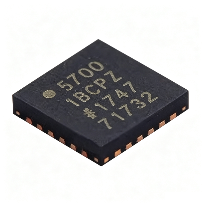
AD5700-1BCPZ - HART FSK Modem IC | Analog Devices
The AD5700-1BCPZ is a single-chip HART FSK half-duplex modem from Analog Devices, designed to comply with the HART physical layer requirements. It integrates all necessary filtering, signal detection, modulation, demodulation, and signal generation functions, requiring few external components. The device operates from a 2.7V to 5.5V supply and features an internal oscillator, eliminating the need for an external crystal. It is available in a compact 24-lead LFCSP-WQ (4x4 mm) package, making it ideal for space-constrained industrial applications. A HART modem is a specialized integrated circuit that enables communication over legacy 4-20 mA analog loops by superimposing a digital frequency-shift keying (FSK) signal. The HART protocol uses two frequencies: 1200 Hz for logic '1' and 2200 Hz for logic '0', allowing simultaneous analog and digital communication. The AD5700-1BCPZ is part of the HART modem product family, which falls under the broader category of industrial communication ICs, specifically interface ICs for process automation. Key features of the AD5700-1BCPZ include a low power consumption of 1 mA typical, an integrated receive band-pass filter that can be bypassed, and an internally buffered HART output with high drive capability. The device also includes an internal 2.5V reference and supports a wide operating temperature range of -40°C to +125°C. The LFCSP package provides excellent thermal performance and a small footprint, suitable for high-density designs. Technically, the AD5700-1BCPZ uses a digital signal processing (DSP) architecture to implement the HART modem functions, ensuring accurate and reliable communication. The integrated filter eliminates the need for external components, simplifying the design and reducing bill of materials cost. The device is fully compliant with the HART physical layer specification, ensuring interoperability with other HART-compliant devices. Typical applications include industrial process control, smart transmitters, valve positioners, and other field instruments that require HART communication. The low power consumption and small package make it suitable for loop-powered devices where power budget is critical. The internal oscillator further reduces component count, making it an excellent choice for compact designs. When designing with the AD5700-1BCPZ, ensure proper decoupling of the power supply and careful layout of the analog and digital sections to minimize noise. The device requires a few external components, including a coupling capacitor and a protection circuit for the HART signal path. Refer to the datasheet for detailed application circuits and recommended component values.
AD5700-1BCPZ-RL - HART Modem IC with Oscillator | Analog Devices
The AD5700-1BCPZ-RL is a single-chip HART FSK half-duplex modem from Analog Devices, designed to comply with the HART physical layer requirements. It integrates all necessary filtering, signal detection, modulation, demodulation, and signal generation functions, requiring few external components. The device operates from a 2.7V to 5.5V supply and features an integrated oscillator, eliminating the need for an external crystal. It is available in a compact 24-lead LFCSP-WQ (4x4 mm) package, suitable for space-constrained industrial applications. A HART modem is a specialized integrated circuit that enables communication over legacy 4-20 mA analog loops by superimposing a frequency-shift keying (FSK) digital signal. The AD5700-1 is part of the HART modem product family, which falls under the broader category of industrial communication ICs. These devices are essential in process automation, allowing digital configuration and diagnostics without disrupting analog measurement signals. Key features include a low-power design with a typical supply current of 86 µA in listen-only mode, an integrated receive band-pass filter that can be bypassed, and an internally buffered HART output for high drive capability. The device also includes an internal reference, a RESET pin for power-down mode, and a REF_EN pin to control the internal reference. The integrated oscillator provides a precise 1.2 MHz clock, simplifying the design and reducing component count. The AD5700-1 uses a digital signal processing (DSP) architecture to implement the HART protocol, ensuring reliable communication over long cable runs. The device supports data rates of 1200 bps, the standard HART speed, and is fully compliant with the HART physical layer specification. The LFCSP package offers excellent thermal performance and a small footprint, making it ideal for loop-powered transmitters and other compact field instruments. Typical applications include industrial process control, smart transmitters, valve positioners, and other field instruments that require HART communication. The device interfaces easily with Analog Devices' industrial converters, such as the AD5421 loop-powered current-output DAC, enabling complete smart transmitter solutions. When designing with the AD5700-1, ensure proper decoupling on the supply pins and follow the recommended layout in the datasheet to minimize noise. The RESET pin can be used to place the device in power-down mode, reducing current consumption to 1 µA, which is critical for loop-powered applications.
AD5700-1BCPZ-RL7 - Low Power HART Modem | Analog Devices
The AD5700-1BCPZ-RL7 is a single-chip HART FSK half-duplex modem from Analog Devices, designed to meet HART physical layer requirements for industrial field instrumentation. Housed in a 24-LFCSP-WQ (4x4) package, this low-power modem operates from a 1.71 V to 5.5 V supply and draws a maximum of 115 µA in receive mode, making it suitable for loop-powered and intrinsically safe applications. The AD5700-1 variant integrates a precision internal oscillator, eliminating the need for an external crystal and reducing component count and board area. A HART modem is a communication IC that superimposes digital Frequency Shift Keying (FSK) signals onto a 4-20 mA analog current loop, using 1200 Hz and 2200 Hz sinusoidal tones to represent logic '1' and logic '0'. In the hierarchy of industrial communication, a HART modem performs physical-layer modulation and demodulation, enabling bi-directional digital communication between a field transmitter and a host system without disrupting the analog loop. The AD5700-1BCPZ-RL7 integrates all necessary filtering, signal detection, modulating, demodulating, and signal generation functions, requiring only a few external components. Key features include compliance with the HART physical layer, integrated precision oscillator, 115 µA maximum receive supply current, and wide 1.71 V to 5.5 V operating range. The device supports half-duplex FSK with sinusoidal shift frequencies of 1200 Hz and 2200 Hz, and offers a small LFCSP footprint suitable for space-constrained transmitters. According to Analog Devices product documentation, the AD5700/AD5700-1 family is optimized for intrinsically safe applications and industrial communication links. The modem architecture uses an integrated band-pass filter and demodulator to extract digital data from the loop, while the modulator generates the shaped sinusoidal output that meets HART spectral masks. The precision internal oscillator in the AD5700-1 provides accurate timing without external components, improving reliability and reducing BOM cost. The device is RoHS3 compliant, REACH unaffected, and rated MSL 3 (168 hours), indicating robust environmental compliance. Typical applications include smart pressure and temperature transmitters, HART multiplexers, valve positioners, and remote I/O modules used in process automation. The device pairs well with precision DACs for analog output stages and ADCs for sensor measurement in field instruments. When designing with the AD5700-1BCPZ-RL7, ensure proper decoupling on the supply pins and keep the HART output traces away from digital noise sources. Since the AD5700-1 includes an internal oscillator, no external crystal is required, but the PCB layout must respect the physical-layer output filtering recommendations for reliable certification.
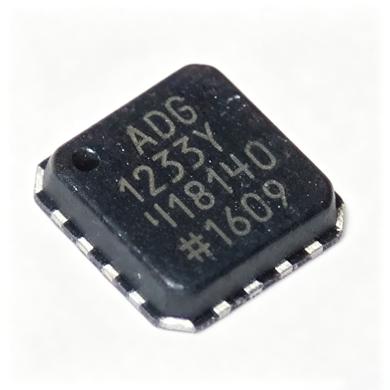
ADG1233YCPZ-REEL7 - Triple SPDT Analog Switch | Analog Devices
The ADG1233YCPZ-REEL7 is a monolithic iCMOS® analog switch from Analog Devices, integrating three independently selectable single-pole, double-throw (SPDT) switches in a compact 16-lead LFCSP-VQ (4x4 mm) package. It operates over a wide supply range of ±15 V or +12 V, with a low on-resistance of 120 Ω (typical) and ultra-low capacitance of 1.5 pF off capacitance, making it ideal for high-performance signal routing in precision instrumentation, audio, and data acquisition systems. An analog switch is a semiconductor device that selectively connects or disconnects an analog signal path under digital control. It is a fundamental building block in signal routing, multiplexing, and sample-and-hold circuits. The ADG1233 belongs to the family of analog switches and multiplexers, which are part of the broader category of interface ICs and signal conditioning components. Its iCMOS® (industrial CMOS) process technology ensures low power consumption and high voltage handling, bridging the gap between traditional CMOS and higher-voltage bipolar processes. Key features include break-before-make switching action, which prevents momentary shorting when switching channels, and an EN input that enables or disables the entire device. The switch is fully specified with 3 V logic-compatible inputs, allowing direct interface with low-voltage digital controllers. Rail-to-rail operation ensures minimal signal distortion across the full supply range. The 1.5 pF off capacitance and 0.5 pC charge injection minimize signal degradation in high-frequency and precision applications. The ADG1233 utilizes a proprietary iCMOS® process that combines the advantages of high-voltage CMOS with low power dissipation. This architecture enables the device to handle ±15 V supplies while maintaining low leakage currents and fast switching speeds. The break-before-make action is implemented through internal timing circuitry, ensuring reliable channel isolation during transitions. The device is available in a 16-lead LFCSP-VQ package, which offers excellent thermal performance and a small footprint for space-constrained designs. Typical applications include audio signal routing, precision data acquisition systems, automatic test equipment (ATE), and medical instrumentation. The low capacitance and charge injection make it particularly suitable for high-speed analog signals, while the wide supply range accommodates both bipolar and single-supply designs. The EN pin provides a convenient means of power-down or signal isolation in multi-channel systems. When designing with the ADG1233, ensure that the digital control signals are within the specified logic thresholds and that the supply voltages are properly decoupled with 0.1 µF capacitors close to the VDD and VSS pins. The break-before-make feature eliminates the need for external timing circuits, but the user should verify that the switching time meets system requirements.

ADG1236YCPZ-500RL7 - Dual SPDT ±15V iCMOS Analog Switch | ADI
The Analog Devices ADG1236YCPZ-500RL7 is a low-capacitance, low-charge-injection dual SPDT (single-pole double-throw) analog switch fabricated on the iCMOS process, offering a 33 V supply range, 1 pC charge injection, and 1.3 pF off capacitance in a 12-lead LFCSP (3 mm x 3 mm) package. An analog switch is an electronic component that routes or blocks analog signal paths under digital control. Within the signal-chain hierarchy, it belongs to the multiplexer/switch family of interface ICs, sitting between sensors or signal sources and amplifiers, ADCs, or measurement front ends. SPDT switches route one common terminal to one of two throw terminals, enabling source selection, gain-range switching, and redundant-path switchover in precision systems. Key features include 1.3 pF off capacitance and 3.5 pF on capacitance, which minimize signal distortion in high-frequency and capacitive-sensitive nodes, and 1 pC charge injection that reduces glitches when switching precision sample-and-hold or integrator circuits. The 33 V supply range supports +/-15 V dual-supply and 12 V single-supply operation, and the iCMOS process combines high-voltage CMOS and bipolar technologies for industrial-grade robustness. Logic inputs are 3 V logic-compatible and no VL supply pin is required, simplifying interfacing with low-voltage controllers. Technically, the iCMOS process allows high-voltage analog handling with low-voltage digital control, so the switch blocks up to +/-15 V signals while the control logic accepts standard 3.3 V or 5 V levels. The monolithic CMOS construction ensures low power and matched switch behavior across both SPDT channels, which switch independently for flexible routing. Typical applications include automated test equipment (ATE) signal routing, data-acquisition channel selection, precision sample-and-hold circuits, and industrial instrumentation where large-swing signals meet low-glitch switching requirements. Design consideration: on resistance is approximately 120 ohm typical (190 ohm maximum per DigiKey listing), so account for Ron flatness and voltage drop in high-impedance or precision-gain paths. This page synthesizes distributor pricing, drop-in alternative analysis, and practical design notes not found in the manufacturer datasheet, with data verified as of 2026-09-10.

ADG709BRUZ-REEL7 - 4:1 Differential MUX | Analog Devices
The ADG709BRUZ-REEL7 is a low voltage, CMOS analog multiplexer from Analog Devices, comprising four differential channels. It switches one of four differential inputs to a common differential output, controlled by a 2-bit binary address (A0, A1) and an enable (EN) input. When disabled, all channels are switched OFF. The device operates over a supply range of 1.8 V to 5.5 V, with a low on-resistance of 4.5 ohm, making it suitable for precision analog signal routing in battery-powered and low-voltage systems. An analog multiplexer is a device that selects one of several analog input signals and forwards it to a single output. In this case, the ADG709 is a differential 4:1 multiplexer, meaning it handles four differential signal pairs and routes one pair to the output. This is essential in applications where signal integrity and minimal distortion are critical, such as data acquisition systems, communication systems, and audio/video switching. The multiplexer acts as a switch, connecting the selected input to the output while providing high isolation from unselected channels. Key features of the ADG709BRUZ-REEL7 include bidirectional analog channels, glitch-free switching, and a wide operating temperature range of -40°C to +125°C. The low on-resistance of 4.5 ohm ensures minimal signal attenuation, while the CMOS construction provides low power consumption. The device is available in a 16-lead TSSOP package, which is compact and suitable for space-constrained designs. The EN pin allows for easy power-down or channel disabling, enhancing system flexibility. Technically, the ADG709 uses a CMOS process that provides low leakage currents and high switching speeds. The differential architecture improves noise immunity by rejecting common-mode noise, which is critical in industrial and communication environments. The device also features break-before-make switching, preventing momentary shorting of channels during transitions. This ensures glitch-free operation, which is vital in precision measurement and audio applications. Typical applications include data acquisition systems, communication systems, relay replacement, audio and video switching, and battery-powered systems. In data acquisition, the ADG709 can route multiple sensor signals to a single ADC, reducing component count and cost. In audio systems, it enables seamless switching between multiple audio sources without audible clicks or pops. When designing with the ADG709, ensure that the analog input signals remain within the supply rails to avoid forward-biasing the internal diodes. Additionally, proper decoupling of the power supply pins with 0.1 uF capacitors is recommended to minimize noise. The EN pin can be used to place the device in a low-power state when not in use, conserving battery life in portable applications.

ADM222ARZ - 2/2 RS-232 Transceiver 200kbps | Analog Devices
The ADM222ARZ is a high-speed, 5 V, 0.1 µF CMOS RS-232 transceiver from Analog Devices, featuring two drivers and two receivers in an 18-pin SOIC-W package. It operates from a single 5 V supply and uses an on-chip charge pump with small 0.1 µF external capacitors to generate RS-232 bipolar levels, achieving data rates up to 200 kbps. The device includes a shutdown (SHDN) pin that reduces supply current to 0.1 µA, making it ideal for power-sensitive portable applications. RS-232 transceivers are interface ICs that convert logic-level signals to RS-232 voltage levels for serial communication. They are part of the interface IC family, which also includes RS-485, CAN, and USB transceivers. The ADM222ARZ specifically provides the electrical signaling and protection required for legacy serial ports, enabling communication between microcontrollers and peripherals such as modems, GPS modules, and industrial equipment. Key features include a 200 kbps data rate, 0.1 µF charge pump capacitors, and a shutdown mode with 0.1 µA supply current. The device is fully compliant with EIA-232E standards and features a wide operating temperature range of -40°C to +85°C. The 18-pin SOIC-W package is suitable for space-constrained designs while providing adequate thermal performance. Technically, the ADM222ARZ uses a CMOS charge pump architecture to generate ±10 V RS-232 levels from a single 5 V supply. The internal charge pump requires only four external 0.1 µF capacitors, reducing board space and cost compared to older designs requiring larger capacitors. The receiver inputs tolerate up to ±30 V, providing robust protection against voltage spikes on the serial line. Typical applications include industrial automation, point-of-sale terminals, medical devices, and any system requiring reliable RS-232 communication. The shutdown feature is particularly useful in battery-powered devices where power conservation is critical. When designing with the ADM222ARZ, ensure that the charge pump capacitors are placed close to the V+ and V- pins to minimize noise and maintain proper voltage generation. The shutdown pin can be driven by a microcontroller GPIO to enter low-power mode when the serial port is idle.

ADM2485BRWZ - Isolated RS-485 Transceiver | Analog Devices
The ADM2485BRWZ is a high-speed, galvanically isolated RS-485/RS-422 transceiver with an integrated transformer driver, manufactured by Analog Devices. It is designed for bidirectional data communication on multipoint bus transmission lines and complies with ANSI/TIA/EIA RS-485-A-98 and ISO 8482:1987 (E). The device integrates a 3-channel digital isolator, a three-state differential line driver, and a differential input receiver, all in a 16-pin SOIC-W (wide body) package. It operates from a single 5V supply on the logic side and a 5V supply on the bus side, providing 2.5 kVrms isolation. The ADM2485BRWZ supports data rates up to 16 Mbps and features a high common-mode transient immunity (CMTI) of 25 kV/µs, making it suitable for industrial and harsh environments. A digital isolator is a component that provides galvanic isolation between two circuits while allowing digital signals to pass. It uses capacitive or magnetic coupling to transfer data across an isolation barrier, preventing ground loops and protecting sensitive electronics from high voltages. The ADM2485BRWZ uses Analog Devices' iCoupler technology, which combines high-speed CMOS and monolithic transformer technology to achieve reliable isolation. This places it in the category of interface ICs, specifically isolated RS-485 transceivers, which are essential in industrial automation, motor control, and building automation systems where noise immunity and safety are critical. Key features of the ADM2485BRWZ include a 16 Mbps data rate, 2.5 kVrms isolation voltage, 25 kV/µs CMTI, and an integrated transformer driver that simplifies the design of the isolated DC-DC converter. The device also has thermal shutdown protection and a wide operating temperature range of -40°C to +85°C. The receiver has a 1/8 unit load, allowing up to 256 nodes on the bus. The driver maintains a high output current of ±60 mA, ensuring robust signal integrity over long cable runs. The ADM2485BRWZ is designed for use in industrial networks, such as PROFIBUS, Modbus, and BACnet, where reliable data transmission over long distances is required. Its integrated transformer driver reduces external component count, saving board space and simplifying the power supply design. The device is available in a 16-pin SOIC-W package, which is suitable for surface-mount assembly and is RoHS compliant. When designing with the ADM2485BRWZ, it is important to ensure proper PCB layout to maintain isolation integrity. The isolation barrier should be kept clear of copper traces, and the transformer driver should be connected to a suitable external transformer and rectifier circuit to generate the isolated bus-side supply. Additionally, termination resistors should be placed at both ends of the bus to minimize reflections and ensure signal integrity.
ADM2485BRWZ-RL7 - Isolated RS-485 Transceiver | Analog Devices
The ADM2485BRWZ-RL7 is a high-speed, galvanically isolated RS-485/RS-422 transceiver with an integrated transformer driver, manufactured by Analog Devices. It combines a 3-channel digital isolator, a three-state differential line driver, and a differential input receiver into a single 16-pin SOIC-W package. The device supports data rates up to 16 Mbps and provides 2500 Vrms isolation, making it suitable for industrial networks, motor control, and building automation. A digital isolator is a component that provides electrical isolation between two circuits while allowing digital signals to pass. In the context of RS-485 communication, isolation protects against ground loops, common-mode voltage differences, and transient surges, ensuring reliable data transmission in harsh industrial environments. The ADM2485 uses Analog Devices' iCoupler technology, which uses chip-scale transformers instead of optocouplers, offering higher speed, lower power, and better reliability. Key features include a 3-channel isolator (one driver, one receiver, one data direction control), an integrated transformer driver that provides isolated power with an external transformer, and compliance with ANSI/TIA/EIA RS-485-A-98 and ISO 8482:1987(E). The device operates from a single 5V supply on the logic side and a 5V supply on the bus side, with a common-mode voltage range of -7V to +12V. It features thermal shutdown protection and a wide operating temperature range of -40°C to +85°C. The ADM2485 employs iCoupler technology, which uses chip-scale transformers to transmit data across an isolation barrier, providing superior performance compared to optocouplers. The integrated transformer driver generates a square wave that drives an external transformer to create an isolated power supply, eliminating the need for a separate DC-DC converter. This architecture reduces component count and board space while maintaining high isolation and data integrity. Typical applications include industrial fieldbus networks, PROFIBUS, Modbus, motor control, and building automation systems. The device is ideal for applications requiring robust communication over long distances in electrically noisy environments. Its high CMTI (25 kV/µs) ensures reliable operation in the presence of fast transients. When designing with the ADM2485, ensure proper PCB layout to maintain isolation creepage and clearance distances. Place the external transformer close to the device and use appropriate decoupling capacitors on both supply rails. The integrated transformer driver requires an external transformer with a 1:1 turns ratio and a center-tapped primary, as specified in the datasheet.
ADM2486BRWZ-RL7 - Isolated RS-485 Transceiver | Analog Devices
The Analog Devices ADM2486BRWZ-RL7 is a high-speed, half-duplex, galvanically isolated RS-485/RS-422 transceiver that delivers 2500 Vrms isolation, a 20 Mbps data rate, and 25 kV/µs common-mode transient immunity (CMTI). It is supplied in a 16-lead SOIC-W (16-SOIC, 7.50 mm body width) package on tape-and-reel (RL7 suffix), making it suitable for high-volume surface-mount assembly in industrial communication equipment. A digital isolator combined with an RS-485 transceiver is an integrated interface component that provides galvanic isolation between a logic-side controller and a high-voltage bus side. In a system hierarchy, the ADM2486 sits in the physical-layer interface between a UART, MCU, DSP, or PROFIBUS ASIC and the differential RS-485 bus. Its isolation barrier prevents ground loops, common-mode voltages, and transient noise from corrupting the logic-side supply and data lines, which is essential in industrial networking, factory automation, and building control. Key features include Analog Devices iCoupler® magnetic isolation technology, PROFIBUS compliance, ANSI EIA/TIA 485-A and ISO 8482:1987 (E) compliance, 20 Mbps data rate, 3 V operation on VDD1, and 25 kV/µs CMTI. The transceiver integrates a three-channel isolator, a three-state differential line driver, and a differential input receiver in one 16-SOICW package. The RL7 tape-and-reel packaging supports automated pick-and-place assembly, while the 16-pin SOIC wide-body footprint is a common industry-standard form factor. Technical depth is provided by the iCoupler architecture, which uses chip-scale transformers instead of optocouplers, offering better timing accuracy, longer life, and stable CMTI over temperature. The 25 kV/µs CMTI ensures that fast-rising common-mode transients generated by motor drives, inverters, and contactors do not produce bit errors on the bus. This makes the device well suited to electrically noisy industrial environments where isolation integrity is critical. Typical applications include PROFIBUS DP fieldbus networks, PLC remote I/O, motor-drive communication, building automation, smart-grid metering, and SCADA remote terminal units. With its 20 Mbps data rate, the ADM2486 supports both high-speed fieldbus traffic and slower legacy RS-485 systems, providing design flexibility across multiple product lines. When designing with this device, place the isolated bus-side components close to the field connector and maintain a clean isolation barrier on the PCB. Add 120 Ω termination resistors at both ends of the RS-485 bus and bias resistors if the receiver does not have integrated fail-safe biasing. The RL7 suffix denotes a 7-inch tape-and-reel package variant, so confirm reel quantity with the distributor for production planning.
ADM2491EBRWZ - Isolated RS-485 Transceiver | Analog Devices
The ADM2491EBRWZ from Analog Devices is a high-speed, ESD-protected, full-duplex isolated RS-485/RS-422 transceiver. It integrates an iCoupler® digital isolator and a differential line transceiver in a single 16-lead SOIC package, providing 5000 Vrms isolation and ±8 kV ESD protection on the RS-485 I/O pins. The device operates from a 5 V supply and supports data rates up to 16 Mbps, making it suitable for industrial fieldbus networks, motor control, and building automation systems. A digital isolator is a component that provides galvanic isolation between two circuits while allowing digital signals to pass. In the context of RS-485 communication, the ADM2491E isolates the bus side from the controller side, preventing ground loops and protecting sensitive electronics from high common-mode voltages. This isolation is critical in industrial environments where long cable runs and potential differences between nodes can cause data corruption or damage. Key features include a 25 kV/µs common-mode transient immunity (CMTI), which ensures reliable operation in noisy environments, and a wide operating temperature range of -40°C to +105°C. The device supports both half-duplex and full-duplex operation, with the transmitter outputs (Y, Z) and receiver inputs (A, B) configurable for either mode. The ADM2491E also features thermal shutdown protection and a logic-side supply voltage range of 3.0 V to 5.5 V, allowing interface with low-voltage controllers. The ADM2491E uses Analog Devices' iCoupler technology, which employs chip-scale transformers to achieve isolation, offering advantages over optocouplers in terms of speed, power consumption, and reliability. The device is fully specified over the industrial temperature range and is available in a lead-free, RoHS-compliant SOIC-16 package. Typical applications include industrial fieldbus networks (PROFIBUS, Modbus), motor control and drives, building automation (HVAC, lighting), and isolated data acquisition systems. The high CMTI and ESD protection make it ideal for harsh industrial environments where transient voltages are common. When designing with the ADM2491E, ensure proper PCB layout with adequate creepage and clearance distances for the isolation barrier. Place decoupling capacitors close to the VDD and VISO pins, and consider using a separate ground plane for the isolated side to minimize noise coupling.
ADM3050EBRWZ - 5.7kV Isolated CAN-FD Transceiver | Analog Devices
The ADM3050EBRWZ is a 5.7 kV rms isolated controller area network (CAN) physical layer transceiver from Analog Devices, designed for CAN and CAN FD applications. It integrates a 2-channel digital isolator and a CAN transceiver into a single 16-lead SOIC package using Analog Devices' iCoupler technology. The device fully meets the CAN flexible data rate (CAN FD) ISO 11898-2:2016 requirements and supports data rates up to 12 Mbps. A CAN transceiver is a physical layer device that connects a CAN controller to the differential bus lines (CANH and CANL). It converts the controller's logic-level signals to differential signals for transmission and vice versa for reception. In the system hierarchy, the ADM3050E sits between the CAN controller (often integrated in a microcontroller) and the twisted-pair bus, providing galvanic isolation to protect the controller and other low-voltage circuitry from high-voltage transients and ground potential differences. Key features include 5.7 kV rms isolation voltage, compliance with ISO 11898-2:2016, support for CAN FD data rates up to 12 Mbps, and a 5V supply voltage. The device is available in a 16-lead SOIC package (SOIC-16) and is RoHS compliant. It is designed for industrial automation, building control, and automotive applications where robust communication and isolation are critical. Technically, the ADM3050E uses iCoupler technology to combine isolation and transceiver functions, eliminating the need for external optocouplers and separate isolated power supplies. The device provides a fully isolated solution, with isolation between the CAN controller and the physical layer bus. It features a basic feature set, focusing on essential CAN communication without additional complexity. Typical applications include industrial fieldbus networks, motor control systems, HVAC control, and electric vehicle charging stations. The high isolation voltage and CAN FD support make it suitable for harsh environments where noise and ground loops are common. When designing with the ADM3050E, ensure proper PCB layout with adequate creepage and clearance distances for the isolation barrier. The device requires a 5V supply on both the logic side and the bus side, and external termination resistors may be needed depending on the bus configuration.

ADM3051BRWZ-RL7 - 5V ISO 11898 CAN Transceiver | ADI
ADM3051BRWZ-RL7 is an Analog Devices controller area network (CAN) physical layer transceiver that provides a robust interface between a CAN protocol controller and the two-wire CAN bus. It operates from a single 5 V VCC supply, complies with the ISO 11898 standard, and supports high-speed data rates up to 1 Mbps. The device is offered in an 8-lead SOIC package and is supplied in tape-and-reel packaging for high-volume assembly. What is a CAN transceiver? A controller area network (CAN) transceiver is an interface IC that converts logic-level signals from a CAN controller into the differential signals required on the CANH and CANL bus lines, and vice versa. It sits between the protocol controller and the physical twisted-pair bus, providing the required differential drive, receive sensitivity, and protection functions. In the system hierarchy, a CAN transceiver is part of the physical layer in a CAN network, below the data-link and application layers. The ADM3051 is a non-isolated, single-channel half-duplex transceiver intended for industrial and automotive networks where ISO 11898 compliant communication at up to 1 Mbps is required. Key features of ADM3051BRWZ-RL7 include short-circuit protection on CANH and CANL for shorts to power or ground in 24 V systems, operation with unpowered nodes that do not disturb the bus, and capability to connect 110 or more nodes. It also provides slope control on the RS pin to reduce radiated EMI, thermal shutdown protection, and a low-current standby mode for power-sensitive applications. These features make it a physically robust PHY for noisy or high-node-count environments. Technically, the ADM3051 is a CAN physical-layer IC in the Analog Devices ADM305x family. It uses a differential bus interface and includes bus fault protection and thermal shutdown in a single 8-pin SOIC package. The -RL7 suffix denotes 7-inch reel tape-and-reel packaging, and the BRWZ code indicates the lead-free (Z) SOIC (RW) package variant. The device is designed for 5 V-only systems, simplifying power supply design and enabling direct interface to 5 V CAN controllers without extra level shifting. Typical applications include industrial automation PLCs, automotive body electronic modules, building management system controllers, battery management systems, medical equipment and CAN data logging nodes. In each of these, the ADM3051's 1 Mbps speed, 110+ node bus capability, and short-circuit protection reduce risk of fieldbus faults while maintaining simple 5 V power architecture. When designing with ADM3051BRWZ-RL7, place a 120 ohm termination resistor between CANH and CANL at both ends of the bus and set the RS pin resistor to control the slew rate for EMI optimization. For best decoupling, use a 100 nF ceramic capacitor close to VCC and a bulk capacitor at the supply point.
ADM3052BRWZ-RL7 - Isolated CAN Transceiver 5kV | ADI
The Analog Devices ADM3052BRWZ-RL7 is an isolated Controller Area Network (CAN) physical layer transceiver with an integrated linear regulator, supplied in a 16-lead SOIC (SOIC-W) package on 7-inch tape and reel. It complies with ISO 11898 and uses Analog Devices iCoupler technology to combine a 3-channel digital isolator and a CAN transceiver in one package. The device supports data rates up to 1 Mbps and provides 5 kVrms signal isolation. An isolated CAN transceiver is an interface IC that places a galvanic isolation barrier between the logic-side CAN controller and the physical bus-side transceiver. In a CAN node, the controller sends TXD/RXD signals across the isolation barrier to the transceiver, which then drives the differential CANH and CANL bus lines. This prevents ground loops, common-mode voltages, and transient noise in industrial or automotive networks from disturbing the local microcontroller. The transceiver sits in the signal chain between the CAN controller and the twisted-pair bus, making isolation a key reliability requirement in harsh environments. Key features of the ADM3052 family include 5 kVrms isolation voltage, a 1/1 driver/receiver configuration, 1 Mbps ISO 11898-compliant data rate, and a logic-side supply of 3.3 V or 5 V. The integrated linear regulator enables bus-powered operation from a 24 V-class V+ rail, eliminating the need for a separate isolated DC-DC converter in many nodes. The 16-lead SOIC wide-body package supports surface-mount assembly and automated tape-and-reel production. From a design perspective, the ADM3052 integrates the isolation barrier, CAN transceiver, and LDO regulation into one package, simplifying PCB layout and reducing component count. The iCoupler technology provides common-mode transient immunity that is critical for reliable CAN communication in motor drives, battery packs, and factory-floor networks. Because the bus side can be powered directly from V+, the node can be designed as a two-wire bus-powered device in applications where a standalone isolated supply is not economically justified. Typical applications include automotive electronic control units, battery management systems, industrial CANopen networks, building automation, medical monitoring equipment, and test instrumentation. The combination of 5 kVrms isolation and bus-powered regulation makes the ADM3052 especially useful in distributed sensor nodes that must survive ground potential differences. When designing with this device, pay attention to the input voltage range and dropout of the integrated linear regulator, and place adequate bypass capacitance on the V+ and logic-side rails. The isolation barrier also requires proper PCB creepage and clearance to maintain the specified 5 kVrms withstand voltage.
ADM3202ARNZ-REEL - 3.3V RS-232 2/2 Transceiver | Analog Devices
The Analog Devices ADM3202ARNZ-REEL is a low-power, 2-driver/2-receiver RS-232 line transceiver that operates from a single +3.3 V supply, supports data rates up to 460 kbps, and uses four external 0.1 uF charge pump capacitors, housed in a 16-lead SOIC_N (3.90 mm width) package supplied on tape and reel. An RS-232 transceiver is an interface IC that converts logic-level UART signals (TTL/CMOS, typically 0 V to 3.3 V) into the wider voltage swings specified by the EIA-232E and CCITT V.28 standards, and vice versa. Within the signal chain hierarchy, it belongs to the transceiver class of drivers/receivers under Interface ICs, bridging microcontrollers, processors, or UARTs to legacy serial ports, industrial equipment, and point-of-sale hardware. Key features include single-supply 3.3 V operation with an on-chip charge pump voltage doubler/inverter, conformance to EIA-232E and V.28 specifications, high-speed operation up to 460 kbps, and small 0.1 uF external charge pump capacitors that reduce board area and bill-of-materials cost compared to older parts requiring 1 uF or larger capacitors. Technically, the ADM3202 integrates two charge pump stages (doubler and inverter) to generate approximately +/-6 V RS-232 rails from the 3.3 V supply. The drivers deliver guaranteed EIA-232E output levels, and the receivers include internal input pull-ups so that unconnected receiver inputs default to a known mark state. The ADM3202 variant has no shutdown pin; the related ADM3222 and ADM1385 add a low-power shutdown facility for battery applications. Typical applications include industrial equipment serial ports, embedded systems with RS-232 debug or console links, point-of-sale terminals, battery-powered portable instrumentation (with ADM3222 variants), and any 3.3 V microcontroller design interfacing to legacy RS-232 equipment. Design considerations: place the four 0.1 uF charge pump capacitors as close as possible to the device pins and observe datasheet polarity for the flying capacitors; ensure the supply can support the transient charge pump current during data transmission. This page synthesizes distributor pricing, drop-in alternatives, pinout, and practical design notes not found in a single manufacturer datasheet, as of 2026-09-13.
ADM3202ARNZ-REEL7 - 3.3V RS-232 2/2 Transceiver 460kbps | ADI
The Analog Devices ADM3202ARNZ-REEL7 is a low-power, 2-driver/2-receiver RS-232/V.28 line transceiver that operates from a single +3.3 V supply, supports data rates up to 460 kbps, and uses only four external 0.1 uF charge pump capacitors, housed in a 16-pin SOIC (0.154 in / 3.90 mm width) package supplied on tape and reel. An RS-232 transceiver is an interface IC that converts logic-level UART signals (TTL/CMOS, typically 0 V to 3.3 V) to the higher voltage swings defined by the EIA-232E and ITU V.28 standards, and vice versa. Within the signal-chain hierarchy, it belongs to the interface IC family alongside RS-485, CAN and USB transceivers, and sits between a microcontroller UART and a physical D-sub serial port. Because RS-232 rails can swing to +/-5 V or more, an integrated charge pump (voltage doubler and inverter) is required when only a single low-voltage supply is available. Key features of the ADM3202 include guaranteed 460 kbps operation for high-speed serial links, operation from a 3 V to 5.5 V supply range per distributor parametric data, EIA-232E/V.28 conformance, and a small external capacitor requirement of only 4 x 0.1 uF, which reduces board area and BOM cost. The complementary ADM3222/ADM1385 family members add a low-power shutdown facility for battery-powered portable instruments. Technically, the device uses CMOS charge-pump technology with integrated driver and receiver channels. The charge doubler generates V+ and the inverter generates V- from the 3.3 V rail, enabling true RS-232 output levels without a dual supply. Receivers incorporate hysteresis and tolerate input voltages up to +/-30 V, improving noise immunity on long cables. Typical applications include industrial point-of-sale equipment, networking and communication equipment serial management ports, embedded systems console/debug ports, and battery-powered portable instruments with RS-232 connectivity. Design considerations: place the four 0.1 uF charge pump capacitors as close as possible to pins 1-6, and use at least 0.1 uF of supply decoupling on VCC; note the ADM3202 itself lacks the shutdown pin available on the ADM3222 variant. This page synthesizes distributor availability, drop-in alternatives, pinout detail and design notes beyond what a single datasheet provides.

ADN4624BCPZ - Quad 2.5Gbps LVDS Isolator | Analog Devices
The ADN4624BCPZ is a quad-channel, signal-isolated, low-voltage differential signaling (LVDS) buffer from Analog Devices that operates at data rates up to 2.5 Gbps with very low jitter. It integrates Analog Devices' iCoupler technology, enhanced for high-speed operation, to provide drop-in galvanic isolation of LVDS signal chains. The device is available in a 32-lead WFQFN exposed pad package (LFCSP) and supports a wide supply range of 1.7 V to 1.9 V on both VDD1 and VDD2, with a typical supply of 1.8 V. It provides 5700 Vrms isolation voltage and a common-mode transient immunity (CMTI) of 40 kV/µs, making it suitable for industrial and medical applications where robust isolation is critical. A digital isolator is a device that transfers digital signals across an isolation barrier, typically using capacitive, inductive, or optical coupling, to protect sensitive circuitry from high voltages, ground loops, and noise. In the hierarchy of signal conditioning, a digital isolator sits between the digital signal source and the receiving logic, ensuring signal integrity and safety. The ADN4624BCPZ specifically isolates LVDS signals, which are differential, low-voltage, high-speed signals used in applications like data acquisition, industrial networking, and medical imaging. Key features of the ADN4624BCPZ include four isolated LVDS channels (4+0 configuration), a data rate of 2.5 Gbps per channel, and very low jitter, which is essential for high-speed serial links. The device also features a refresh mechanism that monitors input and output states to ensure they remain the same in the absence of data transitions, such as at power-on. The 1.8 V supplies for the LVDS and isolator circuits enable low power consumption while maintaining high-speed operation. Technically, the ADN4624BCPZ uses iCoupler technology, which employs chip-scale transformers to couple signals across the isolation barrier. This approach provides superior performance compared to optocouplers in terms of speed, power, and reliability. The device is designed to meet the stringent requirements of industrial automation, motor control, and medical equipment, where isolation and signal integrity are paramount. Typical applications include isolated LVDS interfaces in data acquisition systems, industrial fieldbus networks, and medical imaging equipment. The ADN4624BCPZ is also used in test and measurement instruments where high-speed data transfer with galvanic isolation is required. When designing with this device, ensure that the supply voltages are within the specified range and that proper decoupling capacitors are placed close to the VDD pins. The exposed pad should be soldered to the PCB ground plane for optimal thermal performance. Also, consider the CMTI rating when operating in environments with high voltage transients.
ADN4624BCPZ-RL7 - Quad LVDS Isolator 2.5Gbps | Analog Devices
The ADN4624BCPZ-RL7 is a quad-channel, signal-isolated, low-voltage differential signaling (LVDS) buffer from Analog Devices that operates at data rates up to 2.5 Gbps with very low jitter. It integrates Analog Devices' iCoupler technology, enhanced for high-speed operation to provide drop-in galvanic isolation of LVDS signal chains. The device is available in a 32-lead WFQFN exposed pad package (CSP) and provides 5.7 kV rms isolation voltage with a common-mode transient immunity (CMTI) of 40 kV/µs. A digital isolator is a component that provides galvanic isolation between two circuits while allowing digital signals to pass across the isolation barrier. In the hierarchy of isolation components, a digital isolator is a type of signal isolator, which falls under the broader category of isolation components used in power management and signal conditioning. The ADN4624 specifically isolates LVDS signals, which are differential, low-voltage, high-speed signals commonly used in high-speed data transmission. Key features include four isolated LVDS channels (4+0 configuration), support for 1.7 V to 1.9 V supply voltages on both sides (VDD1 and VDD2), and an operating temperature range of -40°C to +125°C. The device ensures very low jitter, making it suitable for high-speed serial links where signal integrity is critical. The 5.7 kV rms isolation rating provides robust protection against voltage transients and ground potential differences. Technically, the ADN4624 uses iCoupler technology, which employs chip-scale transformers to transmit data across the isolation barrier, offering advantages over optocouplers in terms of speed, power consumption, and reliability. The device supports AC coupling and/or level shifting to LVDS receivers and from LVDS drivers, simplifying interface design. The 32-lead WFQFN package with exposed pad aids in thermal management and is suitable for space-constrained applications. Typical applications include isolated high-speed data acquisition systems, industrial fieldbus interfaces, medical equipment requiring patient isolation, and communication backplanes. The device is ideal for systems where high-speed data must cross an isolation barrier without compromising signal integrity. When designing with the ADN4624, ensure proper PCB layout with adequate spacing for isolation, and place decoupling capacitors close to the VDD1 and VDD2 pins. The exposed pad should be connected to the appropriate ground plane for thermal performance.

ADUM1201ARZ - Dual 2500Vrms 1Mbps Isolator | Analog Devices
The ADUM1201ARZ is a dual-channel digital isolator from Analog Devices, Inc., based on the proprietary iCoupler technology. It provides 2500Vrms isolation with a data rate of 1Mbps and a common-mode transient immunity (CMTI) of 25kV/µs. The device is housed in an 8-pin SOIC (0.154", 3.90mm width) package, making it suitable for space-constrained applications. It operates with a supply voltage range of 3.0V to 5.5V on both sides, allowing flexible interfacing with different logic levels. A digital isolator is a component that provides electrical isolation between two circuits while allowing digital signals to pass across the isolation barrier. Unlike optocouplers, which use LEDs and photodiodes, iCoupler devices use monolithic transformers and high-speed CMOS to achieve isolation. This approach eliminates the uncertain current transfer ratios, nonlinear transfer functions, and temperature and lifetime effects associated with optocouplers. Digital isolators are essential in applications where ground potential differences, noise, or safety requirements demand galvanic isolation, such as in industrial automation, medical equipment, and communication systems. Key features of the ADUM1201ARZ include its dual-channel configuration with 1/1 channel directionality, meaning one channel transmits data in each direction. The device supports data rates up to 1Mbps, making it suitable for low-to-moderate speed communication interfaces like SPI, UART, and GPIO isolation. The 25kV/µs CMTI ensures reliable operation in noisy environments, preventing false triggering due to fast transients. The iCoupler technology also consumes significantly less power than optocouplers, with typical quiescent current in the microampere range. The ADUM1201ARZ features a patented refresh mechanism that ensures DC correctness in the absence of input logic transitions and during power-up/power-down conditions. This is critical for maintaining the integrity of static signals across the isolation barrier. The device is available in both standard and automotive-grade versions, with the ADUM1201W variants qualified for 125°C operation. The 8-pin SOIC package is widely used and easy to integrate into existing PCB designs. Typical applications include isolating SPI and UART interfaces in industrial control systems, providing isolation in medical monitoring equipment, and protecting sensitive electronics in communication infrastructure. The device is also used in power supply control and motor drive circuits where high-voltage transients are present. Its small footprint and low power consumption make it ideal for portable and battery-powered devices. When designing with the ADUM1201ARZ, it is important to ensure proper power supply decoupling on both sides of the isolation barrier. Place 0.1µF capacitors close to the VDD1 and VDD2 pins to minimize noise. Additionally, consider the maximum data rate and CMTI requirements of your application to ensure the device meets your performance needs.
ADUM1201ARZ-RL7 - Dual-Channel Digital Isolator 2500Vrms | Analog Devices
The Analog Devices ADUM1201ARZ-RL7 is a dual-channel digital isolator based on the proprietary iCoupler technology, providing 2500Vrms galvanic isolation with a 1Mbps data rate and 25kV/µs common-mode transient immunity (CMTI). It is housed in an 8-SOIC (0.154", 3.90mm width) package, operates over a 3.0V to 5.5V supply range on both sides, and is rated for -40°C to +125°C operation. A digital isolator is a component that transfers digital signals across a galvanic isolation barrier without allowing direct current flow. Unlike optocouplers, which use LEDs and photodiodes, iCoupler devices use monolithic transformers and high-speed CMOS to achieve higher data rates, lower power consumption, and more stable performance over temperature and lifetime. Digital isolators are essential in systems where ground potential differences, noise, or safety requirements demand isolation, such as in industrial automation, medical equipment, and data acquisition. Key features of the ADUM1201ARZ-RL7 include 1/1 channel directionality (one forward channel and one reverse channel), which is ideal for bidirectional communication. The device delivers 2500Vrms isolation voltage, 1Mbps data rate, and 25kV/µs CMTI, ensuring reliable operation in noisy environments. The wide supply range supports both 3.3V and 5V logic levels, and the typical quiescent current is only 1.3mA per channel, making it suitable for power-sensitive applications. Technically, the ADuM1201 combines high-speed CMOS and monolithic transformer isolation in an 8-lead SOIC package. This architecture eliminates the need for external drivers and discrete components, reducing board space and improving reliability. Unlike optocouplers, iCoupler technology does not suffer from current transfer ratio degradation, providing stable isolation performance throughout the product lifetime. Typical applications include industrial automation for isolating field buses and sensor interfaces, medical devices where patient safety requires galvanic isolation, and data acquisition systems to prevent ground loops and noise. It is also used in power supply control, motor drives, and communication interfaces. When designing with this device, place bypass capacitors close to the VDD1 and VDD2 pins and maintain proper PCB spacing across the isolation barrier to preserve creepage and clearance requirements. The high CMTI rating makes the part robust in fast-switching environments, but careful layout is still required to maximize isolation performance.
ADUM1201BRZ - 2-Ch Digital Isolator 10Mbps | Analog Devices
The ADUM1201BRZ is a dual-channel digital isolator from Analog Devices, based on the proprietary iCoupler technology. It provides 2500Vrms isolation with a data rate of 10Mbps and a common-mode transient immunity (CMTI) of 25kV/µs. The device is housed in an 8-pin SOIC (0.154", 3.90mm width) package, making it suitable for space-constrained applications. It operates over a supply voltage range of 2.7V to 5.5V on both sides, allowing flexible interfacing with different logic levels. A digital isolator is a component that provides electrical isolation between two circuits while allowing digital signals to pass across the isolation barrier. Unlike optocouplers, which use LEDs and photodiodes, iCoupler devices use monolithic transformers and high-speed CMOS, eliminating concerns about current transfer ratio (CTR) degradation, nonlinear transfer functions, and temperature/lifetime effects. This results in more stable performance and lower power consumption—iCoupler devices consume about one-tenth the power of comparable optocouplers. Key features of the ADUM1201BRZ include a bidirectional channel configuration (1/1 directionality), a maximum data rate of 10Mbps, and a CMTI of 25kV/µs, which ensures reliable operation in noisy industrial environments. The device also offers a wide operating temperature range of -40°C to +105°C, making it suitable for harsh applications. The SOIC-8 package is industry-standard, enabling easy PCB layout and drop-in replacement in many designs. Technically, the ADUM1201BRZ uses a 2.7V to 5.5V supply range on both VDD1 and VDD2, with a maximum quiescent current of 2.6mA per channel. The propagation delay is typically 50ns, and the pulse width distortion is 3ns, ensuring accurate signal transmission. The device is certified to UL1577, IEC 60747-5-5, and CSA standards, providing robust isolation ratings. Typical applications include industrial fieldbus isolation, motor drives, battery monitoring, hybrid electric vehicles, and digital isolation in power supplies. The ADUM1201BRZ is particularly well-suited for isolating SPI, UART, and other serial interfaces where high-speed data transfer and reliable isolation are required. When designing with this device, ensure that the bypass capacitors (0.1µF) are placed close to the VDD pins to minimize noise. Also, consider the maximum data rate and CMTI requirements of your application to ensure the device meets your performance needs.
ADUM1201BRZ-RL7 - Dual-Channel Digital Isolator | Analog Devices
The ADUM1201BRZ-RL7 is a dual-channel digital isolator from Analog Devices, based on the proprietary iCoupler technology. It provides galvanic isolation up to 2500Vrms, with a data rate of 10Mbps and a common-mode transient immunity (CMTI) of 25kV/µs. The device is housed in an 8-pin SOIC (0.154", 3.90mm width) package, making it suitable for space-constrained applications. Digital isolators are components that transfer digital signals across an isolation barrier, preventing DC current flow while allowing AC signals to pass. They are essential in systems where safety, noise immunity, or ground potential differences are concerns. The ADUM1201BRZ-RL7 uses monolithic transformer technology, which offers superior performance compared to traditional optocouplers, including higher data rates, lower power consumption, and better reliability. Key features of the ADUM1201BRZ-RL7 include its 1/1 channel directionality (one forward, one reverse), a wide supply voltage range of 3.0V to 5.5V, and a propagation delay of typically 50ns. The device also features a high CMTI of 25kV/µs, ensuring reliable operation in noisy industrial environments. Its low power consumption and small package make it ideal for battery-powered and portable applications. The ADUM1201BRZ-RL7 is designed using Analog Devices' iCoupler technology, which integrates micro-transformers and high-speed CMOS circuits on a single chip. This architecture eliminates the need for external components and provides a robust isolation solution. The device meets various safety standards, including DIN EN 60950, and is RoHS compliant. Typical applications include motor drives, battery monitors, hybrid electric vehicles, and digital fieldbus isolation. In motor drives, the isolator protects control circuits from high-voltage transients. In battery monitoring, it ensures safe communication between cells and the controller. The device's high CMTI and data rate make it suitable for industrial automation and communication interfaces. When designing with the ADUM1201BRZ-RL7, it is important to ensure proper PCB layout to maintain isolation performance. Keep the isolation barrier clear of copper traces and place decoupling capacitors close to the supply pins. Also, consider the propagation delay and timing requirements of your system to avoid data corruption.
ADUM1250ARZ - Hot Swappable Dual I2C Isolator | Analog Devices
The ADUM1250ARZ is a hot-swappable, dual-channel digital isolator from Analog Devices, specifically designed for bidirectional I2C communication. It provides 2500Vrms isolation with a data rate of 1Mbps and a common-mode transient immunity (CMTI) of 25kV/µs. The device is housed in an 8-lead SOIC package (0.154", 3.90mm width) and operates from a 3.0V to 5.5V supply, making it suitable for a wide range of isolated I2C applications. Digital isolators are components that transfer digital signals across an isolation barrier without a direct electrical connection, using capacitive, inductive, or optical coupling. They are essential in systems where safety, noise immunity, or ground potential differences require galvanic isolation. The ADUM1250ARZ uses Analog Devices' proprietary iCoupler chip-scale transformer technology, which offers advantages over traditional optocouplers, including higher data rates, lower power consumption, and better reliability. Key features of the ADUM1250ARZ include nonlatching, bidirectional communication channels that are compatible with I2C interfaces, eliminating the need to split I2C signals into separate transmit and receive lines. It supports hot-swap capability, allowing insertion or removal of boards without powering down the system. The device also features open-drain outputs with 30mA current sink capability, ensuring compatibility with standard I2C bus specifications. Technically, the ADUM1250ARZ provides two bidirectional channels, supporting a complete isolated I2C interface. It has a maximum data rate of 1Mbps, which is sufficient for standard and fast-mode I2C. The isolation barrier is rated at 2500Vrms, providing robust protection against voltage transients. The device operates over a temperature range of -40°C to +125°C, making it suitable for industrial environments. Typical applications include isolated I2C buses in industrial automation, medical equipment, power management systems, and communication interfaces. The ADUM1250ARZ is also used in hot-swap applications where boards need to be replaced without interrupting system operation. When designing with the ADUM1250ARZ, it is important to ensure proper decoupling of the power supply pins and to follow the recommended layout guidelines to maintain isolation performance. The device is RoHS compliant and available in tape and reel packaging.