Interface ICs
Subcategories
Products (3,400+)

AD720JP RGB to NTSC/PAL Encoder | Analog Devices
The Analog Devices AD720JP is an RGB-to-NTSC/PAL video encoder integrated circuit with a 28-pin PLCC package. It produces a composite video output and separate chrominance and luminance outputs for S-Video, supports selectable NTSC or PAL encoding modes, and is designed to drive 75-ohm reverse-terminated video loads. The device also requires no external filters or delay lines, simplifying RGB video encoding systems. An RGB video encoder is a specialized interface IC that converts separate red, green, and blue component signals into a composite analog video waveform accepted by NTSC or PAL displays. Within the product hierarchy, the AD720JP belongs to the video encoder and converter class, then the broader interface IC and signal-conversion categories. It sits between an RGB graphics source and legacy composite or S-Video equipment. The AD720JP's principal features include logic-selectable NTSC and PAL operation, automatic selection of the appropriate encoding mode, separate S-Video chrominance and luminance outputs, and direct drive capability for 75-ohm reverse-terminated loads. The integrated implementation eliminates the external filter and delay-line networks normally associated with discrete RGB-to-composite encoding circuits. Its 28-pin PLCC package provides a compact surface-mount solution for industrial video, broadcast, control-panel, and embedded display equipment. Technically, the encoder organizes RGB component information into a composite color signal while providing separate Y and C outputs for S-Video equipment. Composite output and S-Video can therefore be used in the same design without duplicating the source RGB interface. Logic-selectable encoding allows one board design to support multiple regional video standards, while automatic mode selection can reduce operator configuration where an appropriate control signal is available. Typical applications include industrial monitoring panels, professional video equipment, broadcast-system interfaces, image-processing subsystems, video test equipment, and legacy display controllers that require conversion from RGB component video to NTSC or PAL. In each case, the device is most useful where compactness, integrated filtering, and direct 75-ohm loading are more important than the low latency of a software-based video pipeline. For a robust implementation, route the composite and S-Video outputs with controlled impedance and provide the termination network required by the target video standard. Keep sensitive analog routing away from switching nodes and use a stable ground reference between the encoder and the video connector. Confirm the selected encoding mode, electrical levels, and termination arrangement against the Analog Devices datasheet before releasing the production layout. This product page combines the AD720JP's confirmed encoding capabilities with application guidance, design cautions, comparison data, and documented procurement information. It helps engineers evaluate the 28-pin PLCC device for compact RGB-to-NTSC/PAL conversion while keeping package, output-routing, and video-standard decisions explicit.
AD721JP RGB to NTSC/PAL Encoder | Analog Devices
Analog Devices AD721JP is an RGB-to-NTSC/PAL color-signal encoder integrated circuit operating from ±5 V supplies and housed in a 28-pin plastic leaded chip carrier package. It generates composite video together with separate chrominance and luminance outputs for S-Video, drives 75-ohm reverse-terminated loads, and requires no external filters or delay lines. Its selectable encoding modes automatically configure the device for the appropriate NTSC or PAL timing convention. An RGB-to-NTSC/PAL encoder is a video-signal conversion IC that accepts red, green, and blue analog color components and combines them into a standard composite television signal. Within the broader signal-processing hierarchy, the AD721JP belongs to the color-signal encoder class, which supports display, broadcast, video-production, image-capture, and industrial monitoring systems. Separate S-Video outputs retain chrominance and luminance as independent signals, while the composite output combines the three RGB input channels for conventional video connections. Key features include logic-selectable NTSC and PAL encoding modes, a composite video output, individual chrominance and luminance outputs, and no requirement for external filters or delay lines. Its ability to drive 75-ohm reverse-terminated loads simplifies analog video output design because downstream cable and video-circuit impedances are matched at the device interface. The 28-pin PLCC package also supports compact, socket-compatible legacy video equipment layouts. Internally, the encoder translates the red, green, and blue input signals into the amplitude and timing relationships required by composite video. Logic selection determines whether the generated chrominance information follows NTSC or PAL conventions, reducing the need for separate encoder ICs when a system must support both standards. The ±5 V analog supply arrangement provides compatible operating rails for the RGB input, modulation, and output stages commonly used in professional analog video electronics. Typical applications include professional video switchers, frame synchronizers, broadcast and production equipment, industrial video monitors, test and measurement instruments, RGB-to-video interface boards, and legacy computer-video adapters. Because the IC produces composite and S-Video simultaneously, it can feed separate baseband video sections without requiring duplicated encoding circuitry. A key design consideration is signal termination. The composite and S-Video outputs are intended for 75-ohm reverse-terminated loads, so downstream cable routing and impedance matching directly affect picture quality. Place supply bypass capacitors near the device, route RGB inputs away from output nodes, and preserve the logic levels required for NTSC/PAL mode selection. Verify the complete color-adjustment and synchronization implementation against the Analog Devices AD721/AD721 datasheet. This product summary consolidates the encoder functions, package details, output capabilities, application guidance, and replacement considerations into a design-focused reference. It also identifies where a same-footprint candidate requires review rather than presenting every related device as an automatic substitute.

AD724JR RGB to NTSC/PAL Video Encoder | Analog Devices
Analog Devices AD724JR is a low-cost RGB to NTSC/PAL video encoder IC that converts red, green, and blue color-component signals into luminance and chrominance signals for composite video generation. The device operates in a 16-lead SOIC package. According to the manufacturer product page, the AD724 provides luminance, chrominance, and composite outputs, with all three outputs able to simultaneously drive a 75 ohm load. Its primary function is to translate separate RGB video information into the analog baseband signals used by NTSC or PAL video systems. A video encoder is an interface and signal-conversion integrated circuit that bridges an RGB graphics or video source with a composite-video output stage. The AD724 is therefore positioned within the video interface hierarchy rather than as a general-purpose processor or memory device. In an analog video system, RGB signals carry separate color information, while composite video combines luminance and chrominance into a single signal. This makes the encoder useful in legacy video generation, test equipment, video processing, and educational electronics. The AD724JR supports both NTSC and PAL standards, giving the design flexibility to address different regional video formats. Its three principal outputs allow a system to use luminance and chrominance separately when additional processing is required, or use the composite output when a single video connection is needed. The 16-lead SOIC package is surface mountable and supports compact, automated assembly. The exact electrical limits, timing values, supply requirements, and detailed operating ranges are defined in the AD724 manufacturer datasheet. The encoder’s signal architecture makes it important to treat analog video routing as a controlled-impedance and grounding problem. RGB inputs determine color and timing relationships, while luminance and chrominance outputs are intended for downstream amplification, termination, or video-processing stages. Using the correct termination and impedance environment helps preserve signal amplitude and reduce reflections. The manufacturer datasheet specifically recommends connecting analog and digital ground pins to the ground plane through short, low-inductance paths and bypassing each power supply pin with a 0.1 uF capacitor and approximately 10 uF tantalum capacitor. Typical applications include composite-video signal generation, NTSC and PAL video test fixtures, RGB-to-composite conversion modules, industrial imaging interfaces, video timing demonstrations, and instrumentation that must produce a conventional analog video output. Because the AD724JR is a dedicated encoder, it is most appropriate when the design already contains RGB signals and requires a standardized luminance, chrominance, or composite output. The principal design consideration is ensuring that the input levels, synchronization requirements, and output termination match the intended video standard. PCB layout should preserve short analog paths, provide stable decoupling, and separate sensitive video routing from noisy switching or high-current paths. Review the manufacturer datasheet pin-description table before assigning tracks, especially when the same board must support both NTSC and PAL configurations. This product page combines the manufacturer description, package information, search-specific documentation intent, practical bypass and grounding guidance, and a conservative replacement assessment. It distinguishes what the AD724JR is designed to do from broader video-system requirements, helping engineers determine fit before modifying an existing PCB or requesting a quote.
AD725AR - RGB to NTSC/PAL Video Encoder IC | Analog Devices
The Analog Devices AD725AR is a low-cost RGB to NTSC/PAL video encoder integrated circuit that converts red, green and blue color component inputs into a composite video signal, while also providing separate chrominance and luminance (S-Video) outputs, all in a 16-lead SOIC package. An RGB-to-NTSC/PAL encoder sits at the boundary between graphics and video: it takes the parallel digital-equivalent RGB voltages produced by a graphics controller, CRT/LCD video card, character generator or test pattern source and converts them into the modulated composite video waveform that analog monitors, VCRs, and broadcast equipment expect. In the component hierarchy it belongs to the video interface IC family, which itself is a subset of interface ICs, mixed-signal semiconductors and, at the broadest level, integrated circuits. Key features of the AD725AR include composite video output for both NTSC and PAL standards, simultaneous chrominance and luminance (S-Video) outputs, a dedicated luma trap (YTRAP) port that reduces cross-color artifacts, TTL-compatible logic levels that also satisfy 3 V CMOS system requirements, an integrated delay line and auto-tuned filters, the ability to drive 75-ohm reverse-terminated loads, and low power consumption. Power-down operation allows the device to be held below 1 microamp of supply current for portable or power-sensitive equipment. Technically, the AD725AR accepts RGB inputs at TTL levels, internally encodes the color difference information onto a color subcarrier, filters it to the correct bandwidth for NTSC or PAL, and combines it with the luminance path and synchronization information to produce a composite output. The on-chip delay line and auto-tuned filters remove the need for external crystal-controlled oscillator components and hand-matched traps, which is what makes the part low cost while still suitable for consumer and industrial video gear. Typical uses include video card and CRT monitor interface logic, industrial and instrumentation video panels, video test equipment and pattern generators, security and surveillance camera analog output chains, and legacy computer and arcade display hardware being maintained or adapted. When designing around the AD725AR, remember that the luma trap port must be handled correctly to avoid cross-color, and that output drive is specified for 75-ohm reverse-terminated loads, so downstream cable and impedance matching determine the usable signal amplitude. This page consolidates the AD725AR feature set, package and ordering variants, drop-in replacements and practical design notes into one reference so you can qualify the encoder without digging through several documents.
AD725ARZ-R7 - RGB to NTSC/PAL Video Encoder | Analog Devices
The Analog Devices AD725ARZ-R7 is a very low cost general purpose RGB to NTSC/PAL video encoder IC housed in a 16-pin SOIC (0.295 in / 7.50 mm width) surface-mount package, supplied in tape-and-reel packaging (the -R7 suffix). It converts red, green, and blue color component signals into their corresponding luminance (baseband amplitude) and chrominance (subcarrier amplitude and phase) signals in accordance with either NTSC or PAL standards. A video encoder is an interface IC that sits at the boundary between a digital or analog graphics source and a standard-definition composite video display. In the signal-chain hierarchy, it belongs to the video encoder -> video interface -> mixed-signal IC category, translating RGB component video into the composite waveforms that analog TVs, monitors, and recording equipment expect. Key features include simultaneous composite video output and separate chrominance and luminance (S-Video) outputs, a luma trap port that eliminates cross-color artifacts, TTL-compatible logic levels for direct interfacing with standard digital circuitry, and an integrated chroma delay line. These functions normally require several external components in discrete implementations; the AD725 integrates them on chip, which is the basis of its very low system cost. Technically, the AD725 performs analog matrixing of the RGB inputs into the Y (luminance) and quadrature-modulated C (chrominance) components, with a subcarrier locked to an external color burst crystal reference. The luma trap port allows the designer to notch the chroma subcarrier from the luma path, preventing cross-color artifacts on high-saturation images. NTSC or PAL operation is selected by pin strapping, and the integrated delay ensures the luma and chroma signals re-align at the output, preserving horizontal picture resolution. Typical applications include embedded graphics systems that must drive legacy composite monitors, industrial HMI and test-equipment video outputs, set-top and retro-computing video interfaces, and automotive or kiosk displays that accept only NTSC/PAL composite or S-Video input. A key design consideration is crystal accuracy: the NTSC (3.579545 MHz) or PAL (4.433619 MHz) subcarrier crystal must be within specification to keep color hue and saturation stable, and analog ground and power routing should keep RGB input noise below the encoder's signal swing to preserve picture quality. This page synthesizes distributor availability data, verified datasheet features, drop-in alternatives, and practical design guidance not consolidated in the manufacturer datasheet alone.
AD725ARZ-RL - RGB to NTSC/PAL Video Encoder | Analog Devices
The Analog Devices AD725ARZ-RL is a low-cost RGB to NTSC/PAL video encoder IC that converts red, green, and blue color component signals into their corresponding luminance and chrominance signals in accordance with either NTSC or PAL standards, housed in a 16-pin SOIC (7.50 mm width) surface-mount package delivered in tape-and-reel packaging. A video encoder is a mixed-signal device in the data conversion and video interface hierarchy that transforms parallel or analog component video (RGB or YUV) into a single composite baseband video signal, or into separate luminance (Y) and chrominance (C) signals for S-Video. Encoders sit between a graphics processor or video source and a TV monitor, VCR, or video capture input, performing the color-space conversion, subcarrier modulation, and sync generation required by broadcast television standards. Key features of the AD725 include both NTSC and PAL composite video outputs and separate chrominance and luminance (S-Video) outputs from the same device, a luminance trap (YTRAP) port that reduces cross-color artifacts generated by subcarrier-frequency components present in the luminance signal, fully TTL-compatible logic levels that support 3 V CMOS logic requirements, and an integrated luminance delay line. This combination allows a single, very low cost device to serve as the complete analog video output stage for embedded systems. Technically, the AD725 performs RGB-to-YUV matrix conversion, quadrature modulation of the color difference signals onto a subcarrier, and sync insertion, producing standard-amplitude baseband video. For portable or other power-sensitive applications, the device can be powered down to less than 1 uA of current consumption, which is exceptionally low for a video-grade mixed-signal encoder. Typical applications include embedded graphics boards, set-top box video outputs, industrial display interfaces, legacy TV-out ports on microprocessor systems, and video test equipment where NTSC or PAL composite output is required from an RGB source. A key design consideration is proper use of the YTRAP pin: connecting the correct external LC trap circuit suppresses subcarrier leakage into the luminance path and materially reduces cross-color shimmer on fine luma detail. Supply decoupling and standard-accuracy crystal reference for the color subcarrier are also important for color accuracy. This page synthesizes distributor pricing, drop-in alternatives, practical design notes, and application guidance not found in the manufacturer datasheet alone.

AD891JP - Rigid Disk Data Channel Qualifier | Analog Devices
The Analog Devices AD891JP is a rigid disk data channel qualifier integrated circuit packaged in a 20-lead J-lead LCC package. Its primary function is qualifying signals in rigid disk data channels, placing it within the broader category of interface ICs used in data storage and disk-drive electronics. The device is identified as a 20-pin integrated circuit, and the AD891 suffix denotes the Analog Devices product family and packaging arrangement. The manufacturer-specific electrical characteristics and timing limits should be confirmed in the AD891JP datasheet before final circuit qualification. A rigid disk data channel qualifier is a type of signal-conditioning and interface component used to evaluate data-related signals in disk-drive electronics. In the wider electronics hierarchy, a data channel qualifier belongs to the interface IC category, which connects storage mechanisms to control and signal-processing electronics. Its purpose is generally associated with signal integrity, timing qualification, and reliable data transmission rather than general-purpose logic or power conversion. AD891JP is intended for applications requiring the specific behavior of Analog Devices' established rigid disk channel interface circuit. The AD891JP is specifically associated with rigid disk data-channel signal qualification. Its 20-lead J-lead LCC format supports compact, high-density PCB layouts while providing mechanically robust lead geometry for equipment where surface-mount-only packages may be undesirable. Because the AD891JP is a dedicated disk-channel part rather than a general-purpose memory, logic, or processor device, system designers should match its logic levels, timing, supply requirements, and signal definitions to the original disk-drive interface before substitution. The 20-pin count is the principal package fact directly identified in product documentation listings. The AD891JP is suitable for legacy and specialized disk-drive signal paths, data-channel interface assemblies, storage-controller equipment, and repair or modernization projects that retain an Analog Devices rigid disk qualifier. In such systems, the device can provide the established channel-qualification function between storage-interface signals and downstream control electronics. The correct application still depends on reproducing the manufacturer reference circuit, including bypass capacitors, signal routing, and any timing-sensitive components. Designers should use the pin-description and typical-application sections of the AD891JP datasheet when assigning connections. The principal design consideration is signal integrity. J-lead packages can be sensitive to contaminated PCB pads, insufficient solder wetting, and poor ground-plane continuity. Follow the manufacturer's land-pattern and soldering recommendations, and inspect the 20 J-leads for bridging after assembly. Because this is a logic interface IC rather than a power semiconductor, its SOA is not applicable. Its principal operating concerns are logic compatibility, timing margin, supply sequencing where applicable, and preservation of the original signal paths. For replacement work, first verify the exact function, pin mapping, and electrical timing of AD891JP rather than selecting a generic logic IC. No pin-to-pin replacements are asserted here without manufacturer or cross-reference evidence. This page consolidates the known package and device function, distinguishes documented facts from parameters that require engineering confirmation, and provides practical sourcing and assembly guidance. Request the latest manufacturer documentation and a quote through the Request a Quote form before committing a new production design.

AD891JQ - 50 MB/s Rigid Disk Data Qualifier | Analog Devices
The Analog Devices AD891JQ is a rigid disk data-channel qualifier, a specialized analog interface IC intended to qualify data signals in rigid-disk drive electronics. The device is associated with a 50 MB/s data rate, a commercial temperature grade, and a 14-terminal rectangular DIP package. The through-hole package measures 19.43 mm in length, reaches a maximum height of 5.08 mm, and uses a 2.54 mm terminal pitch. Its primary role is signal qualification within storage electronics rather than general-purpose logic or power management. A rigid disk data-channel qualifier is a type of analog interface semiconductor that evaluates incoming data-channel transitions and supports reliable interpretation by the drive's read-channel electronics. It belongs to the broader hierarchy of interface IC, data-conversion interface, storage electronics, and semiconductor. Compared with a general-purpose logic gate or comparator, a dedicated qualifier is intended for the timing, noise, and signal-integrity conditions encountered in high-speed magnetic recording channels. The AD891JQ is specified for a 50 MB/s rigid-disk data qualification function. Its 14-terminal DIP construction provides direct insertion into through-hole storage-controller boards and simplifies inspection, rework, and replacement. The 2.54 mm terminal pitch corresponds to a standard DIP land pattern, while the 19.43 mm body length and 5.08 mm maximum height establish the mechanical envelope required by the PCB layout. Commercial-grade temperature classification supports applications operated within the stated 70°C maximum temperature limit. The device should be treated as a legacy storage-interface component with a specialized signal-processing role. Its architecture, logic thresholds, supply requirements, input/output definitions, and timing characteristics must be confirmed from the AD891 manufacturer datasheet before it is used in a new read-channel design. Because the AD891 belongs to older rigid-disk drive technology, PCB reuse or repair is generally a stronger use case than new platform development. Existing schematics and board documentation should be consulted before substituting any electrically similar but mechanically different IC. Typical uses include rigid-disk read-channel electronics, storage-controller interface boards, vintage computer peripherals, data-recovery equipment, and maintenance of legacy magnetic-storage systems. In these applications, the qualifier can be useful where the original board requires a dedicated 14-pin data-channel device and where system timing, logic levels, and analog signal thresholds must remain consistent with the surrounding drive electronics. The main design consideration is mechanical and functional verification. Confirm the package outline, pin numbering, temperature rating, power rails, signal thresholds, and external timing requirements before population or replacement. Do not substitute a modern surface-mount interface IC solely by function, because a different package or pin arrangement cannot serve as a drop-in replacement for the AD891JQ. This page organizes the verified AD891JQ identification, physical characteristics, sourcing context, and replacement constraints. It also distinguishes a genuine same-footprint replacement from merely similar legacy interface devices, helping engineers make a board-level decision before requesting a quotation or placing an order.

ADG1204YCPZ-500RL7 - ±15V/+12V 4:1 iCMOS Multiplexer, 12-LFCSP
The Analog Devices ADG1204YCPZ-500RL7 is a monolithic CMOS analog multiplexer comprising four single channels in a 4:1 (SP4T) configuration, built on Analog Devices' iCMOS (industrial CMOS) modular process that combines high-voltage CMOS with bipolar technologies. The device operates from a single analog supply of ±15 V or +12 V dual analog rails, with rail-to-rail signal handling and 3 V logic-compatible digital inputs, eliminating the need for a separate VL supply rail. Housed in a 12-lead LFCSP (3x3 mm) package with an exposed pad, it delivers an on-resistance of 190 Ω typical and ultra-low 1.5 pF off source capacitance. An analog multiplexer (mux) is a precision solid-state switch that routes one of multiple analog input channels to a common output under digital control. Within the broader signal-chain hierarchy, an analog mux sits between the analog front end (sensors, instrumentation amplifiers) and the data converter (ADC), occupying the same functional niche as a relay matrix but with orders-of-magnitude faster switching and no mechanical wear. Multiplexers like the ADG1204 trade raw RF bandwidth for very high DC accuracy and charge-injection performance, which is why they dominate precision data-acquisition and sample-and-hold front ends. Key features include <1 pC charge injection when switching channels (critical for glitch-free sample-and-hold), 33 V maximum supply range, fully specified rail-to-rail operation, fully specified ±15 V/+12 V performance, and 3 V logic-compatible inputs that interface directly to modern FPGAs and microcontrollers without level shifters. iCMOS construction ensures ultralow power dissipation in a footprint compatible with portable instrumentation. The exposed pad of the LFCSP-12 package provides a low-thermal-resistance path to PCB copper, supporting reliable operation across the -40 °C to +125 °C automotive/industrial temperature range. Architecturally, the ADG1204 uses four independent NMOS transmission gates with break-before-make switching and TTL/CMOS-compatible address logic. The sub-1 pC charge injection is achieved through a proprietary switch-driver topology that cancels the gate-drain overlap charge, making the device suitable for sample-and-hold applications where channel-to-channel switching transients would otherwise corrupt the held voltage. Typical applications include precision data acquisition front ends, sample-and-hold amplifiers, automated test equipment (ATE) channel selection, audio/video signal routing, and battery-powered instrumentation where the iCMOS low-power advantage matters most. The 3x3 mm LFCSP footprint also makes it a strong fit for space-constrained multi-channel designs. When designing with the ADG1204, observe that the on-resistance of 190 Ω is not constant across the signal range - it varies with VDS and is highest near the rails. For low-distortion audio applications, keep signal amplitudes within ±5 V of mid-supply where RON flatness is best. The exposed pad must be soldered to a sufficient ground plane to keep junction temperature within spec; thermal vias to internal ground layers are strongly recommended. This page synthesizes distributor pricing, drop-in alternatives, and practical design notes not found in the manufacturer datasheet alone.
ADG1204YCPZ-REEL7 - ±15V 4:1 iCMOS Mux, 190Ω, 12-LFCSP | ADI
The Analog Devices ADG1204YCPZ-REEL7 is a low-capacitance, low-charge-injection, monolithic CMOS analog multiplexer configured as a 4:1 single-pole four-throw (SP4T) switch, with an on-resistance of 190 Ω and packaged in a 12-lead LFCSP (3 mm × 3 mm). It operates from dual ±15 V supplies or a single +12 V supply, making it suitable for industrial analog signal chains where bipolar headroom is required. An analog multiplexer (MUX) is a semiconductor switch that routes one of multiple analog input signals to a common output line under digital logic control, and it sits within the broader category tree of analog switch -> multiplexer/demultiplexer -> interface IC -> integrated circuit. The ADG1204 uses ADI's iCMOS (industrial CMOS) process, which combines high-voltage CMOS and bipolar transistors on a single die to deliver ±15 V signal swings with the low power dissipation typical of CMOS logic. Key features include ultralow charge injection (typically < 1 pC), low on-capacitance for minimal signal distortion at high frequency, fast switching speed with a bandwidth suitable for video signals, and a break-before-make action that eliminates momentary shorting between adjacent channels. The digital interface accepts standard TTL/CMOS logic levels at the A0 and A1 address pins plus an active-low EN to put the device into a high-impedance state when disabled. Architecturally, the ADG1204 integrates four independent n-channel MOSFET pass gates whose sources connect to the common D pin and whose drains terminate at the four S1–S4 pins, with logic translation circuitry ensuring that 3 V microcontroller GPIO can reliably drive the part from ±15 V analog rails. The iCMOS process also enables latch-up immunity under over-voltage transients. Typical applications include data-acquisition front ends, sample-and-hold circuits, video signal routing, ATE (automatic test equipment) pin switching, and precision instrumentation multiplexers. The wide supply tolerance allows direct interfacing to ±12 V or ±15 V op-amp outputs in industrial control loops. When designing with this device, ensure logic levels at the address pins remain within 0 V to VDD regardless of analog signal swing, and place 0.1 µF decoupling capacitors as close as possible to each supply pin. The exposed pad on the LFCSP package must be soldered to the PCB ground plane to achieve the rated power dissipation and to maintain the specified on-resistance stability. This page synthesizes distributor pricing, drop-in pin-compatible alternatives, and practical PCB design notes not found in the standalone ADI datasheet.

ADG1206YCPZ-REEL7 - 16:1 iCMOS Mux, Low Cap, ±15V/12V | ADI
The Analog Devices ADG1206YCPZ-REEL7 is a monolithic iCMOS analog multiplexer that switches one of sixteen inputs to a common output, controlled by 4-bit binary address lines A0, A1, A2, and A3, and is housed in a 32-lead LFCSP-WQ (5 mm × 5 mm) package with on-resistance of 200 Ω maximum. It is built on Analog Devices' iCMOS process technology, which combines high-voltage CMOS, bipolar, and DMOS elements to deliver ±15 V / +12 V dual supply operation with ultralow power dissipation and ESD protection. The part is supplied on a 7-inch reel (-REEL7) and is specified over the -40 °C to +125 °C extended industrial temperature range. A multiplexer (MUX) is a switching component that selects one of multiple analog input signals and forwards the chosen channel to a single output line, controlled by a digital address. MUX devices sit within the broader signal-chain hierarchy: analog switch → multiplexer → data-acquisition front-end → mixed-signal subsystem. The 16:1 configuration implemented in the ADG1206 is the single-ended counterpart to the differential 8:1 ADG1207, both built on the same iCMOS die family. Key specifications include 200 Ω on-resistance (max), 13 pF typical on-capacitance, 490 MHz -3 dB bandwidth, 75 ns tON / 85 ns tOFF transition times, and ±15 V or +12 V single-supply operation. Ultralow charge injection (typically <1 pC) and low parasitic capacitance make it well-suited for data-acquisition front-ends, sample-and-hold circuits, and precision instrumentation where minimal signal-glitch and fast settling are required. The LFCSP-WQ-32 package includes an exposed thermal pad that must be soldered to the PCB ground plane for proper thermal and electrical performance. The iCMOS architecture allows ±15 V analog signal swings while running from a low-voltage logic interface, eliminating the need for external level shifters. The latch-up-immune construction and ESD robustness exceed 4 kV HBM on the analog inputs, making the part tolerant of harsh industrial environments. Designers should note that the ADG1206YCPZ-REEL7 and the ADG1206YCPZ (tray) are the same die in different packaging media; the only difference is the carrier format (reel vs. tray) for high-volume assembly. Typical applications include automated test equipment (ATE) and switching matrices, data-acquisition systems, sample-and-hold amplifiers, medical imaging front-ends, communication system routing, and avionics signal multiplexing. The wide analog signal range and low distortion also suit audio routing and video switching designs. For battery-powered or precision portable instruments, the ultralow power dissipation (typically <0.5 µW quiescent) extends operating life. A key design consideration is the analog ground (AGND) and digital ground (DGND) pin arrangement: the LFCSP-WQ-32 package provides separate analog and digital ground pins that should be tied to a low-impedance ground plane to minimize crosstalk between the digital address lines and the analog signal path. Designers must also observe the absolute maximum analog input voltage of ±25 V with respect to AGND, even when the supplies are off, to avoid latch-up. This page synthesizes manufacturer datasheet parameters, distributor pricing as of 2026-10-06, drop-in cross-references, and practical design notes not consolidated in any single vendor listing, providing unique value beyond Digi-Key or Mouser product pages.
ADG1207YCPZ - Low Cap 8-Ch ±15V iCMOS Mux | Analog Devices
The Analog Devices ADG1207YCPZ is a monolithic iCMOS analog multiplexer integrating eight differential channels in a 32-lead LFCSP-WQ (5x5 mm) package with 200 ohm on-resistance and ultra-low 1.5 pF off capacitance. It switches one of eight differential inputs to a common differential output, addressed by a 3-bit binary code on A0, A1, and A2, and operates from dual ±5 V to ±15 V supplies or a single 12 V supply with up to 33 V total range. An analog multiplexer (mux) is a semiconductor switch that routes one of multiple analog input signals to a single output line under digital control, forming the front-end of a data acquisition system. In the hierarchy of signal-chain components, the mux sits between sensors or transducers and downstream amplifiers or converters, and as a member of the analog switch IC family it is valued for low on-resistance, low capacitance, and fast settling. The ADG1207 belongs specifically to the iCMOS process family, which combines high-voltage CMOS with sub-micron logic to achieve low power and small footprint simultaneously. Key differentiating features include less than 1 pC charge injection over the entire signal range, rail-to-rail signal handling, break-before-make switching action that prevents momentary shorting between channels, and TTL/CMOS-compatible 3 V logic inputs that interface directly to modern microcontrollers and FPGAs. The wide 33 V supply range supports industrial ±15 V systems as well as single-supply 12 V designs, and the 200 ohm on-resistance remains flat across the signal range, minimizing distortion in precision paths. The device uses iCMOS construction, an Analog Devices process technology that places a high-voltage analog transistor layer on top of a sub-micron CMOS logic layer. This allows the analog switches to handle ±15 V signals while the address decoders operate at sub-5 V CMOS levels, achieving ultralow power dissipation and latch-up immunity in a compact surface-mount package. Typical applications include data acquisition front-ends, sample-and-hold circuits, automatic test equipment (ATE) signal routing, audio and video signal switching, battery-powered instrumentation, and avionics multiplexing. The differential 8:1 architecture is particularly suited for balanced signal chains such as professional audio, instrumentation amplifiers, and isolated ADC front-ends where common-mode rejection matters. When designing with the ADG1207YCPZ, ensure the address lines are stable before VDD ramps to avoid parasitic channel selection during power-up, and place 100 nF decoupling capacitors close to each supply pin. For highest DC accuracy in low-impedance loads, select the ADG1407 family instead, since the ADG1207's 200 ohm on-resistance dominates error in sub-kohm paths. This page synthesizes distributor pricing, verified drop-in alternatives, and practical design notes not found in the standalone datasheet, giving engineers a single source for selection, sourcing, and layout guidance.

ADG1208YRUZ-REEL7 - 8:1 iCMOS MUX, 16-TSSOP | Analog Devices
The Analog Devices ADG1208YRUZ-REEL7 is a monolithic, single 8-to-1 analog multiplexer built on Analog Devices' iCMOS (industrial CMOS) process, packaged in a 16-pin TSSOP (YRU) with a 200 ohm on-resistance. It switches one of eight analog inputs to a common output as determined by 3-bit binary address lines A0, A1, and A2, operating from dual +/-5 V to +/-15 V supplies or a single +12 V supply across a 33 V supply range. An analog multiplexer is a semiconductor switch that routes one of multiple analog input signals to a single output line under digital control. MUXes belong to the broader category of analog switches and multiplexers, which sit under interface ICs and are essential building blocks in data acquisition (DAQ), instrumentation, audio routing, and automatic test equipment (ATE). The ADG1208's iCMOS process combines high-voltage CMOS with submicron CMOS, providing low power consumption, low on-resistance, and high switching speed in a small footprint. Key features include 200 ohm on-resistance (160 ohm per third-party sources), 5 ohm on-resistance flatness, +/-15 V dual supply operation, 1 pC charge injection, 2 pF off capacitance, 75 dB off-isolation, and 60 ns transition time. The device also offers break-before-make switching, rail-to-rail operation, 3 V logic-compatible digital inputs, and fully specified performance with +/-5 V, +5 V, +/-12 V, or +12 V supplies. The ADG1208 employs parallel CMOS switches with parasitic-junction-isolated bodies, enabling low charge injection and low capacitance. The wide supply range supports industrial signal levels up to +/-15 V while the 3 V logic interface allows direct connection to modern microcontrollers, FPGAs, and ADCs without level shifters. Typical applications include data acquisition front-ends, sample-and-hold systems, PLC analog input modules, ATE signal routing, audio/video signal switching, and battery-powered instrumentation. The TSSOP-16 footprint suits space-constrained PCB designs. When designing with the ADG1208, add 0.1 uF bypass capacitors near each supply pin and ensure unused digital address lines are tied to GND or VDD to avoid floating-state channel selection. The break-before-make architecture prevents momentary shorting between channels during switching transitions. This page synthesizes verified distributor pricing, pin-compatible drop-in alternatives, and application-specific design guidance not consolidated in the manufacturer datasheet, providing an engineering decision aid for sourcing and design-in.
ADG1213YRUZ - Quad SPST iCMOS Switch, 120Ω, ±15V | Analog Devices
The Analog Devices ADG1213YRUZ is a monolithic iCMOS (industrial CMOS) quad SPST (Single-Pole Single-Throw) analog switch housed in a 16-pin TSSOP (YRU) package, featuring 1 pF off capacitance, 2.6 pF on capacitance, <1 pC charge injection, and 120 Ω on resistance. It operates from ±4.5 V to ±16.5 V dual supplies or up to +12 V single supply with rail-to-rail signal handling and 33 V maximum supply range. An iCMOS switch is a monolithic CMOS device that combines high-voltage CMOS and bipolar process steps, enabling analog switches that tolerate ±15 V supplies while still allowing 3 V logic-compatible control inputs without requiring a separate V_L rail. The ADG1211/ADG1212/ADG1213 family sits in the broader hierarchy of analog switches → multiplexers → signal-chain interface ICs → mixed-signal semiconductors, and serves as a precision, low-charge-injection building block between sensitive analog front ends and higher-voltage analog signal paths. Key differentiating features include four independently selectable normally-open SPST channels (the ADG1211 is normally-open, ADG1212 normally-closed, ADG1213 contains two of each - check device grade), sub-1 pC charge injection that minimizes transient switching disturbance on sample-and-hold capacitors, and typical power consumption below 0.03 µW, making it well suited for power-sensitive multi-channel instrumentation. The 120 Ω on resistance is fully specified at ±15 V and +12 V with a flat, low-distortion characteristic across the audio band. Architecturally, the ADG1213 leverages the iCMOS process to integrate high-voltage DMOS transistors alongside low-voltage CMOS logic on a single die, eliminating the need for a logic-level shifter supply and simplifying board-level power-tree design. Each switch is independently controlled by a TTL/CMOS-compatible digital input, and all four channels exhibit matched on-resistance and ton/toff timing for synchronized multi-channel sampling. Typical applications include precision data-acquisition front ends, audio and video signal routing, automated test equipment (ATE) multiplexers, medical instrumentation, communication systems, and battery-powered multi-channel sensor switching where charge injection and input capacitance directly affect measurement integrity. When designing with this device, place 0.1 µF or larger decoupling capacitors as close as possible to the VDD and VSS pins, and keep digital control traces isolated from analog signal paths to preserve the low charge-injection and low distortion performance. The TSSOP-16 footprint is compatible with ADG1211YRUZ and ADG1212YRUZ variants for design reuse across NC/NO options. This page synthesizes distributor pricing, drop-in alternatives, and practical design notes not found in the manufacturer datasheet, providing a single-source engineering reference for the ADG1213YRUZ.

ADG1219BRJZ-REEL7 - ±15V/12V iCMOS SPDT Switch SOT-23-8 | Analog Devices
The Analog Devices ADG1219BRJZ-REEL7 is a monolithic iCMOS SPDT (single-pole double-throw) analog switch housed in an 8-pin SOT-23 package, featuring an active-low EN input that simultaneously disables both channels. The device is fully specified at +12 V single supply and ±15 V dual supply rails, exhibits a low 200 ohm on resistance, less than 0.5 pC charge injection over the full signal range, and 2.5 pF off capacitance, making it well-suited for precision signal-chain switching in industrial and instrumentation systems. A SPDT (single-pole double-throw) analog switch is a fundamental building block of the analog switch and multiplexer family. It routes one input signal to one of two outputs, or vice versa, using MOSFET pass transistors controlled by a logic-level input. SPDT switches sit within the broader taxonomy of analog switches -> multiplexers -> interface ICs -> signal conditioning, where they are valued for their bidirectional signal paths, near-zero quiescent current, and ability to handle rail-to-rail analog signals. The iCMOS (industrial CMOS) process used in the ADG1219 allows high-voltage bipolar swings (±15 V / 12 V) on a monolithic CMOS die, combining low power consumption with the wide dynamic range traditionally reserved for junction-isolation processes. Key features that differentiate this part include break-before-make switching action that prevents momentary shorting between channels during transitions, a low 0.6 nA maximum off leakage current at 85 °C, and 3 V to 16.5 V single-supply operation without requiring a logic-level VL supply. The 2.5 pF off capacitance and sub-1 pC charge injection make the ADG1219 well matched to data-acquisition front ends where injected charge would otherwise corrupt sample-and-hold settling. Typical application circuits include audio signal routing, ATE (automatic test equipment) channel selection, video switching, precision data-acquisition multiplexers, and battery-powered instrumentation. The enable pin simplifies power-down sequencing in multi-channel systems, allowing designers to put unused switches into a high-impedance state with a single control line. When designing with this part, place 0.1 µF decoupling capacitors close to VDD and VSS pins to suppress logic-induced transients. Because the switch is bidirectional, source and drain terminals are interchangeable, simplifying PCB layout. For applications that exceed ±15 V signals, review the absolute maximum ratings in the manufacturer datasheet. This page synthesizes distributor pricing, drop-in alternatives, and practical design notes not found in the manufacturer datasheet alone.
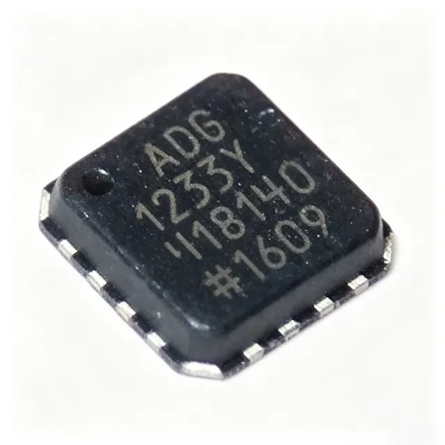
ADG1233YCPZ-REEL7 - Triple SPDT Analog Switch | Analog Devices
The ADG1233YCPZ-REEL7 is a monolithic iCMOS® analog switch from Analog Devices, integrating three independently selectable single-pole, double-throw (SPDT) switches in a compact 16-lead LFCSP-VQ (4x4 mm) package. It operates over a wide supply range of ±15 V or +12 V, with a low on-resistance of 120 Ω (typical) and ultra-low capacitance of 1.5 pF off capacitance, making it ideal for high-performance signal routing in precision instrumentation, audio, and data acquisition systems. An analog switch is a semiconductor device that selectively connects or disconnects an analog signal path under digital control. It is a fundamental building block in signal routing, multiplexing, and sample-and-hold circuits. The ADG1233 belongs to the family of analog switches and multiplexers, which are part of the broader category of interface ICs and signal conditioning components. Its iCMOS® (industrial CMOS) process technology ensures low power consumption and high voltage handling, bridging the gap between traditional CMOS and higher-voltage bipolar processes. Key features include break-before-make switching action, which prevents momentary shorting when switching channels, and an EN input that enables or disables the entire device. The switch is fully specified with 3 V logic-compatible inputs, allowing direct interface with low-voltage digital controllers. Rail-to-rail operation ensures minimal signal distortion across the full supply range. The 1.5 pF off capacitance and 0.5 pC charge injection minimize signal degradation in high-frequency and precision applications. The ADG1233 utilizes a proprietary iCMOS® process that combines the advantages of high-voltage CMOS with low power dissipation. This architecture enables the device to handle ±15 V supplies while maintaining low leakage currents and fast switching speeds. The break-before-make action is implemented through internal timing circuitry, ensuring reliable channel isolation during transitions. The device is available in a 16-lead LFCSP-VQ package, which offers excellent thermal performance and a small footprint for space-constrained designs. Typical applications include audio signal routing, precision data acquisition systems, automatic test equipment (ATE), and medical instrumentation. The low capacitance and charge injection make it particularly suitable for high-speed analog signals, while the wide supply range accommodates both bipolar and single-supply designs. The EN pin provides a convenient means of power-down or signal isolation in multi-channel systems. When designing with the ADG1233, ensure that the digital control signals are within the specified logic thresholds and that the supply voltages are properly decoupled with 0.1 µF capacitors close to the VDD and VSS pins. The break-before-make feature eliminates the need for external timing circuits, but the user should verify that the switching time meets system requirements.

ADG1236YCPZ-500RL7 - Dual SPDT ±15V iCMOS Analog Switch | ADI
The Analog Devices ADG1236YCPZ-500RL7 is a low-capacitance, low-charge-injection dual SPDT (single-pole double-throw) analog switch fabricated on the iCMOS process, offering a 33 V supply range, 1 pC charge injection, and 1.3 pF off capacitance in a 12-lead LFCSP (3 mm x 3 mm) package. An analog switch is an electronic component that routes or blocks analog signal paths under digital control. Within the signal-chain hierarchy, it belongs to the multiplexer/switch family of interface ICs, sitting between sensors or signal sources and amplifiers, ADCs, or measurement front ends. SPDT switches route one common terminal to one of two throw terminals, enabling source selection, gain-range switching, and redundant-path switchover in precision systems. Key features include 1.3 pF off capacitance and 3.5 pF on capacitance, which minimize signal distortion in high-frequency and capacitive-sensitive nodes, and 1 pC charge injection that reduces glitches when switching precision sample-and-hold or integrator circuits. The 33 V supply range supports +/-15 V dual-supply and 12 V single-supply operation, and the iCMOS process combines high-voltage CMOS and bipolar technologies for industrial-grade robustness. Logic inputs are 3 V logic-compatible and no VL supply pin is required, simplifying interfacing with low-voltage controllers. Technically, the iCMOS process allows high-voltage analog handling with low-voltage digital control, so the switch blocks up to +/-15 V signals while the control logic accepts standard 3.3 V or 5 V levels. The monolithic CMOS construction ensures low power and matched switch behavior across both SPDT channels, which switch independently for flexible routing. Typical applications include automated test equipment (ATE) signal routing, data-acquisition channel selection, precision sample-and-hold circuits, and industrial instrumentation where large-swing signals meet low-glitch switching requirements. Design consideration: on resistance is approximately 120 ohm typical (190 ohm maximum per DigiKey listing), so account for Ron flatness and voltage drop in high-impedance or precision-gain paths. This page synthesizes distributor pricing, drop-in alternative analysis, and practical design notes not found in the manufacturer datasheet, with data verified as of 2026-09-10.
ADG1408YRUZ - 8:1 CMOS Analog Multiplexer | Analog Devices
The Analog Devices ADG1408YRUZ is an 8:1 CMOS analog multiplexer with a maximum on-resistance of 4.7 ohms at 25°C, continuous current up to 190 mA, and 3 V-compatible logic inputs in a 16-lead TSSOP package. It switches one of eight inputs to a common output according to three binary address lines, A0, A1, and A2. An analog multiplexer is an analog switch network that connects one selected source channel to a shared destination. In the ADG1408, eight single-ended inputs are multiplexed onto one output. The address inputs control the selected path, while the common output provides a compact way to route signals in test equipment, data-acquisition systems, relay-replacement circuits, and audio/video equipment. This places the device in the interface IC hierarchy: analog switch → multiplexer → signal-routing IC. Key features include a maximum on-resistance of 4.7 ohms, on-resistance flatness of 0.5 ohm, rail-to-rail operation, and break-before-make switching. The manufacturer lists operation across ±15 V, +12 V, and ±5 V supplies, plus compatibility with 3 V logic inputs. These features make the ADG1408 suitable for systems that require controlled switching of bipolar or low-voltage signals while maintaining defined break-before-make behavior. The ADG1408YRUZ is specified in a 16-lead TSSOP package. Its 4.7-ohm maximum on resistance and 190-mA continuous-current capability provide useful performance for precision signal routing, although insertion loss and settling behavior depend on the source impedance, load, signal frequency, supply voltage, and layout. The 0.5-ohm on-resistance flatness helps minimize resistance variation across the selected switch network. Typical applications include relay replacement, audio and video routing, automatic test equipment, data-acquisition systems, and signal-path multiplexing. The break-before-make action is particularly useful where briefly connecting two externally driven sources is undesirable. For high-speed or high-impedance systems, engineers should evaluate switch capacitance, off leakage, charge injection, and clock timing in the complete signal path. The principal design consideration is ensuring that address transitions do not create an undesirable transient at the common output. Use the manufacturer-recommended supply bypassing, keep routing short, and account for the TSSOP footprint and pin orientation. This page combines the verified manufacturer and distributor information with engineering-oriented application guidance and sourcing details.
ADG1408YRUZ-REEL7 - 8:1 iCMOS Mux, 4.7Ω Ron, 16-TSSOP | ADI
The Analog Devices ADG1408YRUZ-REEL7 is a monolithic iCMOS analog multiplexer that switches one of eight inputs to a common output, controlled by a 3-bit binary address (A0, A1, A2), housed in a 16-pin TSSOP (Y) package supplied on a 7-inch reel. It provides a typical on resistance (Ron) of 4.7Ω and a maximum Ron of approximately 5Ω across the specified signal range. An analog multiplexer (mux) is an analog switch array that time-multiplexes multiple analog input signals onto a single output line, allowing a microcontroller or ADC to sequentially sample many channels using only one ADC input. In the broader hierarchy, the ADG1408 belongs to the analog switch family, itself a subset of signal routing and interface ICs. The iCMOS (industrial CMOS) process used by Analog Devices combines high-voltage bipolar, CMOS, and DMOS transistors on a single die, enabling ±15 V / +12 V / ±5 V dual-supply operation while keeping leakage and Ron low. Key differentiating specifications include a 4.7Ω typical on-resistance, ±15 V dual-supply tolerance, low power consumption, latch-up proof construction, and break-before-make switching that prevents momentary shorting of input channels during channel transitions. The 3-bit binary address logic allows a simple GPIO or decoder to drive selection. The iCMOS architecture delivers high voltage tolerance with low Ron and low charge injection, making the ADG1408 suitable for industrial process control, instrumentation, and audio routing. Unlike low-voltage CMOS muxes (e.g., 4051-family parts limited to ~5 V), the iCMOS process lets designers route ±10 V or ±15 V signals directly without external level shifting. Typical applications include industrial process control PLCs, multi-channel data acquisition (DAQ) front-ends, audio/video signal routing, ATE (automatic test equipment) pin switching, and medical monitoring multiplexers. It is commonly paired with 16/18-bit ADCs to expand channel count. A key design consideration is supply sequencing: while iCMOS parts tolerate standard supplies, designers should add 100 nF decoupling close to VDD/VSS and consider ESD protection on field-side inputs. Break-before-make behavior eliminates cross-couples but limits simultaneous-channel sampling, so for simultaneous sampling use a per-channel amplifier + SAR front-end instead. This page synthesizes distributor pricing, drop-in alternatives in the same 16-TSSOP footprint, and practical design notes not found in the manufacturer datasheet alone.

ADG1411YCPZ-REEL7 - Quad SPST 1.8Ω Switch iCMOS | ADI
The Analog Devices ADG1411YCPZ-REEL7 is a monolithic CMOS device containing four independently selectable single-pole single-throw (SPST) switches fabricated on ADI's iCMOS (industrial CMOS) process. The device features 1.8 Ω typical on-resistance, ±4.5 V to ±16.5 V dual-supply operation (or up to 12 V single-supply), 1.5 Ω on-resistance flatness, and is housed in a 16-lead LFCSP-VQ (4x4 mm) package. The four switches are normally-open (NO) types, sharing a common logic supply pin that interfaces directly to TTL and CMOS logic levels. An analog switch IC is a solid-state semiconductor device that uses MOSFET transistors to route analog signals between input and output terminals under digital control. SPST (single-pole single-throw) switches form the foundational building block of signal routing hierarchies: SPST -> SPDT -> multiplexer -> switch matrix -> signal chain. Analog switches sit at the boundary between the analog signal domain (where high linearity, low distortion, and low leakage are required) and the digital control domain (where logic-level compatibility is mandatory), making them essential in test equipment, instrumentation, data acquisition, and communication systems. Key specifications include a 1.8 Ω on-resistance (RON), 0.5 Ω channel-to-channel matching, 5 pC charge injection per switch transition, a -3 dB bandwidth of 115 MHz, and a turn-off isolation/break-before-make timing of 30 ns typical. The device operates from -40 °C to +125 °C extended industrial temperature range, drawing a quiescent supply current of typically 1 nA. The LFCSP-VQ-16 package integrates an exposed thermal pad that drops the junction-to-ambient thermal resistance to 33 °C/W on a standard JEDEC 4-layer board. The iCMOS architecture combines high-voltage CMOS transistors with submicron lateral bipolar structures on the same die, enabling analog signals up to ±16.5 V in a footprint that would otherwise require a larger 28 V bipolar process. This allows the ADG1411 to directly handle industrial-level signals without external level shifting, while still presenting logic inputs that are 1.8 V CMOS- and TTL-compatible. The break-before-make switching architecture prevents momentary shorting of signal sources during transitions. Typical applications include automated test equipment (ATE) pin electronics, precision data acquisition front-ends, audio/video signal routing, medical instrumentation multiplexing, industrial process control input switching, communication system gain-stage switching, and battery-powered portable instrumentation where the nanoampere quiescent current extends battery life. When designing with this part, place the exposed pad (pin 0) on a continuous copper ground plane with at least 16 thermal vias for heat extraction; bypass both VDD and VSS with 0.1 μF ceramic capacitors placed within 50 mm of the supply leads to control digital switching transients. Unused logic inputs must be tied to GND or VDD - never left floating - to prevent spurious channel activation. This page synthesizes distributor pricing from DigiKey, Mouser and Arrow, parameter-accurate drop-in alternatives, and practical PCB layout notes not found in the manufacturer datasheet.

ADG1434YRUZ-REEL7 - Quad SPDT 4.7Ω iCMOS Switch | ADI
The Analog Devices ADG1434YRUZ-REEL7 is a monolithic industrial CMOS (iCMOS®) analog switch integrating four independently selectable single-pole, double-throw (SPDT) channels in a 20-pin TSSOP package. Each channel exhibits a maximum 4.7 Ω on-resistance, 0.5 Ω on-resistance flatness, and rail-to-rail signal handling, all specified for ±15 V, +12 V, and ±5 V dual or single-supply operation. The 33 V supply maximum rating provides substantial transient headroom for industrial bus and instrumentation signal chains. An analog switch, sometimes called a CMOS switch or a bilateral switch, is a solid-state device that uses MOSFET transistors to pass or block analog signals with near-zero quiescent current. Analog switches sit hierarchically below multiplexers (MUX), which combine multiple switches with channel-selection logic, and belong to the broader Interface IC family that bridges real-world analog signals and digital control. Within this taxonomy, the ADG1434 specifically occupies the multi-channel SPDT niche — useful for signal routing, gain switching, sample-and-hold multiplexing, and audio/video signal steering where four channels are required. Key features include break-before-make switching action that prevents momentary shorting when channels change state, fully specified 3 V logic-compatible digital inputs for direct microcontroller interface without level shifters, and a TTL/CMOS-compatible enable input (active low) on selected package variants. The part achieves low power consumption suitable for battery-influenced portable systems while tolerating the bipolar supply rails demanded by precision analog front ends. The integrated iCMOS process enables the combination of high voltage tolerance, low on-resistance, and small TSSOP footprint that discrete relay or opto-isolated solutions cannot match. Typical applications include precision data-acquisition front ends, industrial process-control multiplexers, PLC analog input modules, instrumentation signal switching, medical monitoring routing, automated test equipment (ATE) channel selection, and audio/video signal routing in broadcast or studio equipment. The 4.7 Ω typical on-resistance and low charge injection make it suitable for 16-bit and lower-precision systems where signal-fidelity errors from RON contribute minimally to overall measurement uncertainty. When designing with this part, ensure logic inputs are driven with clean CMOS levels and that the analog signal range stays within both supply rails plus a small margin. Use adequate PCB ground copper and bypass the supply pins with 100 nF ceramic capacitors placed close to the package. The TSSOP-20 footprint is shared across the ADG1433 (3-channel), ADG1434 (4-channel), and ADG1436/ADG1439 families, enabling layout reuse across design variants. This page synthesizes distributor pricing, drop-in alternatives, and practical design notes not found in the manufacturer datasheet alone.
ADG1611BCPZ-REEL7 - 1Ω Quad SPST Switch | Analog Devices
The Analog Devices ADG1611BCPZ-REEL7 is a quad single-pole single-throw (SPST) CMOS analog switch with 1 Ω typical on-resistance, housed in a 16-lead LFCSP-VQ (4 mm × 4 mm) package. The part contains four independent SPST switches that turn on with Logic 0 on the appropriate control input, conduct equally well in both directions, and accept input signal ranges that extend to the supplies. The -REEL7 suffix indicates a 7-inch (1500-piece) tape-and-reel packaging option. An analog switch (also called a CMOS switch or analog multiplexer switch) is a solid-state device that uses MOSFET transistors to route analog or digital signals between input and output pins under digital control. The ADG1611 sits within the broader hierarchy: analog switch → multiplexer/switch IC → interface IC → signal conditioning → data acquisition. Compared with electromechanical relays, CMOS analog switches offer vastly faster switching speeds, lower power consumption, no mechanical wear, and much smaller PCB footprint, at the cost of finite on-resistance and a limited signal-bandwidth product. Key features include 1 Ω typical on-resistance, 0.2 Ω on-resistance flatness across the signal range, ±3.3 V to ±8 V dual-supply operation, and 3.3 V to 16 V single-supply operation. The device does not require a V_L logic supply, accepts 3 V logic-compatible inputs directly, and supports rail-to-rail operation. Continuous current per channel is rated at 280 mA in the LFCSP package and 175 mA in the TSSOP variant. The ADG1611 is built on Analog Devices' iCMOS (industrial CMOS) process technology, which combines high-voltage analog capability with sub-µm CMOS digital logic on a single die. Typical applications include precision signal routing in data-acquisition front-ends, video and audio signal switching, ATE (automated test equipment) channel selection, instrumentation gain-stage multiplexing, communications systems, and battery-powered portable designs that benefit from the wide single-supply range. The wide supply tolerance also makes the device suitable for ±5 V industrial analog rails. When designing with the ADG1611, keep in mind that on-resistance varies with the input signal level (typical flatness is 0.2 Ω), so the part is not ideal for applications requiring gain-invariant signal chains without compensation. Add 0.1 µF decoupling capacitors close to VDD and VSS pins, and ensure unused logic inputs are tied to a valid logic level to prevent unwanted channel activation. This page synthesizes verified distributor pricing, drop-in alternative MPNs, parametric comparison tables, and practical design notes not found in the manufacturer datasheet alone.
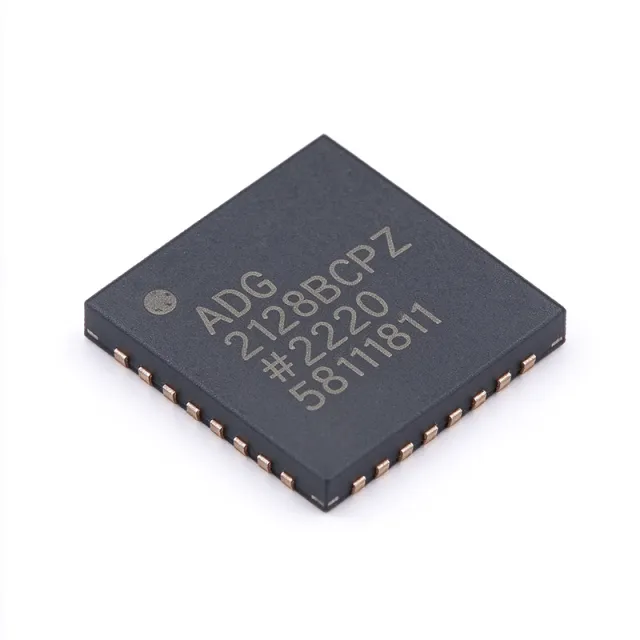
ADG2188BCPZ - 8x8 Analog Crosspoint Switch | Analog Devices
The ADG2188BCPZ is an 8x8 analog crosspoint switch from Analog Devices, designed for routing analog signals in telecommunications, ultrasound, and audio applications. It features 64 bidirectional switch channels arranged in an 8x8 array, with each switch individually addressable via an I2C-compatible interface. The device operates from a single 3.3V or 5V supply and is available in a 32-lead LFCSP-VQ (5x5 mm) package. An analog crosspoint switch is a matrix of switches that connects any input to any output, enabling flexible signal routing without external wiring. It is a key building block in signal routing systems, allowing multiple signals to be directed to different destinations under software control. The ADG2188 belongs to the family of analog switches and multiplexers, which are essential in applications requiring signal distribution and switching. Key features include low on-resistance, low leakage currents, and high bandwidth, ensuring minimal signal distortion. The I2C interface supports standard, full, and fast modes, allowing easy integration with microcontrollers. The device also includes an address pin for multiple device configuration on the same bus, and a reset pin for initialization. Technically, the ADG2188 uses CMOS technology to achieve low power consumption and high switching speed. The switch array is bidirectional, meaning rows and columns can be configured as inputs or outputs, providing flexibility in signal routing. The device also features break-before-make switching to prevent momentary short circuits during channel changes. Typical applications include telecommunications switching, ultrasound imaging, audio routing, and automatic test equipment. In telecommunications, it can route multiple channels in a central office; in ultrasound, it can switch transducer elements; in audio, it can route signals in mixing consoles. When designing with the ADG2188, ensure proper decoupling of the power supply and careful layout to minimize crosstalk. The I2C address pins should be set correctly to avoid bus conflicts. The device is RoHS compliant and suitable for surface-mount assembly.

ADG2188BCPZ-RL7 - 8x8 Analog Crosspoint Switch | Analog Devices
The ADG2188BCPZ-RL7 is an I2C CMOS 8x8 unbuffered analog switch array from Analog Devices, designed for routing analog signals in telecommunications, ultrasound, and audio applications. It provides 64 bidirectional switch channels arranged in eight columns by eight rows, with each switch individually addressable via a standard I2C-compatible interface. The device operates from dual or single supplies, supporting a wide analog signal range, and is housed in a compact 32-lead LFCSP-VQ (5x5 mm) package. An analog crosspoint switch is a type of analog switch array that allows any input to be connected to any output, enabling flexible signal routing without mechanical relays. It is a key building block in signal routing and switching systems, sitting between discrete analog switches and full digital crosspoint ICs in the signal chain hierarchy. The ADG2188's 8x8 matrix provides a balance of channel count and package size, making it suitable for dense PCB designs. Key features include a low on-resistance of [DATA_NEEDED: on-resistance] ohms, low leakage currents, and a wide operating voltage range. The I2C interface supports standard and full-speed modes, allowing easy integration with microcontrollers. The device also features a reset pin and address pins for multiple device configuration on the same bus. Its bidirectional architecture simplifies PCB layout by allowing rows and columns to be configured as inputs or outputs. Technically, the ADG2188 uses CMOS technology to achieve low power consumption and high signal integrity. The unbuffered architecture preserves signal fidelity, making it ideal for precision analog applications. The device is specified over the industrial temperature range of -40°C to +125°C, ensuring reliable operation in harsh environments. Typical applications include telecommunications switching, ultrasound imaging systems, audio routing, and automated test equipment. In ultrasound, the ADG2188 routes transducer signals to processing channels, while in audio, it enables flexible mixing and routing. Its low distortion and high bandwidth make it suitable for high-frequency signals. When designing with the ADG2188, ensure proper decoupling on the supply pins and consider the on-resistance flatness for precision applications. The I2C address pins allow up to [DATA_NEEDED: number of addressable devices] devices on a single bus, enabling large switch matrices.