Interface ICs
Subcategories
Products (3,400+)

SK8120GNY - Interface Specialized IC | onsemi | Audio/Video Link
The onsemi SK8120GNY is an interface specialized integrated circuit originally designed by Fairchild Semiconductor (now part of onsemi) for analog video signal routing in consumer and industrial electronics. Housed in a compact surface-mount package, the device integrates multiple switching functions optimized for low-noise signal paths where common ground structures are used throughout the design. An interface specialized IC (also called a video/audio interface controller) is a category of mixed-signal semiconductor that bridges analog signal sources and downstream processing blocks. These parts sit at a clear hierarchical level: interface specialized -> interface IC -> signal chain IC -> mixed-signal semiconductor. They typically include internal multiplexers, gain stages, and sometimes clamp circuits that comply with broadcast standards. Engineers select these parts when a system requires conditioned routing of composite or component video, audio, or other analog baseband signals without the cost and complexity of a fully programmable serializer/deserializer. Key characteristics include wide operating supply compatibility, low on-resistance signal paths, and integrated ESD protection on the analog I/O lines. The SK8120GNY is engineered for applications that demand compact board area, robust ESD survival on frequently-handled ports, and stable DC biasing of internal switching nodes. Because the original datasheet predates public web archival by several years, exact parametric figures (on-resistance, bandwidth, ESD rating) should be obtained from the manufacturer before committing to a PCB layout. Typical deployment scenarios include analog video switches in set-top boxes, audio/visual input selectors on legacy AV receivers, multi-source switchers in industrial inspection equipment, and signal routing blocks inside instrumentation front-ends. The GNY suffix indicates the specific onsemi/Fairchild package and reel orientation code, and it is electrically and pin-identical to the base SK8120 die. When designing with this part, confirm the input common-mode range against the upstream coupling network and observe the recommended decoupling scheme (typically a 0.1 µF ceramic in parallel with a 10 µF bulk cap near the supply pin). Layout should keep analog traces short and shielded by a continuous ground pour to preserve noise immunity. This page synthesizes distributor pricing, drop-in alternatives, and design notes not found in the original manufacturer datasheet.
SM2258 - SATA 6Gb/s TLC SSD Controller | Silicon Motion
Silicon Motion Technology Corp. SM2258 is a SATA 6Gb/s solid-state drive controller with NANDXtend error-correcting code technology, designed for client SSDs using 3D triple-level cell NAND. The controller targets HDD replacement, ultrabook, and tablet storage systems and provides a complete merchant ASIC and firmware solution. It uses four NAND channels, supports external DDR3 cache, and includes SLC caching and Direct-to-TLC algorithms to improve burst and sustained write performance. A SATA solid-state drive controller is the interface between a host using the Serial ATA protocol and NAND flash memory. Unlike a conventional HDD controller, an SSD controller manages flash translation, wear leveling, error correction, garbage collection, mapping, and the differences between NAND pages and blocks. In the product hierarchy, SM2258 is a storage controller, SSD controller, interface controller, and semiconductor. The verified source identifies SM2258 as a high-performance SATA 6Gb/s controller for client SSDs. Its NANDXtend technology is intended to provide comprehensive data protection and improve the endurance and retention of 3D TLC NAND. The controller is described as delivering more than three times the performance of conventional solutions for 3D TLC SSDs, although the supplied excerpt does not provide a standardized test condition for that claim. The controller supports 3D TLC NAND from major NAND suppliers and uses four channels for parallel flash access. External DDR3 cache can improve host-interface responsiveness and sustained operation. SLC caching accelerates burst workloads by temporarily writing data to SLC regions, while Direct-to-TLC algorithms are intended to reduce the performance penalty associated with writing directly to lower-endurance TLC NAND. Typical applications include 2.5-inch SATA SSDs, M.2 2280 SATA SSDs, ultrabook storage, tablet storage, and HDD-replacement client drives. The Viking Technology application documents specifically show SM2258-based 2.5-inch and M.2 2280 SATA SSD designs, including external DDR3 cache and SLC caching. Design integration requires careful validation of the selected NAND, DDR3 devices, firmware, power rails, signal integrity, and SSD qualification. NAND compatibility is not determined solely by the controller name; flash identifiers, timing, channel organization, firmware support, and target SSD workload must all be confirmed with the manufacturer or SSD vendor. The supplied sources do not establish a public pinout, package dimensions, pricing, or lead time, so those values are intentionally not inferred.

SM2259XT2 - DRAM-less 2-Ch SATA 6Gb/s SSD Controller | SMI
The Silicon Motion SM2259XT2 is a DRAM-less, 2-channel, high-performance SATA 6Gb/s SSD controller in a TFBGA-144 (8x8 mm) package, designed for cost-effective, small-form-factor client SSDs. It is the 2-channel successor in the SM2259 family and supports SATA revision 3.1 (6 Gb/s) host interface with backward compatibility to SATA 3 Gb/s and SATA 1.5 Gb/s. Unlike DRAM-based controllers, the SM2259XT2 eliminates external DRAM to reduce BOM cost while still delivering mainstream client SSD throughput, making it well-suited for mainstream M.2, mSATA, slim SATA (MO-297), and 2.5" SSDs targeting notebooks, desktops, and entry client compute. An SSD controller (Solid-State Drive controller) is the central ASIC inside an SSD that bridges the host interface (SATA or PCIe) to the NAND flash media. It runs the Flash Translation Layer (FTL), performs wear leveling, garbage collection, bad-block management, and applies ECC to maintain data integrity across the NAND array. The SM2259XT2 is a DRAM-less variant, meaning it uses a portion of the host system's memory or on-chip SRAM for FTL mapping instead of an external DRAM cache, which reduces BOM cost and PCB footprint in space-constrained designs. The SATA host interface positions SM2259XT2 in the mainstream client SSD market, where cost and low power are dominant priorities over the highest throughput. Key features include support for Toggle 2.0/3.0 and ONFI 3.0/3.1/3.2 NAND interface, integrated NANDXtend ECC with LDPC hard-decision and soft-decision decoding for improved endurance and retention, and 2 channels with up to 4 CE (Chip Enable) targets per channel for flexible NAND array sizing. The controller supports 2D MLC, 3D TLC, and 3D QLC NAND from major flash vendors, enabling a wide range of capacity and cost targets. It operates at ultra-low power to extend mobile battery life, and integrates hardware AES-128/256 for OPAL-based self-encrypting drive (SED) functionality. The SM2259XT2 uses an SMI-developed 32-bit embedded CPU core with hardware accelerators for NAND interface and ECC. The 2-channel architecture (vs 4-channel on SM2259) is the key differentiator from its predecessor: by halving the channel count and integrating DRAM-less operation, the XT2 targets cost-sensitive client SSDs where sequential throughput above ~560 MB/s is not required. The integrated LDPC ECC engine corrects bit errors across MLC/TLC/QLC endurance transitions and supports RAID-like parity across channels for data path reliability. Typical applications include 2.5" SATA SSDs for desktops and notebooks, M.2 2280/2242 client SSDs, mSATA and slim SATA (MO-297) modules, retail SSD upgrade kits, and external USB-SATA enclosures. Its small BGA footprint and low power also make it attractive for industrial embedded storage and boot drives. Compared with DRAM-based controllers, the SM2259XT2 trades peak random 4K IOPS for lower cost, while retaining mainstream sequential throughput. When designing with the SM2259XT2, allocate PCB real estate for proper power-rail decoupling near the BGA balls and provide adequate thermal copper under the exposed die. Validate the firmware MP tool and flash parameter table against the exact NAND vendor and die stepping before mass production, because mixing SM2259XT2 firmware with SM2258XT or SM2259XT firmware images is not supported. This page aggregates distributor pricing, package drawings, drop-in same-package alternatives, and design notes curated from the manufacturer datasheet, providing engineering context not found in the SM2259XT2 datasheet PDF alone.
SM2261XT - PCIe Gen3 x2 DRAM-less NVMe SSD Controller
Silicon Motion SM2261XT is a DRAM-less NVMe SSD controller with PCIe Gen3 x2 host connectivity, two NAND flash channels, and support for 3D TLC and QLC NAND. The controller operates from a 3.3 V supply, supports NVMe 1.3, and is designed for compact consumer SSD designs, including M.2 and small BGA SSD formats. Its HMB architecture uses host memory caching to reduce system BOM cost while retaining SSD functionality. A PCIe SSD controller is the central conversion and management device between a host computer and nonvolatile flash memory. It handles PCIe transactions, NAND interface activity, flash translation, data protection, wear management, and the mapping between logical blocks and physical NAND pages. The SM2261XT is therefore positioned between a PCIe host interface and 3D NAND storage rather than as a general-purpose processor or memory device. The SM2261XT supports two PCIe Gen3 lanes operating at 8 GT/s per lane and two NAND channels capable of 1,200 MT/s per channel according to the manufacturer product brief. It uses proprietary NANDXtend ECC technology, SRAM ECC, and end-to-end data-path protection to improve NAND error handling, endurance, and retention. Its DRAM-less design reduces external memory requirements and is intended for cost-sensitive, compact consumer storage applications. Typical SSD designs use the controller with 3D TLC or QLC NAND, power-management circuitry, flash channels, thermal management, and an M.2 or BGA package implementation. A listed MTC-C610 Series SSD uses SM2261XT-based configurations from 64GB to 1TB and supports up to 1,700 MB/s read and 1,200 MB/s write under specified flash configurations. These figures describe a finished SSD system, not guaranteed controller-only performance. Designers should verify the exact package, pinout, NAND compatibility, firmware configuration, power rails, thermal limits, and SSD qualification requirements with the manufacturer documentation. The controller supports a 3.3 V operating voltage and NVMe 1.3 according to the provided source material. PCIe Gen3 x2 bandwidth and NAND channel performance must also be evaluated with the selected NAND devices and the complete SSD firmware profile. This product data consolidates manufacturer controller information, SSD application examples, source links, and design cautions for engineers evaluating the SM2261XT. It is not a substitute for the complete manufacturer datasheet, NAND compatibility list, firmware documentation, or SSD validation report.
SM2263XT - PCIe Gen3 x4 NVMe 1.3 SSD Controller | Silicon Motion
The Silicon Motion SM2263XT is a high-performance DRAMless PCIe Gen3 x4 NVMe 1.3 SSD controller targeted at mainstream client and OEM solid-state drives. It delivers four lanes of simultaneous 8 Gbps data flow across a PCIe 3.1 interface and exposes four NAND channels, enabling high sequential throughput without an external DRAM cache thanks to its Host Memory Buffer (HMB) feature set. Per the Silicon Motion product brief, the SM2263XT is optimized for cost-sensitive M.2 NVMe SSDs in client computing. A NAND flash controller is a dedicated processor that manages read, write, erase, wear-leveling, garbage-collection, and ECC operations on non-volatile flash memory behind a high-speed host interface. Within the storage hierarchy the SM2263XT sits between the host PCIe root complex and the raw NAND packages; its family lineage is PCIe Gen3 x4 NAND controller -> NVMe SSD controller -> SSD SoC -> semiconductor IC. Key features include PCIe Gen3 x4 (four 8 Gbps lanes), NVMe 1.3c compliance, four NAND channels, HMB support for DRAMless operation, LDPC ECC with hardware RAID, end-to-end data path protection, and AES-256 hardware encryption. The controller is paired typically with 64-layer 3D TLC or QLC NAND and supports 2D MLC/TLC, 3D MLC/TLC/QLC, and SLC-cache architectures used in mainstream SSDs such as the HP EX900, Mushkin Helix-L, Patriot P300, Lexar NM610 Pro, and Transcend 110S. Architecturally the SM2263XT shares its firmware base and silicon platform with the SM2263EN, differing mainly in DRAMless vs. DRAM-equipped variants. The controller offloads the host-side DRAM footprint to the system memory via NVMe HMB, allowing 256 GB to 1 TB single-sided M.2 2280 SSDs to ship at lower BOM cost while still achieving sequential reads up to roughly 2400 MB/s in shipped OEM drives. Typical applications include mainstream client NVMe SSDs, OEM pre-installed boot drives, M.2 2280 retail SSDs, Ultrabook upgrades, and DRAMless entry-level NVMe storage. The HMB dependency means the SM2263XT requires NVMe HMB-capable host operating systems (Windows 10 / modern Linux kernels) for full performance. When designing an SSD around the SM2263XT, allocate sufficient PCIe lane routing on the M.2 edge connector and validate NVMe HMB support across target operating systems, since host memory must be reserved for the controller's translation table. The SM2263XT is shipped to SSD OEMs only and is not sold through catalog distributors; consumer SSDs based on this controller are widely available retail instead. This page synthesizes manufacturer brief specifications, drop-in related controllers, application notes, and design guidance not duplicated on any single distributor page.
SM2264 - PCIe Gen4 x4 NVMe SSD Controller | Silicon Motion
The Silicon Motion SM2264 is a merchant PCIe Gen4 x4 NVMe 1.4 SSD controller ASIC with four PCIe lanes operating at 16 Gb/s per lane and a quad-core ARM R8 CPU. It is packaged for next-generation SSD designs ranging from mainstream client drives to small-form-factor and automotive SSDs, and its package details are provided as [DATA_NEEDED: package designation]. The controller supports 3D NAND from major suppliers and uses Silicon Motion NANDXtend ECC technology to improve NAND endurance, data retention, and data integrity. A PCIe NVMe SSD controller is the semiconductor platform that coordinates the host PCIe interface, NAND interface, firmware, error correction, and storage-management functions in a solid-state drive. In the hierarchy of semiconductor devices, the SM2264 is an interface and storage-controller IC rather than a memory package or a complete SSD. Its Gen4 x4 interface provides a high-bandwidth path between a host computer and the NAND storage subsystem. Key verified features include four PCIe lanes at 16 Gb/s, NVMe 1.4 support, eight NAND channels, quad-core ARM R8 processing, NANDXtend ECC, SRAM ECC, and end-to-end data-path protection. The controller is intended for SSDs rather than general-purpose computing, and its performance depends on the selected NAND packages, firmware, DRAM configuration, thermal design, and the complete SSD implementation. Exact core frequency, power ratings, operating temperature, package dimensions, and NAND-interface data rate were not included in the provided data and are marked for validation. The SM2264 is suitable for client NVMe SSDs, compact M.2 drives, high-performance gaming storage, industrial storage platforms, and automotive SSD designs when the system requirements match the controller and its qualified firmware. Automotive implementations may require the automotive-qualified SM2264XT-AT variant and full product qualification rather than the standard SM2264 designation. Designers should validate the complete reference design, PCB stack-up, power rails, NAND compatibility, firmware release, thermal solution, and end-to-end data-integrity requirements before production. PCIe Gen4 x4 link integrity, power delivery, NAND routing, and thermal margin are critical because controller features alone do not determine final SSD performance. This page synthesizes the verified manufacturer and industry-source material, while unavailable electrical, package, pinout, pricing, and lifecycle details remain explicitly unconfirmed.

SN65173D - Quad Differential Line Receiver | Texas Instruments
Texas Instruments SN65173D is a monolithic quadruple differential line receiver with 3-state outputs, packaged in a 16-pin small-outline integrated-circuit package. It accepts four differential signal pairs and supports balanced digital-data transmission interfaces covered by TI A/EIA-422-B, TIA/EIA-423-B, TIA/EIA-485-A, and related ITU recommendations. The receiver's -40°C to +85°C temperature range suits industrial equipment, instrumentation, industrial automation, and communications systems. The SN65173D is the taped-and-reel ordering option identified for the D package in the SN55173, SN65173, and SN75173 device family. A differential line receiver is an interface IC that compares two complementary signal lines and converts their voltage difference into a logic-level output. In the broader semiconductor hierarchy, the SN65173D belongs to the receiver category, then to line-driver and transceiver interface ICs, and ultimately to interface semiconductors. Differential signaling rejects common-mode noise, reduces sensitivity to ground offsets, and supports reliable data transfer over cables or backplanes. A quadruple receiver consolidates four channels into one package, reducing board area when several links share a communications subsystem. The principal feature of the SN65173D is its four-channel differential input arrangement with 3-state outputs. The 3-state output capability permits the receiver outputs to be placed into a high-impedance state when the shared bus is disabled, allowing multiple devices to share a data path under suitable bus-management conditions. Its monolithic construction provides four receivers on one die, while the compact 16-pin package supports conventional surface-mount assembly. The manufacturer identifies the D package as available in taped-and-reel form. The SN65173 family is designed for balanced multipoint data transmission where common-mode rejection is important. Its applications include industrial control networks, data-processing equipment, test systems, and interfaces using differential signaling. Compatibility with the listed EIA/TIA and ITU recommendations provides an established framework for signal voltage, loading, and bus behavior. Exact input thresholds, common-mode range, propagation delay, output timing, enable logic, and supply-current limits should be confirmed in the manufacturer datasheet before final circuit sign-off. Typical uses include industrial serial links, data-acquisition equipment, instrumentation interfaces, and embedded control systems. In a multi-drop bus, the receiver can monitor a differential pair at a remote device while retaining a tri-state output for controlled bus participation. Designers should confirm that all attached transmitters, receivers, terminations, and grounding arrangements satisfy the applicable standard, particularly on long cables or electrically noisy factory environments. A principal design consideration is the distinction between receiver enable and bus-driver enable. The SN65173D is a receiver only, so it requires a separate line driver when the design must transmit on the same physical bus. Its differential inputs and single-ended logic outputs also require an intentional grounding and signal-integrity strategy. Use the datasheet pin-description and typical-application diagrams when assigning traces and logic functions, and check timing margins across the complete transmitter-to-receiver path. This page consolidates the verified package, temperature, receiver-function, family-option, and application information into a design-oriented reference. It also identifies the closest package-compatible alternatives, highlights the distinction between receiver-only and transceiver solutions, and provides comparison and implementation guidance that helps engineers select the correct device before PCB layout.

SN65C1168PW - Dual RS-422/RS-485 Driver/Receiver | Texas Instruments
The Texas Instruments SN65C1168PW is a dual differential driver and receiver pair designed for balanced transmission lines, packaged in a 16-pin TSSOP (PW) and compliant with TIA/EIA-422-B and ITU-T V.11. It integrates two drivers and two receivers operating from a single 5 V supply, with each driver featuring its own active-high enable input for independent direction control in half- or full-duplex RS-422/RS-485 links. A line transceiver is an interface IC that converts digital logic-level signals (typically CMOS/TTL) into the balanced differential voltages required by RS-422 and RS-485 physical layers. RS-422 (TIA/EIA-422-B) supports multi-point (one driver, up to 10 receivers) signaling with a signaling rate up to 10 Mbps and ±7 V common-mode range on the bus; RS-485 (TIA/EIA-485-A) extends this to true multi-drop (32 drivers/receivers on a bus) with similar rate and noise immunity. The SN65C1168 belongs to the broader hierarchy of UART-to-bus transceivers within the wired-interface family, and it is commonly specified for industrial-control, instrumentation, and point-of-sale backplanes where robust differential signaling is required. Key features of the SN65C1168PW include a 5 V single-supply operation, ±25 V bus-pin ESD protection (HBM), 3-state driver outputs, and individual active-high driver enables that allow external tie-off for direction control. The driver delivers differential output voltage meeting RS-422 levels (≥2 V across a 50 ohm load) and supports a signaling rate of up to 10 Mbps, which is sufficient for many Profibus, DMX512, and high-speed industrial-fieldbus links. The receiver presents a 12 kohm typical input impedance and includes a typical 200 mV hysteresis (per datasheet typical characteristics) to reject bus noise in long-cable runs. The architecture pairs a TTL/CMOS-compatible driver input stage with a differential line driver and an RS-422 differential receiver with internal fail-safe biasing, enabling the IC to detect idle bus states without external pull-up/down resistors. The 16-pin TSSOP (PW) package offers a compact 5 mm × 4.4 mm footprint suitable for high-density backplane layouts, and the pinout follows industry-standard dual-driver/receiver conventions so it can often replace the SN75C1168PW (commercial-temperature equivalent), the SN65C1167PW (combined-driver shared-enable variant), or pin-compatible parts from other vendors. Typical applications for the SN65C1168PW include RS-422 point-to-point links in industrial PLC backplanes, multi-drop RS-485 sensor networks, DMX512 stage-lighting links, and any 5 V system that needs one differential driver and one differential receiver per channel with independent high-speed direction control. When designing with this part, the designer should add a 100 nF decoupling capacitor as close as possible to the VCC pin and ensure the bus is terminated at the cable ends with a 120 ohm differential resistor matched to the cable characteristic impedance (typically 120 ohm for RS-485 twisted pair) to suppress reflections. The driver outputs slew at a rate controlled by internal design; for EMI-sensitive designs, consider the slower-slew SN65HVD series for 250 kbps links or the SN65HVD75 for 2 Mbps links with similar pin counts. This page consolidates official TI datasheet information with cross-reference drop-in alternatives, application guidance, and design considerations distilled from typical industrial-bus design practice—information not found on the manufacturer datasheet alone.

SN65DP159RGZT - 6-Gbps HDMI 2.0 Retimer | Texas Instruments
The Texas Instruments SN65DP159RGZT is a 6-Gbps AC-coupled TMDS-to-HDMI level-shifter retimer IC in a 48-pin VQFN (RGZ 7x7 mm) package. It bridges DisplayPort dual-mode (DP++ 1.1) outputs to HDMI 2.0b sinks at data rates up to 6 Gbps per lane, with operating temperature rated from -40C to +85C. The retimer restores signal integrity across lossy cables and bandwidth-limited PCB traces. What is an HDMI retimer? An HDMI retimer (also called a signal conditioner or redriver-with-clock) is a mixed-signal interface IC that receives a degraded TMDS (Transition-Minimized Differential Signaling) stream, recovers its embedded clock, applies equalization and de-emphasis, and re-transmits a clean TMDS signal. Retimers sit in the signal chain hierarchy between TMDS redrivers (which only compensate channel loss) and full HDMI2.1 protocol converters (FRL). Compared with simple redrivers, retimers reduce both ISI jitter and random jitter, enabling HDMI 2.0b 4K60 8-bit signaling over longer cable runs. Key features include adaptive and fixed receiver equalization for ISI compensation, output swing/pre-emphasis/transition-density drive control, integrated I2C control with pass-through EDID/HDCP/HPD logic, and DisplayPort dual-mode 1.1 cable adapter support. The retimer operates from a single 3.3V supply and exposes configurable registers via I2C for sink-side tuning of the recovered link. Architecturally, the SNx5DP159 combines a CTLE (continuous-time linear equalizer) input stage, a CDR (clock-and-data recovery) PLL, and a TMDS driver with programmable pre-emphasis. The 48-pin RGZ package exposes all four TMDS lanes, the auxiliary/HEAC+/DDC pair, and full I2C-side configuration I/O. A smaller 40-pin RSB (WQFN) package version is also offered for space-constrained dongles. Typical applications include HDMI 2.0b dongles and adapters, set-top boxes, notebook and docking stations, 4K TVs and projectors, gaming consoles, and DP++ to HDMI adapters. The chip is also used in HDMI splitter/selector boards that need to clean up jittery inputs from long upstream cables. When designing with this device, place AC-coupling capacitors close to the TMDS input pins as required by HDMI, provide a clean 3.3V rail, and route the I2C lines with pull-ups. The HPD, DDC, and CEC paths must be level-shifted correctly when bridging between 3.3V and 5V HDMI logic. This page synthesizes distributor pricing, drop-in package alternatives, and practical design notes for the SN65DP159RGZT HDMI retimer that are not consolidated on any single manufacturer or distributor page.

SN65DSI83ZXHR - 4 Gbps MIPI DSI to LVDS Bridge | TI
The Texas Instruments SN65DSI83ZXHR is a single-channel MIPI DSI-to-single-link LVDS bridge integrated circuit with a 1 Gbps-per-lane receiver, four data lanes, maximum input bandwidth of 4 Gbps, and a 64-pin NFBGA package measuring 5 x 5 mm. It converts supported MIPI DSI RGB666 and RGB888 packets into FlatLink-compatible LVDS video data while providing low-swing outputs and MIPI ultra-low-power-state support. A display interface bridge belongs to the interface-IC hierarchy and translates physical-layer signaling between a host and a display. In this case, the SN65DSI83 accepts MIPI D-PHY data, formats supported RGB packets, and serializes video onto a single-link LVDS output. This bridge function is useful when a processor or application processor uses DSI internally but the target panel uses FlatLink-compatible LVDS. Verified device features include one DSI channel, four lanes per channel, 1 Gbps operation per lane, and 4 Gbps maximum aggregate input bandwidth. The bridge supports 18 bpp RGB666 and 24 bpp RGB888 packets. Its low-swing LVDS outputs are intended to reduce signal amplitude and electromagnetic-interference concerns, while ULPS support helps the DSI receiver enter the MIPI-defined low-power state. The SN65DSI83ZXHR is identified as a specialized notebook computer interface IC and uses TI's 64-ball nFBGA package designation. The verified distributor listing describes the package as 64-NFBGA, 5 x 5 mm. This dense surface-mount package requires careful PCB escape routing, clean supply distribution, and package-specific land-pattern compliance rather than generic BGA layout assumptions. Typical uses include notebook and embedded display systems, portable computing panels, small-form-factor instruments, and other products that pair a DSI-capable host processor with a FlatLink LVDS panel. Host compatibility remains application-specific because panel timing, resolution, lane configuration, initialization sequence, and connector implementation must all be checked. The most important design step is to follow the manufacturer datasheet for power sequencing, bypass capacitors, D-PHY routing, LVDS output topology, package-ball assignments, and PCB constraints. Do not infer the complete 64-ball pinout from the distributor package name alone; verify each signal and exposed function against the official datasheet before layout release. This page consolidates the verified manufacturer and distributor facts, distinguishes a documented footprint-compatible legacy transition from unverified functional substitutes, and adds selection and layout guidance that are not available as a concise comparison on a distributor listing.

SN65HVD05D - High-Output RS-485 Transceiver | Texas Instruments
The Texas Instruments SN65HVD05D is a high-output, half-duplex RS-485/RS-422 transceiver combining a differential line driver, differential line receiver, and 3-state driver output in an 8-pin SOIC package. It operates from a 4.5 V to 5.5 V supply, provides a minimum differential output voltage of 2.5 V into a 54-ohm load, and is designed for balanced industrial data transmission. An RS-485 transceiver is an interface IC that converts logic-level digital signals into balanced differential signals for reliable communication over longer, potentially noisy cable runs. The SN65HVD05 family supports ANSI TIA/EIA-485-A and ISO 8482E-compliant devices. Its differential signaling and common-mode rejection help maintain data integrity in industrial environments, while the integrated receiver returns the bus state to the host logic. The most notable features include high output drive, 3-state operation, a low 1/8-unit-load option supporting as many as 256 nodes, open-circuit, short-circuit, and idle-bus failsafe receiver behavior, and bus-pin ESD protection exceeding 16 kV HBM. The driver also provides controlled output slew rate to limit electromagnetic interference and reduce ringing on properly terminated networks. The SN65HVD05D combines one driver and one receiver, allowing half-duplex communication when the driver and receiver share the same bus pair. Its differential output is stronger than the minimum commonly required for RS-485 networks, making it useful where bus loading, cable loss, or stub length can reduce signal amplitude. The receiver provides a failsafe response when the bus is disconnected, shorted, or idle. Typical applications include industrial process-control networks, factory automation equipment, building-control systems, instrumentation links, motor-control equipment, and other multidrop RS-485 networks. These systems benefit from balanced differential signaling, while system-level grounding, surge protection, and cable termination remain essential for reliable operation in electrically noisy environments. When designing the circuit, use a low-ESR supply capacitor near the device, connect the bus interface to protected circuitry, and verify that transceiver direction control prevents driver contention. The 54-ohm minimum differential output test condition is not a recommendation to terminate the bus at the transmitter; instead, place the standard termination at the appropriate physical ends of the network. This product page combines verified manufacturer and distributor information, a same-family drop-in comparison, application guidance, and design notes that help engineers evaluate the SN65HVD05D beyond the basic distributor parameter table.

SN65HVD05P - High-Output RS-485 Transceiver | Texas Instruments
Texas Instruments SN65HVD05P is a high-output RS-485 transceiver combining a 3-state differential line driver and differential line receiver, operating from a 4.5 V to 5.5 V supply in an 8-pin PDIP (P) package. It supports the 1/8th unit-load option, allowing up to 256 nodes on a bus, while providing bus-pin ESD protection exceeding 16 kV HBM. An RS-485 transceiver is an interface IC that converts logic-level signals into balanced differential signals for reliable communication over multipoint wired networks. It belongs to the interface transceiver hierarchy: RS-485 transceiver, differential line transceiver, communication interface IC, and semiconductor. The differential signal and selectable driver enable help the SN65HVD05P interoperate with ANSI TIA/EIA-485-A and ISO 8482E compliant devices. Key features include a high-output driver, 3-state driver operation, differential receiver, and driver output slew-rate control. The 1/8th unit-load option supports as many as 256 nodes, making the device useful for larger industrial networks. Bus-pin ESD protection exceeding 16 kV HBM improves robustness in electrically noisy installations, while open-circuit, short-circuit, and idle-bus failsafe-receiver options help define the receiver state when the bus is undriven or impaired. The device integrates a differential transmitter and receiver in one package, reducing board area compared with separate driver and receiver ICs. Its 4.5 V to 5.5 V operating supply supports conventional 5 V equipment. Because the P package has through-hole leads, it is also appropriate for prototypes, legacy industrial controllers, long-lived equipment, and designs where through-hole assembly or hand rework is preferred over a fine-pitch surface-mount footprint. Typical uses include industrial factory automation, building automation, security systems, instrumentation, and industrial data links. The transceiver can connect a controller to a balanced two-wire bus while providing a differential receiver to the logic side. When the bus is not actively driven, the enabled receiver can provide a defined failsafe output depending on the selected device option. Designers should verify termination, biasing, cable length, node count, and common-mode limits against the manufacturer datasheet before deployment. A 120-ohm termination at each physical end, correct fail-safe bias, controlled grounding, and placement of protection devices near the connector help prevent signal-integrity and ESD-related failures. The SN65HVD05P is not a power device, so an SOA chart is not applicable. This product page combines verified manufacturer and distributor information with application guidance, parameter comparison, drop-in family alternatives, and practical interface-design notes to support faster component evaluation and board-level decision making.
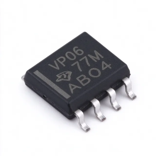
SN65HVD06D - High-Output RS-485 Transceiver, 8-SOIC | Texas Instruments (Tape & Reel)
The Texas Instruments SN65HVD06D is a 3.3V/5V RS-485 half-duplex transceiver in an 8-pin SOIC (D) package, combining a 3-state differential line driver and differential line receiver on a single die. Designed for balanced data transmission, it interoperates with ANSI TIA/EIA-485-A and ISO 8482E compliant devices, and supports data rates up to 10 Mbps in the HVD06 variant. The driver delivers a high differential output voltage greater than the minimum required by these standards, improving noise margin over long cable runs and in harsh industrial environments. An RS-485 transceiver is a bus-interface IC that converts a single-ended TTL/CMOS logic signal into a differential voltage on a twisted-pair cable (typically designated A and B) and, in the opposite direction, converts a received differential signal back into single-ended logic. The differential signaling rejects common-mode noise and allows multi-drop networks of up to 32 (or more with unit-load variants) nodes across cable lengths up to 1200 m. RS-485 transceivers sit at the physical layer of industrial fieldbuses such as Modbus RTU, PROFIBUS, and DMX512, where robust noise immunity is essential. Key features include a minimum 2.5 V differential output voltage into a 54 ohm load (exceeding the 1.5 V TIA/EIA-485-A minimum), 16 kV HBM ESD protection on bus pins, open-circuit, short-circuit, and idle-bus failsafe design, and 1/8th unit-load option that supports up to 256 nodes on the bus. Driver output slew-rate control limits EMI, and the wide 4.5 V to 5.5 V supply range suits both 5 V industrial logic and 3.3 V systems when paired with a charge pump or level shifter. Internally the device uses a differential line driver with controlled slew rate, a window-comparator receiver with input hysteresis, and integrated failsafe biasing that forces a deterministic high output when the bus is idle, shorted, or open. The half-duplex configuration shares one differential pair between transmit and receive, controlled by a single DE/RE logic pin pair, reducing pin count versus full-duplex parts. Typical applications include factory automation networks, motor drive control links, building automation (BACnet, Modbus), solar inverter monitoring, and any industrial point-to-point or multi-drop RS-485 link where high output drive and rugged ESD performance are valued. When designing with this part, always include a 100 ohm termination resistor at each end of the bus and consider fail-safe biasing resistors if the cable can be left floating during commissioning. The high output drive increases quiescent current slightly compared to standard RS-485 parts, so factor thermal dissipation into densely populated multi-channel designs. This document synthesizes distributor pricing, drop-in alternatives, and practical design notes that complement the manufacturer datasheet.
SN65HVD06DR - High-Output RS-485 Transceiver, 8-SOIC | Texas Instruments
The Texas Instruments SN65HVD06DR is a 3.3V/5V RS-485 half-duplex transceiver in an 8-pin SOIC (D) package, combining a 3-state differential line driver and differential line receiver on a single die. Designed for balanced data transmission, it interoperates with ANSI TIA/EIA-485-A and ISO 8482E compliant devices, and supports data rates up to 10 Mbps in the HVD06 variant. The driver delivers a high differential output voltage greater than the minimum required by these standards, improving noise margin over long cable runs and in harsh industrial environments. An RS-485 transceiver is a bus-interface IC that converts a single-ended TTL/CMOS logic signal into a differential voltage on a twisted-pair cable (typically designated A and B) and, in the opposite direction, converts a received differential signal back into single-ended logic. The differential signaling rejects common-mode noise and allows multi-drop networks of up to 32 (or more with unit-load variants) nodes across cable lengths up to 1200 m. RS-485 transceivers sit at the physical layer of industrial fieldbuses such as Modbus RTU, PROFIBUS, and DMX512, where robust noise immunity is essential. Key features include a minimum 2.5 V differential output voltage into a 54 ohm load (exceeding the 1.5 V TIA/EIA-485-A minimum), 16 kV HBM ESD protection on bus pins, open-circuit, short-circuit, and idle-bus failsafe design, and 1/8th unit-load option that supports up to 256 nodes on the bus. Driver output slew-rate control limits EMI, and the wide 4.5 V to 5.5 V supply range suits both 5 V industrial logic and 3.3 V systems when paired with a charge pump or level shifter. Internally the device uses a differential line driver with controlled slew rate, a window-comparator receiver with input hysteresis, and integrated failsafe biasing that forces a deterministic high output when the bus is idle, shorted, or open. The half-duplex configuration shares one differential pair between transmit and receive, controlled by a single DE/RE logic pin pair, reducing pin count versus full-duplex parts. Typical applications include factory automation networks, motor drive control links, building automation (BACnet, Modbus), solar inverter monitoring, and any industrial point-to-point or multi-drop RS-485 link where high output drive and rugged ESD performance are valued. When designing with this part, always include a 100 ohm termination resistor at each end of the bus and consider fail-safe biasing resistors if the cable can be left floating during commissioning. The high output drive increases quiescent current slightly compared to standard RS-485 parts, so factor thermal dissipation into densely populated multi-channel designs. This document synthesizes distributor pricing, drop-in alternatives, and practical design notes that complement the manufacturer datasheet.
SN65HVD06P - 10 Mbps High-Output RS-485 | Texas Instruments
The Texas Instruments SN65HVD06P is a single-channel RS-485/RS-422 interface transceiver providing a differential line driver and differential receiver, a maximum data rate of 10 Mbps, and support for as many as 256 nodes in an 8-pin PDIP package. Its high-output design is intended for balanced data transmission over industrial and commercial RS-485 networks. An RS-485 transceiver is an interface IC that converts logic-level signals into differential bus voltages and reconstructs logic signals from differential bus inputs. It belongs to the interface IC hierarchy and is used where noise immunity, common-mode tolerance, and multi-node bus coordination matter. The SN65HVD06 family interoperates with devices compliant with ANSI TIA/EIA-485-A and ISO 8482E, while the driver produces differential voltage beyond the minimum required by those standards. Key features include a 10 Mbps maximum data rate, a 1/8-unit-load receiver option supporting up to 256 nodes, controlled driver output slew rate, and bus-pin ESD protection exceeding 16 kV HBM. The high-output architecture provides stronger drive capability than standard RS-485 transceivers, making the device useful when longer cables, heavier bus loading, or additional bus margin must be accommodated. The transceiver combines a three-state differential line driver and a differential line receiver. The three-state output allows multiple drivers to share a bus when only one is active at a time, while the receiver supports failsafe operation during open-circuit, short-circuit, and idle-bus conditions. The 1/8-unit-load option lowers the receiver input loading, permitting more nodes than a full-unit-load receiver while preserving balanced signaling. Typical applications include industrial automation, factory equipment, building controls, networked sensors, data acquisition systems, and other balanced multidrop buses. In a multidrop installation, the transceiver can be enabled selectively so that only one driver drives the cable at a time, reducing contention and allowing nodes to be added more densely than on a one-unit-load bus. Designers should provide proper bus termination, maintain common-mode operating limits, and route the differential pair as a controlled impedance network. The 8-pin PDIP package also requires attention to thermal performance and clean supply bypassing. Verify the complete electrical limits, enable logic, and application circuit against the manufacturer datasheet before releasing a production design. This page combines verified distributor pricing, package and interface details, functional alternatives, comparison data, and practical RS-485 design guidance. It also distinguishes documented features from parameters that require confirmation, helping engineers evaluate the SN65HVD06P without treating unverified electrical values as production specifications.
SN65HVD07D - 1 Mbps RS-485 Transceiver | Texas Instruments
The Texas Instruments SN65HVD07D is a 1 Mbps high-output RS-485 half-duplex transceiver with one differential line driver and one differential receiver, packaged in an 8-pin SOIC. It operates from a 4.5 V to 5.5 V supply and combines a three-state differential output stage with a differential input stage. The device is intended for balanced data transmission over multipoint buses and interoperates with ANSI TIA/EIA-485-A and ISO 8482E compliant devices. Its high-output architecture provides a differential output voltage greater than that required by these standards. An RS-485 transceiver is an interface IC that bridges a logic-level controller and a balanced, differential physical bus. The driver converts a single-ended digital signal into differential A and Y outputs, while the receiver converts differential bus voltage into a single-ended logic signal. As a half-duplex transceiver, it supports one physical communication path that can transmit or receive, but not both simultaneously. The SN65HVD07D belongs to the broader transceiver and interface-IC hierarchy used for industrial automation, building controls, instrumentation, and other robust wired-data systems. Key features include a 1 Mbps data rate, a fourth-eighth unit-load option, and support for as many as 256 nodes on the bus. Bus-pin electrostatic-discharge protection exceeds 16 kV using the human-body model. The driver includes controlled output slew rate, which limits the rate of differential voltage change and helps reduce unwanted bus transients. The three-state driver output can be disabled when the bus is not being driven, allowing multiple transmitters to share the same differential pair. The high-output driver is the principal technical distinction within the SN65HVD family. Its differential output is designed to exceed the minimum output voltage required by ANSI TIA/EIA-485-A and ISO 8482E devices. This supports reliable communication when the bus presents a substantial load or when cable and termination arrangements reduce signal amplitude. The receiver operates from the same differential pair and includes receiver-side fail-safe behavior for open-circuit, short-circuit, and idle-bus conditions as described for the device family. Typical applications include industrial RS-485 links, programmable-logic-controller equipment, building-automation controllers, factory-floor sensors, data-acquisition systems, and remote monitoring devices. The device can also be used in half-duplex multidrop networks where each node must disconnect its driver while the bus is idle. Designers should maintain compatible logic levels, provide correct bus termination, and verify the selected transceiver against the cable length, data rate, node count, and grounding arrangement. A key design consideration is the shared A and Y bus conductors in half-duplex operation. The enable and receive-enable controls must be managed so that the local driver is enabled only while transmitting. Place the transceiver close to the bus connector and route the balanced pair as a differential pair to minimize common-mode noise and impedance discontinuities. The device supports operation from 4.5 V to 5.5 V, so system-level supply tolerance and transient requirements must be checked separately. This page combines the manufacturer interface description with same-footprint family comparisons, application-specific design guidance, and a parameter-by-parameter evaluation of candidate transceivers. The comparisons are intended to accelerate initial device selection while making the remaining electrical and mechanical checks explicit for engineering review.
SN65HVD08D - 3.3/5V 10Mbps RS-485 Transceiver | Texas Instruments
Texas Instruments SN65HVD08D is a 3.3/5-V RS-485 transceiver with a 10 Mbps data rate, 8-pin SOIC package, and 1/8-unit-load receiver supporting up to 256 nodes on a bus. According to the Texas Instruments SN65HVD08 datasheet, the device combines a three-state differential line driver with a differential receiver for balanced data transmission and interoperability with ANSI TIA/EIA-485-A and ISO-8482E devices. An RS-485 transceiver is an interface IC that converts logic-level signals into balanced differential signals for communication over a multipoint bus. The differential architecture is part of the broader interface IC hierarchy and is commonly used where noise immunity, wiring distance, and multiple-node connectivity are important. The SN65HVD08 family supports both RS-485 and RS-422-oriented balanced communication while operating from a supply compatible with 3.3-V and 5-V systems. The SN65HVD08D combines a wide supply range extending to 5.5 V with low quiescent power consumption below 90 mW. Its one-eighth-unit-load receiver allows as many as 256 nodes on one bus, reducing the loading imposed by connected devices. The 10 Mbps signaling rate supports high-speed data paths, while open-circuit, short-circuit, and idle-bus failsafe receiver behavior helps establish a defined state when the bus is not being actively driven. The bus pins include integrated electrostatic-discharge protection rated at more than 16 kV using the human-body model. The wide operating supply allows operation from a 5-V cable power bus even when the line experiences approximately 2 V of voltage drop, potentially reducing the need for isolated power at every ground-isolated connection. These features make the transceiver suitable for industrial data links, building controls, and distributed instrumentation. Typical applications include factory-floor fieldbus gateways, industrial PLC serial links, building-automation controllers, remote sensor nodes, and industrial Ethernet interface equipment. Its half-duplex transceiver arrangement requires the controller to manage driver enable and receiver enable functions when the bus direction changes. Designers should also account for termination, fail-safe biasing, grounding, and protection requirements imposed by the installed cable. A critical design practice is to place the transceiver close to the connector and provide a low-impedance return path to the PCB ground plane. Bus traces should be routed as a balanced pair, with connector surge protection considered for installations exposed to industrial transients. The 8-pin SOIC package supports conventional surface-mount assembly, but exposed bus pins still require careful mechanical and electrical protection. This page combines manufacturer specifications, distributor availability references, verified drop-in candidates, comparison data, and practical RS-485 design guidance. It also distinguishes confirmed substitutions from candidates that still require engineering review before use in an existing PCB design.
SN65HVD10D - 3.3V RS-485 Transceiver 32Mbps | Texas Instruments
The Texas Instruments SN65HVD10D is a 3.3 V half-duplex RS-485 differential transceiver capable of 32 Mbps data rates, packaged in an 8-pin SOIC (D) package. The device combines a 3-state differential line driver with a differential input line receiver in a single monolithic IC, so a single pair of bus wires can carry data in both directions with one package footprint. An RS-485 transceiver is the physical-layer building block of balanced industrial communication. A differential bus rejects common-mode noise, supports long cable runs, and allows multiple nodes to share the same pair of wires in a multi-drop arrangement. The SN65HVD10 family operates from a single 3.3 V supply, which makes it a natural fit for 3.3 V microcontrollers, FPGAs, and industrial controllers that no longer include 5 V rails on the board. Key features include bus-pin ESD protection exceeding 16 kV HBM, compliance with the ANSI TIA/EIA-485-A and ISO 8482:1993 standards for balanced digital multipoint systems, and a 3-state driver output for bus segmentation. The half-duplex architecture uses separate driver-enable and receiver-enable inputs so transmit and receive direction can be controlled by a single GPIO direction pin. Device variants in the same family cover 1/2 and 1/8 unit-load options for denser multi-drop networks. Internally, the driver is a differential output stage with complementary A and B outputs, while the receiver is a differential comparator that produces a single-ended logic output. Because both halves share one 3.3 V rail and one ground, the ground reference between the transceiver and the cable shield must be handled carefully; a bus reference design typically adds fail-safe biasing resistors and a 120 ohm termination resistor at each physical end of the bus. Typical applications include industrial sensor and transducer buses, HVAC and building automation controllers, industrial gateways, remote I/O modules, and data-acquisition instrumentation running on 3.3 V logic. The 32 Mbps rating supports both legacy 115.2 kbps RS-485 networks and faster proprietary or Modbus RTU-over-TCP gateway links. When laying out the board, place the 0.1 uF and 1 uF decoupling capacitors directly across VCC and GND pins, keep the bus traces short and matched, and provide a chassis or surge reference path for the ESD structures on the bus pins. Avoid placing the transceiver in series with the signal path, and do not forget termination and fail-safe biasing on long or noisy segments. This page combines verified distributor pricing, package-accurate pinout data, drop-in alternatives drawn from the same TI bus-transceiver family, and practical layout notes that go beyond the manufacturer datasheet.
SN65HVD1176 - 40Mbps PROFIBUS RS-485 Transceiver | Texas Instruments
The Texas Instruments SN65HVD1176 is a half-duplex PROFIBUS RS-485 transceiver supporting signaling rates up to 40 Mbps in an 8-pin SOIC (D) package. The device meets or exceeds the requirements of ANSI TIA/EIA-485-A and is engineered for high-speed differential data transmission across twisted-pair networks. A PROFIBUS-compliant RS-485 transceiver is an interface IC that converts a single-ended TTL/CMOS logic signal from a UART, MCU, or ASIC into a balanced differential signal on a bus, and vice versa. RS-485 transceivers sit in the OSI physical layer between a microcontroller and the physical twisted-pair medium; PROFIBUS DP is a higher-level fieldbus protocol that uses the RS-485 physical layer at 12 Mbps. The SN65HVD1176 belongs to the hierarchy: RS-485 transceiver -> interface IC -> signal conditioning -> semiconductor. Compliance with EN 50170 (PROFIBUS) is a key differentiator from generic RS-485 parts. Key features include signaling rates up to 40 Mbps (well above the 12 Mbps PROFIBUS DP requirement), 1/5 unit load allowing up to 160 nodes on a single bus, low bus capacitance of 10 pF maximum for clean edges at high data rates, and a differential output voltage that exceeds 2.1 V across a 54 ohm load for robust noise margin. Driver and receiver enable pins support half-duplex operation and configurable bus states (active, driver-disabled, receiver-disabled, shutdown). The SN65HVD1176 uses a differential line driver with slew-rate-limited outputs to reduce EMI and reflections on improperly terminated buses. Internal fail-safe biasing on the receiver ensures a defined logic-high output when the bus is idle, open, or shorted - eliminating the need for external bias resistors. Wide operating supply range of 3.0V to 3.6V is compatible with 3.3V logic commonly used in industrial PLCs. Typical applications include PROFIBUS DP nodes, factory automation PLC backplanes, industrial sensor networks, motor drive communication links, and building automation gateways. The wide common-mode range (-7V to +12V) tolerates ground potential differences between nodes in large installations. A key design consideration is bus termination: PROFIBUS segments must be terminated with 220 ohm resistors at both ends (plus fail-safe bias) to suppress reflections at 12 Mbps. The device's low bus capacitance makes it well-suited to long stubs when used with proper termination. This page synthesizes drop-in alternatives, design considerations, and selection guidance not found in the manufacturer datasheet - enabling faster part selection and PCB layout reuse.
SN65HVD11P - 3.3V 10Mbps RS-485 Transceiver | Texas Instruments
The Texas Instruments SN65HVD11P is a 3.3 V differential RS-485 and RS-422 transceiver rated for signaling rates up to 10 Mbps in an 8-pin PDIP package. It combines a differential line driver, differential receiver, and 3-state driver control in one interface IC for balanced industrial communication buses. The device operates from a single 3.3 V supply and supports the -40°C to +85°C industrial temperature range. An RS-485 transceiver is a physical-layer interface IC that converts logic-level signals into balanced differential bus signals and receives differential signals back into logic levels. Differential signaling belongs to the RS-422 and RS-485 interface family, where complementary signal paths improve noise immunity and allow reliable communication over longer cable runs than single-ended interfaces. The SN65HVD11 family is designed for balanced transmission lines and is identified by Texas Instruments as meeting or exceeding ANSI TIA/EIA-485-A and ISO 8482:1993 requirements. Key features include a 3.3 V supply, operation to 10 Mbps, an eight-pin PDIP package, and bus-pin ESD protection exceeding 16 kV HBM. The 3-state driver output allows the transmitter to be disabled for receiver-only or multidrop bus operation. Differential signaling rejects common-mode noise coupled equally into both bus conductors, while the receiver converts the voltage difference between those conductors into a valid logic output. The SN65HVD11 architecture combines a differential line driver with a differential input receiver on a single 3.3 V power supply. Its receiver and driver functions support point-to-point links as well as shared balanced networks. Because the driver can enter a high-impedance state, multiple nodes can share the bus when only one transmitter is active at a time. The family’s 10 Mbps capability is suitable for factory automation, instrumentation, and other balanced industrial data links operating above the slower rates commonly used by isolated field buses. Typical applications include industrial sensor interfaces, programmable logic controller communication, test and measurement equipment, building-control subsystems, and embedded data acquisition. The device is particularly useful when a compact system needs both transmit and receive functions without adding separate line-driver and line-receiver packages. Its through-hole PDIP package also supports prototype boards and designs where inspection or rework is easier than with a fine-pitch surface-mount package. Designers should place the transceiver close to the bus connector and route the differential pair as a controlled-impedance pair with matched spacing and symmetric termination geometry. Keep the ground reference close to the cable shield, and avoid adding excessive stub length to multidrop branches. Verify the logic thresholds, bus loading, termination strategy, and common-mode range before committing the board layout. This page organizes the SN65HVD11P electrical, package, application, replacement, and sourcing information into an engineering-focused guide. It also highlights the benefits and limits of same-footprint family alternatives so designers can distinguish a physical pin-compatible option from one that satisfies the complete operating profile.
SN65HVD12P - 3.3V 1Mbps RS-485 Transceiver | Texas Instruments
Texas Instruments SN65HVD12P is a 3.3 V differential bus transceiver with a 1 Mbps data rate, supplied in an 8-pin PDIP package. The device combines a three-state differential line driver and a differential input line receiver in one integrated circuit, making it suitable for balanced RS-422 and RS-485 communication links. It operates from a single 3.3 V supply and is designed for bidirectional half-duplex data transmission. An RS-485 transceiver is an interface IC that converts logic-level signals into balanced differential bus signals and reconstructs received data from those differential signals. Differential signaling belongs to the broader transceiver and interface IC hierarchy, with the SN65HVD12P combining a line driver, line receiver, bus-driver enable control, and protection features in one package. Its balanced architecture is intended for industrial communication systems where noise immunity and signal integrity are important. The principal features include operation from a 3.3 V power supply, a maximum signaling rate of 1 Mbps, and bus-pin electrostatic-discharge protection exceeding 16 kV using the human-body model. The family meets or exceeds ANSI TIA/EIA-485-A and ISO 8482:1993 requirements for balanced transmission lines. A three-state driver output permits multiple devices to share a bus while disabled, allowing the bus to be actively managed by the system controller. The SN65HVD12 family combines a monolithic differential driver and receiver designed specifically for balanced lines. A 1 Mbps rate supports factory automation, industrial control, instrumentation, and building automation traffic while remaining compatible with the lower signaling rates common on legacy RS-485 networks. The integrated bus-pin protection improves robustness against electrostatic discharge encountered during installation, servicing, and normal industrial operation. Typical applications include motor-control equipment, programmable logic controller interfaces, industrial sensors, remote I/O modules, building HVAC controllers, and data-acquisition equipment. Half-duplex operation means the transmitter and receiver share the same bus pair, so firmware and hardware must manage bus direction to prevent multiple nodes from driving the bus simultaneously. PCB layout is a central design consideration for any RS-485 implementation. Place the transceiver close to the bus connector, provide a common signal-ground reference, route the differential pair as a tightly coupled pair, and add appropriate protection components at the connector. The selected communications standard, baud rate, cable length, topology, termination, and transceiver unit load must be evaluated together before deployment. This page combines the device's electrical characteristics, application guidance, package information, and a focused set of same-family drop-in alternatives. It also identifies where receiver-threshold or temperature-range differences require engineering review before a substitution is approved.
SN65HVD20D - 25 Mbps Extended Common-Mode RS-485 | TI
Texas Instruments SN65HVD20D is an extended common-mode RS-485 transceiver with a 4.5 V to 5.5 V supply, one transmitter, one receiver, and a maximum signaling rate of 25 Mbps in an 8-pin SOIC package. It combines half-duplex operation with a specified fault-protection range of -27 V to +27 V. According to the Texas Instruments SN65HVD2x family datasheet, the device exceeds typical RS-485 performance while meeting the requirements of the TIA/EIA-485-A standard. An RS-485 transceiver is a physical-layer interface IC that converts logic-level signals into a differential bus and receives differential bus signals back into CMOS-compatible data. Its hierarchy is transceiver → serial interface IC → differential line driver/receiver → communications interface. The SN65HVD20D is designed for industrial data links where long cables, grounded or unearthed systems, and differing ground potentials can place unusually large common-mode voltages on the bus. Three headline capabilities distinguish this device: its extended common-mode range, 25 Mbit/s maximum data rate, and -27 V to +27 V fault-protection window. The SN65HVD2x family also provides high ESD protection, wide receiver hysteresis, and failsafe operation. These features support reliable detection of small differential signals and recovery from excessive bus voltage, although the exact ESD rating, hysteresis voltage, and operating-temperature limits require confirmation in the manufacturer datasheet. The SN65HVD20D uses one differential driver and one differential receiver for half-duplex RS-485 communication. In a half-duplex network, transmit and receive functions share the same bus conductors, so system logic must control bus direction and avoid receiver contention. The supplied verification identifies a 5 V nominal operating range, 8-SOIC construction, one transmitter, one receiver, and a 25 Mbit/s maximum signaling rate; additional timing, supply-current, and propagation-delay values were not included in the source extract. Typical uses include factory automation, industrial instrumentation, building controls, process monitoring, and embedded serial networks. It is particularly relevant where a bus may be exposed to large common-mode offsets, electrostatic discharge events, or accidental fault voltage. The extended fault-protection feature helps the interface survive such transients, but external protection, termination, isolation, and grounding remain system-level design decisions. For a new PCB, place the transceiver near the bus connector, provide a continuous ground reference, route the differential pair as a tightly coupled pair, and use the bus protection specified by the application. Do not assume the -27 V to +27 V fault range eliminates the need for surge protection in an industrial installation, and verify decoupling requirements directly against the manufacturer datasheet. This page consolidates verified manufacturer and distributor information, a package-level replacement assessment, an eight-parameter comparison, and practical design notes. It distinguishes documented capabilities from missing electrical details so engineers can make a defensible RS-485 design decision without relying on unverified substitution assumptions.
SN65HVD21D - Extended Common-Mode RS-485 | Texas Instruments
Texas Instruments SN65HVD21D is a single-channel RS-422/RS-485 transceiver in an 8-pin SOIC package. The device combines one transmitter and one receiver in a half-duplex bus-line interface and provides extended common-mode operation for industrial, automation, instrumentation, and communications equipment. The SN65HVD21 family is designed to meet TIA/EIA-485-A requirements while adding high ESD protection, wide receiver hysteresis, and failsafe operation. Exact voltage, current, data-rate, temperature, and protection ratings are not included in the supplied verification data and therefore must be confirmed in the manufacturer datasheet before design release. An RS-485 transceiver is an interface IC that converts logic-level signals into a balanced differential bus and receives differential bus signals back into logic-level outputs. This class of device belongs to the interface IC hierarchy and ultimately supports the broader semiconductor and industrial communication ecosystem. Balanced signaling improves noise immunity by referencing the signal to differential line pairs rather than a single conductor, while extended common-mode capability helps a node remain functional when bus voltages exceed the common-mode range of a conventional transceiver. The SN65HVD21 family's verified features include high ESD protection, wide receiver hysteresis, and failsafe operation. High ESD protection is valuable in industrial environments where cables may be connected or disconnected during installation. Wide receiver hysteresis improves decision margin between logic states when a valid differential signal is present. Failsafe operation provides a defined receiver behavior for an inactive or undriven bus, helping system designers avoid ambiguous states in multi-node networks. The D-package suffix identifies an 8-pin SOIC implementation, while the P option is offered as a plastic through-hole package in the same family. This distinction matters to PCB designers: the SN65HVD21D uses a surface-mount footprint and cannot replace a through-hole SN65HVD21P without board changes. Although the SN65HVD21D and SN65HVD21DR may share the same electrical device and SOIC footprint, the latter is a packaging or orderable variant rather than a distinct engineering alternative. Typical uses include industrial RS-485 control links, factory automation equipment, remote sensor interfaces, building controls, and instrumentation networks. In a half-duplex arrangement, the transceiver's driver and receiver share the same differential pair, so system firmware and bus hardware must manage transmit and receive intervals without allowing multiple drivers to contend. Termination, biasing, grounding, and common-mode limits remain system-level constraints that cannot be selected from the limited values published in the supplied search results. Design with the manufacturer datasheet as the controlling authority for supply voltage, driver output current, receiver thresholds, propagation delay, maximum data rate, operating temperature, ESD ratings, and recommended external components. Keep bus-side traces away from sensitive signals, provide a solid ground reference, and verify that every attached node supports the same logic and baud rate. Confirm the exact pinout and exposed-pad requirements for the selected package rather than relying on generic SOIC drawings. This page consolidates the verified distributor and manufacturer information, distinguishes a true bus-interface alternative from packaging variants, and identifies missing electrical data explicitly. It provides selection and design guidance beyond a distributor listing while preserving the distinction between verified facts and parameters that require datasheet confirmation.
SN65HVD21P - Extended Common-Mode RS-485 Transceiver | Texas Instruments
The Texas Instruments SN65HVD21P is an extended common-mode RS-485 and RS-422 transceiver containing one driver and one receiver in a single 8-pin PDIP (P) through-hole package. It is specified as an extended common-mode RS-485 transceiver, which is the key feature that distinguishes it from standard RS-485 parts whose receivers saturate when ground-potential differences between nodes appear on long cables. The SN65HVD21P is used wherever a half-duplex differential bus must tolerate wiring faults, ground offsets and unbalanced cable runs. An RS-485 transceiver is a type of interface IC that bridges a logic-level UART or SPI port and a balanced, differential bus. The differential signalling rejects common-mode noise, so the bus keeps working in electrically noisy environments such as factory floors, HVAC plants, motor drives and utility metering cabinets. The SN65HVD21P belongs to the hierarchy: transceiver -> differential line driver and receiver -> interface IC -> integrated circuit -> semiconductor. Because the driver and receiver share one package, the same device supports half-duplex point-to-point links as well as multidrop configurations where up to multiple unit-load nodes tap onto one pair of wires. The three control pins (driver enable, receiver enable and driver input) let a host microcontroller decide which direction the bus drives, while the receiver output returns logic-level data to the host. The PDIP package keeps the device compatible with through-hole assembly, prototyping boards and legacy industrial control boards. Typical deployments include industrial RS-485 multidrop sensor buses, building and HVAC controller networks, industrial motor drive and encoder feedback links, utility and energy metering terminals, and long-distance instrumentation links to remote transducer heads. Because the transceiver is a half-duplex device, the design must allow the bus to turn around between transmit and receive windows. The main design consideration is termination and biasing. The SN65HVD21P works correctly on an unterminated short cable, but long or high-speed runs need a termination resistor at each far end and a fail-safe bias network so the idle state is defined. Keep the differential pair tightly coupled, route it over a continuous ground plane, and connect the transceiver ground to the board ground with a short, low-inductance path. This page combines the manufacturer part detail, distributor availability, drop-in replacement options in the same 8-pin PDIP footprint, and practical bus-design guidance so engineers can evaluate the SN65HVD21P without hunting across several separate documents.