Interface ICs
Subcategories
Products (3,400+)

ADUM5413ARWZ-RL7 - Quad-Channel Digital Isolator with isoPower | Analog Devices
The ADUM5413ARWZ-RL7 is a quad-channel digital isolator with integrated isoPower DC-to-DC converter from Analog Devices. It provides up to 500 mW of regulated, isolated power, eliminating the need for a separate isolated power supply. The device is based on iCoupler technology, which uses chip-scale transformers to achieve isolation ratings up to 2.5 kVrms. It comes in a 16-lead SOIC-W package, suitable for space-constrained designs. Digital isolators are components that transmit digital signals across an isolation barrier, providing galvanic isolation to protect sensitive circuitry from high voltages, noise, and ground loops. They are essential in industrial, medical, and communication systems where safety and signal integrity are critical. The ADUM5413 integrates the isolation barrier with a DC-to-DC converter, making it a complete isolated power and data solution. Key features include four isolated channels (two forward, two reverse), a data rate of up to 150 Mbps, and a propagation delay of 24 ns. The integrated DC-to-DC converter provides up to 500 mW of output power with an efficiency of up to 33%. The device operates from a 3.0V to 5.5V supply and offers a wide operating temperature range of -40°C to +125°C. The ADUM5413 uses Analog Devices' iCoupler technology, which employs chip-scale transformers instead of optocouplers, offering higher reliability, faster data rates, and lower power consumption. The integrated isoPower converter uses a push-pull architecture to generate isolated power, reducing external component count and board space. Typical applications include industrial fieldbus isolation, isolated SPI/UART interfaces, power supply control, and medical equipment isolation. The device is ideal for systems requiring both data and power isolation in a compact form factor. When designing with the ADUM5413, ensure proper PCB layout with adequate creepage and clearance distances for the required isolation rating. The integrated converter requires careful selection of external components, such as the transformer and rectifier diodes, to achieve optimal performance.
ADUM5414ARWZ - Quad-Channel Digital Isolator with isoPower | Analog Devices
The ADUM5414ARWZ is a quad-channel digital isolator with integrated isoPower DC-to-DC converter from Analog Devices. It provides up to 500 mW of regulated, isolated power at 5.0 V or 3.3 V from a 5.0 V input supply, or at 3.3 V from a 3.3 V supply. The device is based on iCoupler technology, which combines high-speed CMOS and monolithic air core transformer technology to achieve isolation ratings of 2.5 kVrms. It is available in a 16-lead SOIC-W package (0.295" width, 7.50 mm) and operates over the industrial temperature range of -40°C to +105°C. Digital isolators are components that provide electrical isolation between two circuits while allowing digital signals to pass across the isolation barrier. They are essential in applications where ground potential differences, noise, or safety requirements demand galvanic isolation. The ADUM5414ARWZ integrates the isolation barrier and a DC-to-DC converter, eliminating the need for a separate isolated power supply, which simplifies design and reduces board space. Key features include four independent isolation channels with data rates up to 150 Mbps, a 2.5 kVrms isolation rating, and 25 kV/µs common-mode transient immunity (CMTI). The integrated isoPower converter provides up to 500 mW of isolated output power, which can be used to power external circuitry on the isolated side. The device also features a soft-start function to limit inrush current during power-up and thermal shutdown protection. The ADUM5414ARWZ uses Analog Devices' iCoupler technology, which employs chip-scale transformers to transmit data and power across the isolation barrier. This approach offers superior performance compared to optocouplers, including higher data rates, lower power consumption, and better reliability. The integrated DC-to-DC converter uses a push-pull topology with a fixed switching frequency, providing a regulated output with low ripple. Typical applications include isolated SPI interfaces, isolated RS-485/RS-422 transceivers, isolated power supplies for data acquisition systems, and industrial fieldbus communication. The device is particularly suited for applications where a compact, isolated power solution is required, such as in motor drives, PLCs, and medical equipment. When designing with the ADUM5414ARWZ, it is important to ensure proper PCB layout to minimize parasitic capacitance and maintain isolation performance. The input and output power supplies should be decoupled with low-ESR capacitors, and the isolation barrier should be kept clear of copper traces to maintain the specified creepage and clearance distances.

ADUM5414ARWZ-RL7 - 4-Ch Digital Isolator w/ DC-DC | Analog Devices
The ADUM5414ARWZ-RL7 is a quad-channel digital isolator with an integrated DC-to-DC converter, manufactured by Analog Devices. It provides 2.5 kVrms isolation and supports data rates up to 150 Mbps, making it suitable for high-speed signal isolation in industrial and communication systems. The device is housed in a 24-lead SOIC-W package and operates over a wide temperature range of -40°C to +125°C. Digital isolators are components that transmit digital signals across an isolation barrier, providing galvanic isolation to protect circuits and users from high voltages, ground loops, and noise. They are essential in applications where safety and signal integrity are critical, such as in motor drives, power supplies, and medical equipment. The ADUM5414 uses Analog Devices' iCoupler technology, which combines high-speed CMOS and monolithic air core transformers to achieve superior performance compared to traditional optocouplers. Key features of the ADUM5414 include a 2.5 kVrms isolation rating, 150 Mbps data rate, and 75 kV/µs common-mode transient immunity (CMTI). The integrated DC-DC converter provides isolated power up to 500 mW, eliminating the need for a separate isolated power supply. The device also features low propagation delay and low jitter, ensuring reliable high-speed data transmission. The ADUM5414 is designed with a robust architecture that ensures reliable operation in harsh environments. The iCoupler technology provides high immunity to electromagnetic interference (EMI) and reduces radiated emissions. The device also includes under-voltage lockout (UVLO) and thermal shutdown protection, enhancing system reliability. Typical applications include isolated SPI interfaces, industrial fieldbus communication, isolated sensor interfaces, and power supply control. The integrated DC-DC converter simplifies board design by providing isolated power to the secondary side, reducing component count and board space. When designing with the ADUM5414, it is important to ensure proper PCB layout to minimize parasitic capacitance and maintain isolation performance. The device requires careful attention to power supply decoupling and grounding to achieve optimal performance.

ADUM6411BRSZ - Quad Isolator w/ isoPower DC/DC, 3.75kV | Analog Devices
The Analog Devices ADUM6411BRSZ is a quad-channel digital isolator with integrated isolated DC-to-DC converter (isoPower), 3750 Vrms isolation, 150 Mbps data rate, and 75 kV/us CMTI, housed in a 24-lead SSOP package. The integrated isoPower stage eliminates the need for a discrete isolated supply by delivering adjustable regulated output between 3.15 V and 5.25 V at up to 80 mA load. What is a digital isolator with isoPower? A digital isolator with isoPower is a semiconductor device that combines galvanic isolation of high-speed logic signals with an integrated isolated DC-to-DC converter on the same silicon die. Within the broader hierarchy of isolation technology, the ADUM6411 sits in the iCoupler family (chip-scale micro-transformer isolation), positioned above optocouplers in speed and integration, and below discrete transformer-driver pairs in flexibility. Key features include four independent isolation channels, 150 Mbps maximum guaranteed data rate, 75 kV/us minimum common-mode transient immunity, and 25-year minimum isolation life at rated working voltage. The DC-to-DC converter output is adjustable via external resistor divider, supporting both 3.3 V and 5 V rails common in industrial and motor-drive applications. The 24-SSOP wide-body package provides 8 mm creepage/clearance for reinforced insulation per IEC 60747-17. The device is built on Analog Devices' iCoupler technology, which uses chip-scale air-core transformers rather than LEDs and photodiodes. This architecture achieves >1000x the speed of optocouplers, >10x the CMTI of optocouplers, and stable parametric performance over temperature and time without the LED degradation that limits optocoupler lifetime. The integrated isoPower converter uses a proprietary high-frequency switching scheme internally clocked above 100 MHz, allowing small planar transformers while keeping EMI within industrial limits. Typical applications include isolated SPI/RS-485/RS-232 interfaces in industrial PLCs, gate-driver power for IGBT/MOSFET half-bridges in motor drives, isolated analog front-end interfaces in medical equipment, and isolated power plus data for solar inverters and battery management. The combination of four data channels plus regulated isolated supply in one package reduces PCB area by approximately 50-70% compared with discrete solutions. When designing with the ADUM6411, pay close attention to PCB layout for the DC-to-DC side: bypass capacitors must be placed within 2 mm of VDD1/VISO pins, and the ground return for the isoPower output should not share a path with high-noise switching currents. The output voltage setting resistors should use 1% tolerance to maintain regulation accuracy under load. This page synthesizes distributor pricing, drop-in same-package alternatives, parametric comparison data, and practical layout guidance not collated in the manufacturer datasheet alone.

ADUM6422ABRNZ3 - 4ch Digital Isolator w/ isoPower DC-DC | ADI
The Analog Devices ADUM6422ABRNZ3 is a quad-channel digital isolator with an integrated isoPower isolated DC-to-DC converter, providing 5000 Vrms isolation and 100 Mbps data rate in a 28-BSSOP (0.295", 7.50 mm width) package with 75 kV/us common-mode transient immunity (CMTI). A digital isolator is a semiconductor device that transfers data across an galvanic isolation barrier using high-frequency carriers, transformers, or optical coupling while blocking DC and low-frequency potentials. The ADuM6422A belongs to the iCoupler family, which integrates planar micro-transformers on-chip. Integrated isolated power devices combine a digital isolator with an isolated DC-DC converter in one package, simplifying isolated power-supply designs by eliminating discrete transformer windings, optocouplers, and secondary-side LDO stages. The ADUM6422ABRNZ3 uses the same iCoupler isoPower technology, delivering up to 5 kV rms isolation and meeting CISPR 32/EN 55032 Class B EMI limits on a 2-layer PCB with ferrite beads. Key features of the ADUM6422ABRNZ3 include four isolation channels configured as 2 transmit / 2 receive, support for 3.3 V or 5 V level translation, and an integrated regulated isolated DC-DC converter capable of supplying enough current to power downstream isolators, gate drivers, or sensor signal chains. The DC-DC converter operates from a wide VDD1 supply range and provides a regulated VISO output, eliminating the need for a separate isolated supply. The device uses Analog Devices' iCoupler chip-scale transformer technology for both data isolation and power transfer, replacing discrete optocouplers and transformer modules. The 75 kV/us minimum CMTI ensures data integrity in high-noise environments such as motor drive, solar inverter, and industrial fieldbus applications. The part is rated for -40C to +125C operation and supports 100 Mbps NRZ signaling across all four channels. Typical applications include isolated SPI or RS-485 interfaces in industrial PLCs, isolated gate-drive bias supplies for IGBT/MOSFET bridges in motor drives, isolated analog front-end power for medical equipment, isolated power and data for solar inverters, and functional isolation in EV charging modules. The integrated DC-DC converter simplifies PCB layout and reduces BOM count by 30-50% versus discrete solutions. When designing with the ADUM6422ABRNZ3, follow Analog Devices' decoupling guidance: place VDD1 and VISO bypass capacitors (1 uF minimum) close to their pins, add ferrite beads between VISO and the load when targeting strict EMI margins, and respect the creepage/clearance of the 7.5 mm wide-body BSSOP for end-system safety certifications. The exposed pad (EP) must be soldered to the PCB ground plane for thermal dissipation. This page synthesizes distributor pricing, drop-in alternatives from the ADuM642xA family and competing isolator families, and practical PCB layout guidance that complements the manufacturer datasheet.

ADV202BBCZ - JPEG2000 Video Codec | Analog Devices
The ADV202BBCZ is a single-chip JPEG2000 video codec from Analog Devices, designed for real-time compression and decompression of standard-definition video streams. It supports 16-bit parallel input/output and operates at a maximum clock frequency of 150 MHz, enabling high-throughput processing for broadcast and professional video applications. The device is housed in a 144-ball CSPBGA package (13x13 mm) and operates from a 1.8V core supply with 3.3V I/O, making it suitable for power-sensitive embedded systems. A video codec is a hardware or software component that encodes (compresses) and decodes (decompresses) digital video. The ADV202 implements the JPEG2000 standard (ISO/IEC 15444-1), which uses wavelet-based compression to achieve high image quality at low bit rates. As a dedicated codec IC, it offloads computationally intensive processing from host processors, enabling real-time video streaming in applications such as broadcast infrastructure, medical imaging, and surveillance systems. Key features include support for both lossy and lossless compression, programmable compression ratios, and a flexible host interface that supports both parallel and serial (SPI) modes. The device also includes an internal DMA controller for efficient data transfer, and its low power consumption (typically 1.5W) makes it ideal for portable and embedded designs. The ADV202BBCZ is part of the ADV202 family, which includes speed grades of 115 MHz and 150 MHz, with the BBCZ suffix indicating the 150 MHz version in a CSPBGA package. Technically, the ADV202 integrates a wavelet transform engine, an entropy coder, and a rate control unit on a single die. It accepts raw video data in various formats, including YCbCr 4:2:2 and 4:4:4, and outputs compressed JPEG2000 streams. The device supports resolutions up to 720x576 (D1) at 30 fps, making it suitable for standard-definition video processing. Its architecture allows for low-latency encoding, which is critical for real-time applications. Typical applications include video surveillance systems, medical imaging devices, broadcast video servers, and digital cinema. The ADV202BBCZ is also used in military and aerospace systems for secure video transmission. Its robust design and long-term availability make it a preferred choice for industrial and professional video equipment. When designing with the ADV202BBCZ, ensure proper decoupling of the 1.8V core supply and 3.3V I/O supply, and follow the recommended PCB layout guidelines in the datasheet to minimize noise and ensure signal integrity. The device requires an external clock source and configuration via its host interface before video processing can begin.
ADV202BBCZ-RL - JPEG2000 Video Codec | Analog Devices
The ADV202BBCZ-RL is a single-chip JPEG2000 video codec from Analog Devices, designed for real-time compression and decompression of video streams. It supports a 16-bit interface and operates at a clock speed of up to 150 MHz, enabling high-throughput processing for broadcast and professional video applications. The device is housed in a 144-ball CSPBGA package (13x13 mm), offering a compact solution for space-constrained designs. A video codec is an integrated circuit that encodes and decodes digital video signals, converting raw video data into compressed formats for efficient storage and transmission. The ADV202BBCZ-RL specifically implements the JPEG2000 standard, which uses wavelet-based compression to deliver superior image quality at high compression ratios. This codec sits within the broader category of multimedia processors, bridging raw video capture and digital transmission systems. Key features of the ADV202BBCZ-RL include support for JPEG2000 Part 1, a 16-bit host interface, and a maximum clock frequency of 150 MHz. The device offers low power consumption, making it suitable for portable and embedded systems. Its 144-ball CSPBGA package provides excellent thermal performance and a small footprint, ideal for dense PCB layouts. Technically, the ADV202BBCZ-RL integrates a wavelet transform engine, entropy coder, and rate control logic on a single die. This architecture enables real-time encoding and decoding of high-definition video without external processing. The device supports multiple resolution levels and quality layers, allowing flexible bitrate control for various applications. Typical applications include broadcast video servers, medical imaging systems, surveillance DVRs, and digital cinema equipment. The codec's high throughput and low latency make it well-suited for real-time video processing where image fidelity is critical. When designing with the ADV202BBCZ-RL, ensure proper decoupling of the power supply pins and follow the recommended layout guidelines in the datasheet to minimize signal integrity issues. The device requires a clean clock source and careful attention to thermal management due to its high-speed operation.
ADV3000ASTZ - 3:1 HDMI/DVI Switch | Analog Devices
Analog Devices ADV3000ASTZ is a 3:1 HDMI/DVI switch with equalized TMDS inputs and pre-emphasized TMDS outputs, operating in an 80-terminal LQFP package. It supports four TMDS channels per link, data rates from 250 Mbps to 2.25 Gbps, and pixel clocks from 25 MHz to 225 MHz. The device is designed for systems that need to select among three HDMI or DVI sources while preserving signal integrity over long cable runs. An HDMI/DVI switch is a signal-routing integrated circuit that connects one video source to a display or downstream HDMI interface. The ADV3000 belongs to the broader interface IC hierarchy because it manages transition-minimized differential signaling rather than processing image data. Its input equalization compensates for cable loss, while its pre-emphasized output helps preserve high-speed edge information across board traces and external cables. The principal features include three inputs, one output, HDMI 1.3-compliant receiver enablement, support for four TMDS channels, and a maximum TMDS data rate of 2.25 Gbps. The output can also be placed in a high-impedance state, allowing the switch to reduce power dissipation or support system arrangements in which the selected path must be disconnected. These functions suit source-selection equipment where cable reach and deterministic routing are important. Technically, the equalized inputs and pre-emphasized outputs address complementary parts of the channel budget. Equalization restores signal amplitude degraded by copper loss, while output pre-emphasis increases the relative amplitude of transitions that represent changing data. The supported 250 Mbps to 2.25 Gbps range covers multiple digital video rates, and the 25 MHz to 225 MHz pixel-clock range determines the maximum supported timing domain. The Analog Devices product page describes the ADV3000 as the device family, while the ADV3000ASTZ ordering suffix identifies the specific package and delivery configuration. Typical uses include multimonitor video distribution, digital presentation systems, video walls, KVM switching, rack-mounted entertainment equipment, and industrial display controllers. The part is particularly relevant where a source may be connected through a long cable and the downstream device requires one selected HDMI or DVI input. Its three-to-one topology allows several source devices to share a display connection without requiring a separate downstream input on every source. A key design consideration is the integrity of the high-speed TMDS routing. The PCB should provide a continuous reference plane, controlled impedance, short matched routing, and minimal stubs between the device and external connectors. Power and ground connections must be decoupled according to the manufacturer's pin description, while output and input cables should be selected for the intended data rate and cable length. Signal-path changes should also be checked for data-dependent loss and connector discontinuities. This page combines the manufacturer's functional description, the exact ADV3000ASTZ ordering and package information, interface-rate characteristics, application guidance, and design checks. It also distinguishes exact drop-in replacements from related family parts, helping engineers assess PCB compatibility, signal-integrity requirements, lifecycle considerations, and sourcing needs without relying on a generic distributor listing alone.

ADV3002BSTZ - 4:1 HDMI/DVI Switch with EDID | Analog Devices
The Analog Devices ADV3002BSTZ is a 4:1 HDMI/DVI link switch with equalized transition-minimized differential signaling inputs, bidirectional DDC and CEC buffering, EDID replication, and an 80-lead LQFP surface-mount package measuring 14 mm by 14 mm. It is designed to route four digital-video inputs to one output while supporting systems that encounter long cable runs. An HDMI/DVI link switch is a signal-routing interface IC within the broader video-processing and interface-controller hierarchy. The ADV3002 combines the active video-link path with the auxiliary communication paths required by HDMI equipment. Equalization on the TMDS inputs helps recover signals traveling through longer cables, while DDC and CEC buffering isolates auxiliary traffic from the main video connection. The primary feature set includes four inputs, one output, integrated input equalization, bidirectional DDC-bus buffering, CEC-line buffering with integrated pull-up resistors, and EDID replication. The device supports HDMI 1.4a according to the product listing, while the family documentation also references HDMI 1.3a. Input pins provide ±8 kV ESD protection, adding a useful protection layer for externally connected equipment. ADV3002BSTZ is controlled through an I2C-compatible serial interface. In a typical receiver, source detection, switch control, EDID handling, and auxiliary-line communication are combined into one device instead of requiring separate discrete switches and buffers. The equalized inputs make the switch applicable where multiple source cables vary in length or where source-to-display distance makes clean signal recovery important. Typical applications include television and display input selection, HDMI extenders and distribution equipment, professional video systems, set-top boxes, projectors, and multi-source presentation equipment. EDID replication supports source-side display identification, while DDC and CEC buffering allows connected equipment to continue exchanging control data through the selected link. PCB implementation requires care around high-speed TMDS and auxiliary signals. The manufacturer datasheet recommends short CEC and DDC traces, direct connections from bypass-capacitor landing pads to supply pins, and clearance beneath auxiliary traces when the adjacent layer can act as a reference plane. These layout practices reduce parasitic inductance and unwanted coupling. This product page combines the manufacturer product information, technical datasheet guidance, drop-in replacement assessment, application use cases, and implementation notes. It highlights why the ADV3002BSTZ fits multi-input HDMI/DVI equipment while keeping sourcing, lifecycle, packaging, and design decisions in one engineering-focused reference.

ADV3003ACPZ - 4-Channel TMDS Buffer | Analog Devices
The Analog Devices ADV3003ACPZ is a 4-channel transition-minimized differential signaling (TMDS) buffer with equalized inputs, pre-emphasized outputs, and 50 ohm input and output terminations. The device operates from 3 V to 3.6 V, supports a -40 °C to 85 °C temperature range, and is packaged in a 40-lead LFCSP-VQ measuring 6 mm by 6 mm. A TMDS buffer is an interface IC that reconstructs a differential digital signal after transmission-line losses have distorted its amplitude and rise time. It belongs to the HDMI/DVI interface-buffer hierarchy, where high-speed differential signaling requires controlled termination, equalization, and output pre-emphasis to maintain reliable data recovery over longer PCB or cable paths. The ADV3003 provides four independent channels of equalization and pre-emphasis. Its 50 ohm input termination supports direct coupling of TMDS signals, while the matching 50 ohm output termination helps suppress reflections and recover full-swing output signals. The TX_EN control pin can simultaneously disable the transmitter and the on-chip input terminations, allowing a system to reduce power dissipation when the link is inactive. The architecture is tailored to HDMI and DVI signal paths in which data, clock, and auxiliary channels may traverse controlled-impedance interconnects. Equalization compensates for frequency-dependent loss, while pre-emphasis increases the relative amplitude of transitions so that the receiving device can distinguish them after attenuation and reflection. Together, these functions improve signal integrity without changing the underlying TMDS data format. Typical uses include HDMI and DVI repeater or retimer boards, video-processing equipment, display adapters, digital video monitors, KVM switches, and other systems that need to restore a degraded high-speed differential signal before passing it to another connector or processor. The four-channel organization also allows one device to handle multiple related TMDS lanes when the interface requires parallel signal conditioning. PCB implementation should preserve controlled-impedance routing, short differential paths, and a continuous return-plane beneath the traces. Place termination and decoupling structures close to the device, and verify the manufacturer's recommended component values and layout directly in the ADV3003 datasheet. The operating range and low-voltage supply requirement make it most suitable for modern HDMI and DVI interface electronics.

ADV3201ASWZ - 300MHz 32x32 Crosspoint Switch | ADI
The Analog Devices ADV3201ASWZ is a 300 MHz, 32 × 32 nonblocking buffered analog crosspoint switch with gain G = +2, supplied in a 176-lead LQFP with exposed-pad package. It supports a single 5 V supply or dual ±2.5 V and ±3.3 V supplies, and includes a 2:1 on-screen-display insertion multiplexer at each output. A buffered analog crosspoint switch is a matrix of independently selectable signal paths used to route analog signals without requiring a physical cable connection. In the product hierarchy, the ADV3201ASWZ is an analog switch IC, specifically a video crosspoint and signal-routing matrix within the broader interface IC and semiconductor categories. Its nonblocking architecture allows one output to remain connected while other matrix inputs are routed to different outputs. The primary feature set includes a 32 × 32 switch matrix, 300 MHz operating bandwidth, and G = +2 signal gain. Each output supports 2:1 OSD insertion, while selectable input sync-tip clamp circuitry supports AC-coupled video applications. High-impedance output disable allows multiple devices to be connected with minimal loading. Serial programming provides a centralized control path for configuring switch states in larger video-routing systems. The buffered outputs increase drive capability compared with an unbuffered passive matrix, although insertion loss, bandwidth, distortion, channel isolation, and power behavior must still be evaluated against the signal source and termination. The dual-supply options also permit bipolar video signals, while the single 5 V configuration simplifies systems that operate on unipolar signals. Exact voltage, current, capacitance, isolation, return-loss, and timing values require confirmation from the manufacturer datasheet. Typical uses include professional video routers, presentation equipment, broadcast and monitoring systems, computer-video switching, security-camera matrices, and industrial visualization systems. The 32 × 32 organization permits 32 simultaneous output paths, while the 2:1 OSD feature allows overlay or control graphics to be inserted without using another full matrix stage. Multiple devices can also be cascaded where more inputs or outputs are required. PCB implementation requires careful treatment of the exposed pad, supply decoupling, high-speed analog routing, and grounded return paths. The switch matrix should use short, controlled-impedance routes, with bypass capacitors placed close to the supply pins. Designers should also preserve the intended source and load impedances because the buffered topology, clamp behavior, and output-disable state affect video bandwidth and signal integrity. This page consolidates the verified product identity, supply configurations, matrix organization, OSD functionality, package information, pricing reference, and pin-compatible family alternatives into one engineering-oriented resource. It also separates confirmed manufacturer information from specifications that still require direct datasheet verification.
ADV3203ASWZ - 300 MHz 32x16 Buffered Crosspoint | Analog Devices
Analog Devices ADV3203ASWZ is a 300 MHz, 32 x 16 buffered analog crosspoint switch with a 176-lead LQFP exposed-pad package, a gain of +2, and a selectable sync-tip clamp input. The integrated routing matrix provides nonblocking signal paths for high-density analog video applications, while a 2:1 on-screen display insertion multiplexer supports OSD integration at each output. The device accepts single +5 V, dual ±2.5 V, or dual ±3.3 V supply arrangements when operating with the specified gain. An analog crosspoint switch is a matrix of buffered inputs and outputs that can route multiple signals through independently selected connections. In the product hierarchy, the ADV3203ASWZ is an analog crosspoint switch, a specialized interface IC, and ultimately a semiconductor designed for high-density routing. Unlike mechanical or passive matrix devices, it combines programmable routing, active buffering, signal isolation, and OSD insertion in one integrated circuit. Key performance features include 300 MHz operating bandwidth, 0.1 dB gain flatness through 60 MHz, -48 dB crosstalk at 5 MHz, and -80 dB isolation at 5 MHz. These characteristics support routing of wideband composite or component video signals where amplitude consistency and rejection of unwanted paths are important. The buffer also provides high-impedance output disable, allowing multiple devices to be connected for expanded routing capacity with minimal output-loading interaction. The internal architecture provides 32 x 16 nonblocking switching, a +2 video gain stage, and a selectable sync-tip clamp suitable for AC-coupled signal paths. Serial programming controls the switch array, reducing the number of control connections required by a large routing system. A separate 2:1 OSD insertion mux is available per output, allowing graphics or overlay information to be combined with the primary routed video path. Typical applications include professional video routers, broadcast production equipment, audiovisual distribution systems, presentation equipment, surveillance-video switching systems, and industrial monitoring panels. The 176-lead LQFP package with exposed pad supports high-density PCB routing while requiring careful thermal design because it contains many active buffered switching paths. Layout should preserve short analog traces, provide clean supply distribution, and place decoupling close to the supply pins. Because the exposed pad is an electrical and thermal connection, its PCB implementation must follow the package guidance. Signal-integrity checks should include return loss, gain flatness, crosstalk, isolation, and output-disable behavior across the intended video bandwidth. This page combines verified manufacturer information, distributor availability and pricing, same-family alternatives, and application-oriented design guidance. It distinguishes directly related family members from broad cross-reference search tools and identifies unavailable pin-level or qualification data rather than estimating it.

ADV3205JSTZ - 60 MHz Buffered Analog Crosspoint | Analog Devices
Analog Devices ADV3205JSTZ is a fully buffered analog crosspoint switch matrix designed for video signal routing. The device provides a 16 × 16 switch arrangement, a specified signal bandwidth of 60 MHz, and a gain of +2 dB. It operates from ±5 V according to the manufacturer description, making it suitable for systems that need buffered analog routing with controlled impedance and improved signal isolation. The ADV3205JSTZ is identified in distributor data as a one-channel video switch IC in a 100-lead LQFP package measuring 14 mm × 14 mm. An analog crosspoint switch is a semiconductor routing matrix that connects one source signal to one destination while buffering the selected path. Unlike an unbuffered passive matrix, the ADV3205 provides active buffering, which can reduce loading effects and support controlled signal transfer between source and destination stages. In a broader equipment hierarchy, it belongs to the analog switch and signal-routing category, within interface and video-routing applications. Its buffered architecture is particularly relevant when the routed signal must remain useful across multiple video-processing stages. The principal verified performance characteristics are 60 MHz signal bandwidth, +2 dB gain, a 16 × 16 matrix, operation from ±5 V, and channel switching time below 60 ns with 0.1% settling. The switching-time figure indicates how quickly the device changes routing state, while the settling specification describes the time required for the output to reach the specified accuracy. The low settling behavior can be valuable in measurement, broadcast, test-equipment, and video-processing systems where a new source must be selected quickly. The ADV3205 also includes ground and power pins around the inputs and outputs to provide shielding between signal paths. This arrangement is intended to improve isolation for demanding analog-routing applications and can reduce coupling between adjacent channels when the PCB layout and grounding system are implemented carefully. The manufacturer identifies the device as recommended for new designs and markets it for video applications, so it is positioned as an active analog-routing solution rather than a simple discrete switch. Typical uses include professional video routing, camera and monitor signal distribution, laboratory test systems, broadcast equipment, and industrial video control. In these systems, the matrix can route one of multiple source signals to a processing chain or measurement instrument. The active buffering helps maintain signal integrity when routing is combined with downstream amplifiers, converters, or acquisition circuits. Because the verified material does not provide the complete electrical table, exact input impedance, output impedance, channel resistance, power consumption, temperature range, and detailed pin functions cannot be independently confirmed from the supplied sources. Designers should place supply decoupling close to the analog IC and preserve the manufacturer’s recommended grounding and shielding topology around the input and output groups. The 14 mm × 14 mm LQFP package also requires adequate PCB escape routing and thermal consideration for high-frequency signal integrity. The verified distributor pages provide the product identity, package information, headline bandwidth, gain, supply arrangement, and switching behavior; final production design should therefore be validated against the complete Analog Devices datasheet, including absolute maximum ratings, recommended operating conditions, and the complete pinout. This page consolidates the supplied manufacturer and distributor information, practical routing considerations, application guidance, and verified-source links. It distinguishes documented headline specifications from fields that still require confirmation from the full datasheet rather than inferring values that were not provided in the verified data.

ADV3219ACPZ - 800 MHz 2:1 Analog Multiplexer | Analog Devices
The Analog Devices ADV3219ACPZ is a high-speed, high-slew-rate buffered 2:1 analog multiplexer with a signal bandwidth greater than 800 MHz, channel switching below 20 ns, and an 8-LFCSP-WD 3 mm × 3 mm package. The device includes one analog switch, supports dual-polarity operation, and is intended for routing high-frequency signals without requiring an external amplifier. An analog multiplexer is an analog switch that selects one input path from multiple candidates and connects it to a shared output. Within the signal-chain hierarchy, a 2:1 analog multiplexer can be used for channel selection, test-point routing, sampling-path control, and signal steering. The buffered architecture separates the switch core from the external signal path, allowing the selected channel to drive downstream circuitry with high slew rate and predictable dynamic performance. The ADV3219 family provides a −3 dB signal bandwidth greater than 800 MHz and switching times of less than 20 ns to 1% settling. According to the Analog Devices product page, the devices provide −82 dB crosstalk and −88 dB isolation at 5 MHz. Differential gain is less than 0.02%, making the mux suitable for systems in which switching transients, channel-to-channel leakage, or amplitude mismatch would degrade the selected signal. The ACPZ package is a compact 8-LFCSP-WD surface-mount option with a 3 mm × 3 mm body. Its small footprint supports dense instrumentation and test-equipment layouts, although careful via placement and return-path control are necessary because the part is intended for signals extending beyond 800 MHz. The mux architecture provides one circuit, two selectable input paths, and a buffered common output rather than the four-channel arrangement associated with unrelated high-speed mux families. Typical applications include high-speed instrumentation, automated test equipment, communications signal routing, data-acquisition systems, and oscilloscope or measurement front ends. It can also be used to steer local, remote, or calibration signals in systems where fast settling and low crosstalk are important. A selected channel may be driven into a high-impedance measurement chain, although downstream loading, termination, and bandwidth must be checked against the complete signal path. For PCB implementation, place input and output connections close to the device, provide a continuous ground reference, and minimize parasitic capacitance on the high-frequency nodes. Because the device is specified for signals above 800 MHz, connector launches, return vias, and package transitions can materially affect measured performance. Validate the assembled board with the intended source impedance, termination, cable or fixture loading, and measurement bandwidth. This product page combines the manufacturer’s published bandwidth, switching, crosstalk, and isolation characteristics with application-specific routing guidance. It also distinguishes direct device facts from application guidance so engineers can evaluate the ADV3219ACPZ for high-speed analog routing without treating generic switch assumptions as guaranteed performance.
ADV3220ACPZ - 800 MHz 2:1 Analog Multiplexer | Analog Devices
The Analog Devices ADV3220ACPZ is a high-speed, buffered 2:1 analog multiplexer with a signal bandwidth greater than 800 MHz, channel switching time below 20 ns to 1% settling, and an 8-lead LFCSP-WD package measuring 3 mm by 3 mm. The device is designed for routing high-frequency analog signals with low crosstalk, high isolation, and tightly controlled differential gain. An analog multiplexer is an interface IC that selects one of two input signals and connects that signal to a common output. A buffered multiplexer includes active output circuitry, allowing the selected signal to retain useful amplitude and bandwidth instead of relying solely on a passive switch. Within the broader hierarchy, the ADV3220ACPZ is an analog switch and multiplexer, an interface IC, and ultimately a semiconductor for high-speed signal routing. The principal performance features are a 3 dB bandwidth above 800 MHz, switching time below 20 ns with 1% settling, -82 dB crosstalk at 5 MHz, and -88 dB isolation at 5 MHz. Differential gain below 0.02% is particularly useful when maintaining amplitude balance between complementary or differential channels. Its 2:1 configuration makes it appropriate for source selection, redundant-signal routing, test systems, and instrumentation. The buffered architecture supports high slew-rate operation and allows the multiplexed output to drive downstream circuitry more effectively than a basic passive switch. The manufacturer identifies the ADV3219 and ADV3220 as high-speed, high-slew-rate multiplexers suitable for applications where rapid settling and low channel interaction are important. This combination of bandwidth, isolation, and switching speed favors the device in RF, test-and-measurement, communications, and data-acquisition signal paths. Typical uses include selecting between two high-speed sensor outputs, routing a local oscillator or reference signal, and multiplexing inputs into oscilloscope or communications test equipment. In these systems, the sub-20 ns settling behavior reduces the time needed before the next measurement, while the -88 dB isolation helps prevent an inactive path from disturbing the active channel. PCB implementation requires short, impedance-controlled connections, careful return-path planning, and decoupling close to the supply pins. Because the device is intended for signals extending beyond 800 MHz, component placement and package parasitics become more important than they would be at lower frequencies. Confirm the exact pin assignment and exposed-pad connection in the manufacturer datasheet before layout release. This product overview combines the manufacturer's performance claims with practical guidance for high-frequency routing. It identifies where the ADV3220ACPZ is most effective, explains the tradeoffs of its buffered 2:1 architecture, and separates documented electrical performance from parameters that must be confirmed during design review.
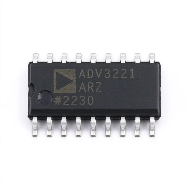
ADV3221ARZ - 800 MHz 4:1 Analog Multiplexer | Analog Devices
The Analog Devices ADV3221ARZ is a production 800 MHz, 4:1 buffered analog multiplexer in a 16-lead SOIC package. It routes one of four selectable analog inputs to a single output using high-speed, double-buffered logic control. The device is designed for high-bandwidth signal routing where short switching time, low insertion loss, controlled impedance, and low crosstalk are important. Its advertised −3 dB signal bandwidth is 800 MHz for a 200 mV p-p input and 750 MHz for a 2 V p-p input, with channel switching below 20 ns to 1% settling. An analog multiplexer is a switching IC that connects one of several input terminals to a common output path. A 4:1 device such as the ADV3221 belongs to the broader analog switch and multiplexor hierarchy, where input isolation, signal integrity, bandwidth, and control timing determine whether it can preserve a waveform during channel changes. Unlike an unbuffered passive switch, the ADV3221 includes active output drive to maintain a controlled signal path at high frequencies. Key features include 2400 V/µs slew rate, low 75 mW power consumption from ±5 V supplies, and strong video performance, including 100 MHz operation with 0.1 dB video bandwidth variation according to the supplied datasheet excerpts. The manufacturer describes the ADV3221 as a high-speed, high-slew-rate buffered 4:1 analog multiplexer, making it appropriate for video routing, instrumentation, test systems, and other wideband signal paths. The ADV3221 and closely related ADV3222 family uses double-buffered logic, allowing a new selection to be prepared before the switching interval. This architecture supports controlled break-before-make transitions and makes timing easier to coordinate in multi-channel systems. Signal amplitude can influence the quoted bandwidth, so system designers should compare performance at their actual operating amplitude rather than relying only on the headline 800 MHz figure. Typical applications include video test and measurement equipment, high-speed data-acquisition front ends, broadcast and professional video routing, and wideband communication test paths. The 16-SOIC footprint is suitable for conventional surface-mount assembly, although high-speed layouts must minimize trace lengths and provide a controlled return path. The primary design considerations are supply decoupling, controlled-impedance routing, grounding, and careful interpretation of the input and output common-mode limits. Because the manufacturer excerpt describes performance at ±5 V, engineers should verify the complete electrical limits and dual-supply requirements in the official datasheet before committing to a system design. This page consolidates verified manufacturer and distributor information, source-backed application guidance, parameter comparisons, and practical implementation notes. It adds engineering context around bandwidth, switching behavior, packaging, and sourcing while clearly separating verified specifications from parameters that still require direct datasheet confirmation.

ADV3222ARZ - 800 MHz 4:1 Analog Multiplexer | Analog Devices
The Analog Devices ADV3222ARZ is an 800 MHz, buffered 4:1 analog multiplexer with a 16-lead SOIC package. It supports dual supplies from -4.5 V to -5.5 V or +4.5 V to +5.5 V, uses double-buffered logic, and provides signal bandwidth above 800 MHz for high-speed analog routing. Its channel switching reaches 1% settling in less than 20 ns. An analog multiplexer is an interface IC that selects one of several inputs and connects that input to a common output. A 4:1 device therefore routes one of four channels through one output. In the signal-chain hierarchy, the ADV3222ARZ is a multiplexer within analog switches and multiplexers, interface ICs, and semiconductor signal-routing devices. The buffered inputs reduce source-loading effects, while double-buffered control simplifies break-before-make switching and digital sequencing. Key performance includes greater-than-800 MHz -3 dB bandwidth at 200 mV peak-to-peak, 750 MHz at 2 V peak-to-peak, a 2400 V/s slew rate, and lower than -58 dB crosstalk at 100 MHz. Isolation reaches -67 dB at 100 MHz. The supplied search data also identifies a low-power value of 75 mW at plus or minus 5 V and video performance of 0.1 dB at 100 MHz. The high-speed architecture is appropriate when preserving amplitude, edge rate, and isolation across several RF, video, pulse, or instrumentation signals matters more than minimizing switch resistance. Because the device is buffered rather than a simple low-resistance mechanical or MOS switch array, the selected channel presents an active drive path and requires careful impedance matching, termination, and control timing. Its 16-SOIC format is compatible with conventional surface-mount assembly but needs adequate high-frequency layout discipline. Typical uses include high-speed test equipment, video routing, communications instrumentation, data-acquisition front ends, and clock or pulse-signal selection. The sub-20 ns settling specification is useful in sample-and-hold and pulsed-test systems, while the 800 MHz bandwidth supports high-frequency measurement paths. Engineers should preserve symmetric routing and define unused inputs according to the manufacturer datasheet. For PCB implementation, use a continuous ground plane, short interconnects, and decoupling close to the supply pins. Terminate the selected signal into the impedance expected by the next stage, control crosstalk between adjacent channels, and verify settling at the actual amplitude and frequency. The operating voltage and unused-pin details should be checked directly against the manufacturer datasheet before layout release. This page combines manufacturer and distributor information, verified package and frequency details, sourcing links, and engineering guidance. It separates confirmed values from unavailable information and avoids presenting generic cross-reference tools as proof of pin compatibility.

ADV3224ACPZ - 750 MHz 16x8 Analog Crosspoint | Analog Devices
Analog Devices ADV3224ACPZ is a 750 MHz, 16 x 8 analog crosspoint switch in a 72-lead LFCSP-VQ package measuring 10 x 10 mm. The device provides an 8-output high-speed, nonblocking switch array with buffered inputs, programmable high-impedance outputs, and eight output amplifiers having a gain of +1. It operates from dual positive and negative 5 V supplies, consumes 0.5 W power, and drives 150 ohm loads. An analog crosspoint switch is a routing matrix that connects any selected input to any selected output without blocking other simultaneous paths. In the signal-chain hierarchy, the ADV3224ACPZ is a high-speed analog switch IC, a specialized interface device, and ultimately a semiconductor. Its nonblocking 16 x 8 architecture supports parallel routing of high-frequency analog signals where fixed point-to-point routing would be less flexible. The principal performance features include a minus 3 dB signal bandwidth greater than 750 MHz and slew rate greater than 2500 V/µs. These figures allow the device to handle wideband video, telecommunications, and other high-speed baseband signals. Buffered inputs help isolate signal sources, while programmable high-impedance outputs allow unused outputs to be placed in a high-impedance state during multi-output routing. The ADV3224ACPZ uses eight independent output amplifiers with a +1 gain. The related ADV3225 family member uses a +2 output gain, while the broader AD8110 and AD8111 devices are described as having equivalent pinouts. The architecture combines switching and output buffering in one complete crosspoint solution rather than requiring separate amplifiers for every routed channel. Typical applications include professional video routing, broadcast signal distribution, telecommunications test equipment, high-speed video measurement systems, and wideband analog signal-path switching. The 750 MHz bandwidth is particularly relevant when routing composite or component video signals, while the 16 inputs and eight outputs support matrix-style source selection. When designing a board around the ADV3224ACPZ, preserve the recommended high-speed layout topology, provide the dual ±5 V supply rails, and account for the exposed-package thermal path. The device is specified for 150 ohm loads, so output impedance, cable length, and downstream termination must be checked together to avoid reflections that could degrade bandwidth or signal integrity. This page consolidates verified manufacturer and distributor information, distinguishes documented drop-in relationships from merely similar devices, and adds practical routing, thermal, and signal-integrity guidance for engineers evaluating the ADV3224ACPZ.

ADV3226ACPZ - 750 MHz 16x16 Analog Crosspoint | Analog Devices
Analog Devices ADV3226ACPZ is a 750 MHz, 16 × 16 high-speed nonblocking analog crosspoint switch with one channel, housed in a 100-lead LFCSP-VQ package measuring 12 × 12 mm. The switch provides a signal bandwidth greater than 750 MHz, channel switching below 20 ns with 1% settling, buffered inputs, programmable high-impedance outputs, and 16 output amplifiers with a gain of +1. It operates from ±5 V supplies and can drive 150 ohm loads. An analog crosspoint switch is a matrix of independently controlled signal paths that routes one input to one output without changing the signal type. Within the semiconductor hierarchy, it belongs to the switch and multiplexer family, then to interface ICs, and finally to broader signal-path and semiconductor devices. The ADV3226 is intended for systems requiring many high-speed analog connections to be changed rapidly while preserving signal integrity. The principal features include a 16 × 16 nonblocking switch array, greater-than-750 MHz −3 dB bandwidth, less-than-20 ns switching time with 1% settling, and buffered inputs. Programmable high-impedance outputs allow unused channels to be isolated, while the output amplifiers provide unity gain. The device is designed for dual ±5 V operation and includes complete buffered input and output circuitry on one integrated circuit. Technically, the crosspoint architecture allows any input to be connected to an output while maintaining nonblocking operation. Its unity-gain output stage is suited to routing video or other wideband analog signals without intentional amplification. The ±5 V supply arrangement provides headroom for bipolar signal swings, while 150 ohm load drive capability supports practical downstream circuits. According to the Analog Devices product page, typical power consumption is 1.3 W. Typical uses include video routing, telecommunications test systems, professional video equipment, video monitoring systems, and high-speed analog test infrastructure. The 750 MHz bandwidth is appropriate for high-definition and related wideband video paths, while the sub-20 ns switching specification supports fast source selection. In these systems, the device can consolidate multiple video connections behind a controlled crosspoint rather than requiring a separate external switch per route. Designers must provide clean +5 V and −5 V rails, decouple both supplies close to the device, and preserve controlled-impedance routing around the 100-pin package. Output loading, return paths, grounding, and thermal performance require attention because the matrix can dissipate approximately 1.3 W under the stated operating conditions. The manufacturer datasheet should be used for the complete pin assignment, control protocol, and recommended layout. This page consolidates the verified manufacturer and distributor information, distinguishes the ADV3226 from related devices, and adds practical application, comparison, sourcing, and design guidance. It also makes missing electrical and pin-level details explicit rather than estimating unverified values.
ADV3227ACPZ - 750MHz 16x16 Crosspoint Switch | Analog Devices
Analog Devices ADV3227ACPZ is a production 750 MHz, 16 × 16 high-speed analog crosspoint switch IC in a 100-LFCSP-VQ 12 × 12 mm package. The device provides a nonblocking 16 × 16 switch array, buffered inputs, 16 output amplifiers with a gain of +2, programmable high-impedance outputs, and operation from dual ±5 V supplies. Its −3 dB signal bandwidth is greater than 750 MHz. An analog crosspoint switch is a routing matrix that connects any selected input signal to any selected output under digital control. This product type belongs to the broader hierarchy of switch IC, interface IC, signal-routing IC, and semiconductor. Unlike a mechanical relay network, it provides electronic routing with high bandwidth, buffered signal paths, programmable output impedance, and switching times below 20 ns with 1% settling. The principal features of the ADV3227ACPZ include a 16 × 16 nonblocking array, a gain of +2 on every output, and a complete buffered-input solution. The architecture can drive 150 Ω loads and consumes 1.3 W. Its 750 MHz bandwidth makes it suitable for routing high-speed analog and video signals while retaining useful isolation between the selected source and destination. Technically, the ADV3227 belongs to the ADV3226/ADV3227 family. The manufacturer describes its pinout as functionally equivalent to the AD8114 and AD8115, although package size and exact footprint requirements must be checked before substitution. The principal difference between ADV3226 and ADV3227 is output gain: ADV3226 has a gain of +1, while ADV3227 uses output amplifiers with a gain of +2. Typical applications include video routing, telecommunications infrastructure, professional broadcast equipment, test and measurement systems, and high-speed signal-distribution cabinets. The nonblocking architecture allows simultaneous routing activity across independent matrix intersections, while the buffered inputs help maintain signal integrity when driving terminated analog lines. When laying out a design, treat the ±5 V rails, analog signal paths, control inputs, and exposed package ground as separate layout concerns. Keep high-speed routes short, provide the required bypass capacitance at the supply pins, and maintain controlled return paths beneath the matrix. Before using another high-speed switch, verify package dimensions, pin assignments, control logic, output impedance, gain, and settling requirements rather than relying only on bandwidth. This page combines the verified manufacturer and distributor data for the ADV3227ACPZ with practical routing considerations, comparison parameters, and honest drop-in-replacement analysis. It distinguishes true same-package options from related devices that are functionally similar but require board-level verification.
ADV3228ACPZ - 750MHz 8x8 Crosspoint Switch | Analog Devices
The Analog Devices ADV3228ACPZ is a high-speed 8 × 8 analog crosspoint switch with a 750 MHz −3 dB large-signal bandwidth and 2500 V/µs slew rate. It is packaged in a 72-lead LFCSP-VQ package measuring 10 mm × 10 mm. The device provides a complete buffered-input crosspoint solution for routing high-bandwidth analog signals across eight inputs and eight outputs, including telecommunications, video, broadcast, test-and-measurement, and instrumentation systems. An analog crosspoint switch is an integrated routing matrix that connects any selected input to any selected output while providing controlled impedance and gain. The ADV3228 combines eight high-speed, nonblocking switch arrays, buffered inputs, programmable high-impedance outputs, and eight output amplifiers with +1 gain. Its architecture makes it useful where a board must route multiple wideband channels without relying on discrete relays or lossy passive networks. The device is specifically identified as pin-compatible and functionally equivalent to the AD8108 and AD8109, and is drop-in compatible with the ADV3224 and ADV3225 16 × 8 array family according to the manufacturer product-page information. Key performance features include a 750 MHz −3 dB large-signal bandwidth for ADV3228, 2500 V/µs slew rate, operation from ±5 V supplies, and the ability to drive 150 Ω loads. Programmable high-impedance outputs allow selected output channels to be placed in a high-impedance state, which can support paralleling or system-level routing strategies. The buffered-input architecture and output amplifiers provide a complete routing solution rather than requiring external signal-conditioning stages. The ADV3228ACPZ is suitable for video routing, telecommunications equipment, broadcast systems, high-speed test equipment, and professional audio or instrumentation designs. The 72-lead LFCSP-VQ package supports dense PCB layouts, while the exposed-pad construction provides an important thermal path for power dissipation. Designers should pay close attention to supply bypassing, controlled-impedance routing, thermal-pad layout, and the datasheet’s recommended input and output termination networks. When selecting a replacement, verify the exact ACPZ package, pinout, gain configuration, supply arrangement, and bandwidth requirements. The ADV3229 has +2 gain rather than the ADV3228’s +1 gain, while ADV3224 and ADV3225 belong to the related 16 × 8 family. For existing designs that require the ADV3228’s exact gain and footprint, the manufacturer-documented compatible parts provide the safest replacement path. This page combines verified manufacturer and distributor information with practical design guidance and a structured comparison of documented alternatives.
ADV3229ACPZ - 750 MHz 8x8 Crosspoint Switch | Analog Devices
Analog Devices ADV3229ACPZ is a high-speed, nonblocking 8 x 8 analog crosspoint switch with a 750 MHz bandwidth, +2 gain output amplifiers, and a 72-lead LFCSP-VQ package measuring 10 x 10 mm. It supports buffered inputs, programmable high-impedance outputs, and drives of 150 ohm loads while operating from positive and negative 5 V supplies. An analog crosspoint switch is a multi-input, multi-output routing matrix that connects any selected input channel to any selected output channel without requiring the inactive channels to terminate. Within the semiconductor hierarchy, the ADV3229ACPZ is an analog switch IC, an interface IC, and a signal-routing device for high-frequency video, telecommunications, broadcast, and test equipment. Its nonblocking architecture allows supported channels to remain active while other crosspoint routes change. Key features include an 8 x 8 switch array, eight buffered inputs, eight programmable high-impedance outputs, and eight output amplifiers configured for a gain of +2. The device is specified for 150 ohm loads and low power consumption of 0.5 W. According to the Analog Devices ADV3228/ADV3229 data sheet, its large-signal bandwidth is 750 MHz and its slew rate is 2500 V/us. Technically, the ADV3229 integrates routing switches, input buffers, output amplifiers, and output-disconnect functions into one high-speed analog matrix. The +2 output gain differentiates it from the otherwise closely related ADV3228, which uses +1 gain. The data sheet also identifies the ADV3229 as pinout- and functionally equivalent to the AD8108 and AD8109, making those legacy devices important references when evaluating board compatibility. Typical uses include professional video routing, broadcast video distribution, telecommunications test systems, high-definition signal routing, and instrumentation requiring repeatable high-bandwidth channel selection. The buffered inputs help isolate upstream sources, while the programmable output high-impedance states allow unused outputs to be isolated from driven channels. Designers should verify control-logic levels, exposed-pad grounding, bypass-capacitor placement, and signal-integrity performance on the target board. The 10 x 10 mm land pattern and high-speed analog routing require short connections, a continuous ground reference, and careful control of supply-return paths. Because the ADV3229 uses dual-rail supplies, both positive and negative rails must be present with appropriate decoupling. This page consolidates manufacturer features, distributor pricing, verified source links, same-family drop-in alternatives, and practical selection guidance. It also distinguishes confirmed pin-compatible options from legacy functionally equivalent devices so engineers can verify every footprint, gain, and control requirement before redesigning an existing PCB.
ADV7171KS - 10-Bit PAL/NTSC Video Encoder | Analog Devices
The Analog Devices ADV7171KS is an integrated digital PAL/NTSC video encoder with a 10-bit DAC and advanced power management, packaged in a 44-lead MQFP. According to the manufacturer product page, it converts Digital CCIR-601 4:2:2 8-bit or 16-bit component video data into a standard analog baseband television signal compatible with worldwide standards. The encoder is designed for DVD playback systems, portable video equipment, digital still cameras, laptop PCs, video games, and PC video or multimedia systems. A digital video encoder is an interface and signal-conversion IC that accepts parallel digital video, applies encoding and color-processing functions, and generates composite or component analog video suitable for display equipment. Its role in the signal chain is between a digital video source and an analog display or broadcast interface. The ADV7171 family supports serial control through a 2-wire I2C-compatible interface and uses two slave addresses, allowing configuration of operating modes and encoder functions from a host controller. The key verified feature set includes Digital CCIR-601 4:2:2 input support in either 8-bit or 16-bit formats, a 10-bit DAC, PAL and NTSC encoding capability, and advanced power management. The Analog Devices family description identifies the device as an integrated digital video encoder rather than a general-purpose processor. Its 44-lead MQFP package provides a defined gull-wing footprint for conventional surface-mount PCB assembly and is available in industrial-temperature component listings. The ADV7171KS is appropriate when a design must preserve a digital video source while producing standard analog baseband output. The serial control interface simplifies integration with source-specific firmware, while the dedicated video encoder reduces the need for external DAC and encoding circuitry. Engineers should still verify clocking, sync polarity, pixel clock relationships, output loading, power sequencing, and analog video quality against the complete manufacturer datasheet before releasing a production layout. Typical applications include DVD playback systems, portable video equipment, digital still cameras, laptop computers, video games, and PC video or multimedia products. In these systems, the encoder can convert decoded digital video into PAL or NTSC-compatible analog signals for downstream display or capture equipment. The dedicated encoder also supports integration into compact consumer products where board area and external component count are important. A key design consideration is that analog baseband video requires careful PCB layout and signal-integrity control. Keep the encoder clock and digital-video traces away from sensitive output paths, provide clean power and ground connections, and follow the manufacturer’s recommended decoupling and output-network details. Because the supplied web data does not expose the complete electrical timing table, pin names, or exact operating limits, those values should not be inferred from generic video-encoder specifications. This page consolidates verified manufacturer and distributor information, including the ADV7171KS application context, package identity, family capabilities, and replacement-search results. It is intended to support component selection and engineering research while clearly separating verified facts from parameters that still require confirmation in the complete ADV7170/ADV7171 datasheet.

ADV7171KSU 10-Bit PAL/NTSC Video Encoder | Analog Devices
Analog Devices ADV7171KSU is an integrated 10-bit digital video encoder that converts ITU-R BT.601/656 YCrCb 4:2:2 component data into standard PAL or NTSC analog baseband video. The device provides four video DAC outputs and is supplied in a surface-mount 44-pin TQFP package measuring 10 mm by 10 mm. Its primary function is to bridge a digital video source and legacy analog composite, S-Video, or component outputs. A video encoder is a signal-conversion semiconductor that accepts digital pixel data and generates an analog waveform accepted by PAL or NTSC display equipment. Within the product hierarchy, the ADV7171 is an interface IC and video encoder rather than a processor or display driver. The corresponding digital-video-to-analog-video conversion stage sits between a video source, such as a DVD controller or multimedia processor, and an analog video connector or display. According to the Analog Devices ADV7171 product page, the encoder supports 8-bit or 16-bit CCIR-601 4:2:2 component video input. Its four 10-bit DACs support PAL and NTSC generation, while its digital video input follows the BT.601/656 format identified in the provided product information. This integration reduces the need for external video DACs when a design requires both S-Video and composite or additional analog video outputs. The ADV7170 and ADV7171 family is positioned for high-performance DVD playback, portable video equipment, digital still cameras, laptop computers, video games, and PC video or multimedia systems. The supplied search data does not provide verified clock frequency, power-supply range, output voltage resolution, operating temperature, timing limits, or package dimensions beyond the 10 mm by 10 mm TQFP description, so those values are not inferred here. The main engineering concern is interface compatibility rather than power conversion. The source must supply correctly timed BT.601/656 YCrCb data, the PCB must route high-speed digital video signals without excessive distortion, and analog outputs must be terminated according to the selected PAL or NTSC standard. The exact clocking, synchronization, control-register, and DAC configuration procedure must be taken from the manufacturer data sheet rather than inferred from the order code. For procurement, ADV7171KSUZ and ADV7171KSUZ-REEL appear in the supplied cross-reference results as the same 44-pin device with compatible terminals and characteristics, but the KSUZ order codes may represent ordering or reel-packaging conventions rather than five distinct functional alternatives. This page therefore distinguishes verified function-level choices from packaging suffixes and does not present reel-code variants as separate engineering options. This page consolidates the supplied manufacturer description, distributor package information, cross-reference findings, application guidance, and unresolved-data warnings. It is intended to support engineering selection and sourcing while directing readers to the manufacturer data sheet for authoritative electrical limits, pin functions, register definitions, and timing specifications.