Logic ICs
Products (88)

SN74LVC374A-Q1 - Octal D Flip-Flop, 3-State | Texas Instruments
The Texas Instruments SN74LVC374A-Q1 is an automotive-catalog octal edge-triggered D-type flip-flop with 3-state outputs, operating from a 1.65V to 3.6V supply (designed for 2.7V to 3.6V VCC operation) and available in 20-pin surface-mount packages including SOIC-20 (DW) and TSSOP-20 (PW). An octal D-type flip-flop is a sequential logic IC in the 74-series logic family that captures eight data bits simultaneously on the rising edge of a clock signal and holds them until the next clock edge. Within the logic hierarchy, it belongs to the flip-flop/latch category of CMOS integrated circuits, which sit inside the broader domain of digital logic ICs and semiconductor components. The 3-state outputs allow the device to be electrically disconnected from a shared bus, enabling multi-drop bus architectures. Key features include 3-state outputs designed specifically for driving highly capacitive or relatively low-impedance loads, 5.5V-tolerant input pins allowing safe interfacing with 5V logic systems, and typical output ground bounce (VOLP) and VOH undershoot (VOHV) specifications provided at VCC = 3.3V, 25C. As a high-drive CMOS device, it delivers 32 mA of drive current at 3.3V, making it ideal for driving multiple outputs and for high-speed applications up to 100 MHz, according to TI's SNx4LVC374A literature. The Q1 automotive-catalog variant is qualified for automotive environments and suits AEC-relevant designs. The architecture uses edge-triggered master-slave storage with a common clock (CP) pin and an active-low output-enable (OE) pin that controls all eight 3-state outputs independently of the clock. Typical applications include automotive body electronics, bus-interface buffering and data retention, register banks in instrumentation, and memory address/data latching where a shared 3-state bus is required. Design tip: tie the OE pin high through a pull-up resistor at power-up to keep the bus disconnected until the clock and data lines are stable, avoiding bus contention during system initialization.
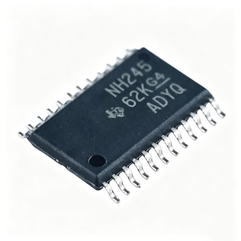
SN74LVC8T245PWR - 8-Bit Dual-Supply Level Translator | TI
The Texas Instruments SN74LVC8T245PWR is an 8-bit dual-supply bus transceiver with configurable voltage translation and 3-state outputs, packaged in a 24-pin TSSOP (PW) with Tape and Reel delivery. Both the VCCA and VCCB ports operate over the full 1.65V to 5.5V supply range, enabling bidirectional level translation between any combination of 1.8V, 2.5V, 3.3V, and 5V logic domains. A bus transceiver is a digital logic IC that moves data bidirectionally between two buses, with direction (DIR) and output-enable (OE) controls providing the handshake. The SN74LVC8T245 belongs to the voltage-level translator / logic IC hierarchy and is a member of the TI Widebus+ family, solving the classic mixed-voltage problem in systems where MCUs, FPGAs, and peripherals run on different rails. Key features include the fully configurable dual-rail architecture, 3-state outputs for bus sharing, mixed-mode signal operation (5V-tolerant I/O with reduced supply), and Ioff plus power-up 3-state support that blocks damaging backflow current during partial power-down and hot-insertion events. DIR and OE are referenced to VCCA, simplifying control-logic design. Technically, the device uses two independent supply-referenced port circuits with low-impedance LVC output drivers. The typical data rate of 100 Mbps supports SPI, I2C, UART, and parallel bus translation while preserving signal integrity with up to 15 pF load capacitance. Inputs accept voltages up to 5.5V regardless of supply level. Typical applications include level shifting for SD and SIM card interfaces, sensor and memory modules, 3.3V-to-5V industrial control I/O, and FPGA/CPLD I/O-bank adaptation to external peripherals. Design tip: decouple both VCCA and VCCB with 0.1uF ceramic capacitors placed close to the pins, tie OE to its proper logic level to avoid a 3-state bus at power-up, and set DIR according to data flow direction. Prices as of 2026-08-30.

SN74LVC8T245QPWRQ1 - 8-Bit Auto Level Shifter | Texas Instruments
The Texas Instruments SN74LVC8T245QPWRQ1 is an automotive-grade, 8-bit dual-supply bus transceiver with configurable voltage translation and 3-state outputs, supplied in a 24-pin TSSOP (PW) package. It is AEC-Q100 qualified for operation from -40C to +125C, making it suited for harsh automotive and industrial environments. A dual-supply bus transceiver is a logic component that moves data between two digital buses operating at different voltage levels. In the power-management and signal-chain hierarchy, it belongs to the level-translator family within the broader logic IC category. The SN74LVC8T245-Q1 uses two independent supply rails, VCCA and VCCB, each operable from 1.65V to 5.5V, enabling bidirectional translation between any two voltage domains, such as 1.8V MCUs communicating with 3.3V or 5V peripherals. Key features include direction-controlled (DIR) and output-enable (OE) pins supplied by VCCA, 3-state outputs for bus sharing, Ioff and power-up 3-state support for hot-insertion safety, and 5.5V-tolerant inputs. The device transmits data from A to B when B-port outputs are active, and from B to A otherwise, supporting asynchronous two-way bus communication with configurable translation on every bit. Architecturally, the device belongs to the TI LVC (Low-Voltage CMOS) family and the Widebus+ 8-bit format, combining fast propagation times at 3.3V with robust mixed-mode signal operation on all ports. Data-sheet-level design freedom comes from independent VCCA/VCCB pinout ordering, which simplifies PCB routing between voltage domains. Typical applications include automotive body and gateway ECUs translating MCU GPIO to CAN/LIN transceiver logic levels, infotainment and display module bus isolation, and industrial PLC I/O modules interfacing 3.3V controllers with 5V sensors. The 3-state outputs let multiple transceivers share one bus without contention. Design tip: tie OE high or low through a pull resistor at power-up to prevent bus contention, since the control pins are referenced to VCCA; ensure VCCA ramps before the uncontrolled bus is driven. This page synthesizes distributor pricing, drop-in alternatives, and practical design notes not found in the manufacturer datasheet. Pricing shown as of 2026-09-01.
SN74LVTH16374-EP - 3.3V 16-Bit D Flip-Flop EP | Texas Instruments
The Texas Instruments SN74LVTH16374-EP is an Enhanced Product (EP) version of the 3.3-V ABT 16-bit edge-triggered D-type flip-flop with 3-state outputs. Designed for low-voltage 3.3-V VCC operation, the device provides TTL-level interface capability to 5-V system environments, making it well suited for defense, aerospace, and medical applications. It integrates sixteen positive-edge-triggered D-type flip-flops with common clock (CP) and output-enable (OE) controls in a space-saving 48-pin SSOP/TSSOP-style surface-mount package. A D-type flip-flop is a fundamental sequential logic element in the CMOS/TTL logic IC family hierarchy: it is a bistable storage circuit that captures the value at its D input on the rising edge of a clock signal and holds it at the Q output until the next clock edge. Sixteen-bit registered buffers like the SN74LVTH16374-EP belong to the broader categories of bus interface flip-flops, logic ICs, and digital semiconductors, providing pipeline registers, data latching, and bus isolation functions in digital systems. Key features include EP (Enhanced Product) qualification supporting defense, aerospace, and medical applications, 3.3-V operation with 5-V TTL-compatible inputs, 3-state outputs for bus-oriented applications, and ABT (Advanced BiCMOS Technology) combining CMOS low power with TTL drive capability and speed. The device is qualified against the standard SN74LVTH16374, with identical electrical behavior and pinout. Technically, the LVTH family uses BiCMOS process technology to achieve fast edge rates, balanced drive, and low dynamic power. The 3-state outputs place all sixteen Q outputs into a high-impedance state when OE is high, allowing multiple devices to share a common data bus. Edge-triggered clocking on the positive clock edge simplifies synchronous pipeline design versus level-sensitive latches. Typical applications include pipeline data registers in space-constrained avionics and defense electronics, bus isolation and buffering in medical imaging equipment, address/data latching in industrial control, and general-purpose 16-bit synchronous storage where EP-level reliability documentation is required. Design consideration: tie unused inputs to VCC or GND to prevent floating-node oscillation, and always bypass VCC with a 0.1-uF ceramic capacitor close to the device. Verify availability as of 2026-08-30 before committing to a variant.
TLV3801 - 225ps LVDS High-Speed Comparator | Texas Instruments
The Texas Instruments TLV3801 is a 225-ps high-speed comparator with complementary LVDS outputs, operating from a single 2.7 V to 5.25 V supply or a split supply of ±1.35 V to ±2.625 V, with a toggle frequency up to 3 GHz. It is packaged in an 8-pin WSON (DSG) 2x2 mm package for space-constrained designs. A comparator is an electronic circuit that compares two input voltages and outputs a digital signal indicating which is larger. The TLV3801 belongs to the high-speed comparator subclass, optimized for minimal propagation delay and high toggle rates. It sits within the analog-to-digital interface hierarchy, bridging analog signals to LVDS digital logic levels for downstream FPGAs and CPUs. Key features include a 225-ps propagation delay, complementary LVDS outputs that reduce EMI and suppress common-mode noise, and low power consumption of about 6.5 mW at 3.3 V. An enable pin supports power management and rail sequencing. The LVDS output stages drive standard LVDS inputs directly at up to 3 GHz toggle frequency. The device is built on a bipolar process with a differential input stage and LVDS output drivers, delivering deterministic, low-jitter switching. It is specified over the industrial temperature range of -40C to +125C, and an automotive-grade TLV3801-Q1 variant is available for AEC-Q100 applications. Typical applications include LIDAR pulse detection, where every nanosecond of propagation delay affects range resolution, high-speed differential line receivers for data transmission, and optical sensor modules. Clock recovery and fast data acquisition systems also benefit from the high toggle rate. Design tip: terminate the LVDS outputs with 100 ohm differential impedance and decouple each supply pin with 0.1 uF capacitors placed as close to the device as possible to preserve signal integrity.

TMUX8108PWR - 100V Flat RON 8:1 Analog MUX | Texas Instruments
The Texas Instruments TMUX8108PWR is a 100-V rated, flat on-resistance, single 8:1 (single-ended) analog multiplexer housed in a 16-pin TSSOP (PWR) package. It delivers a consistent on-resistance of approximately 50 ohm across the full analog signal range and supply conditions, supports single, dual, or asymmetric supplies up to 100 V total, and features latch-up immunity plus 1.8-V-compatible logic inputs. An analog multiplexer is a switching IC that routes one of several analog signal inputs to a single common output under digital control, forming part of the broader family of analog switches within signal-chain and power-management integrated circuits. Multiplexers are essential wherever many sensors, test points, or signal sources share a single downstream amplifier, ADC, or measurement instrument, saving board area, cost, and channel count on data converters. Key differentiating features of the TMUX8108 include its 100-V maximum supply rating, far above the 36 V ceiling of conventional CMOS multiplexers, its flat RON characteristic that minimizes signal-dependent gain error across the signal range, and latch-up immunity that protects the device in harsh industrial and medical environments where voltage transients are common. Control logic accepts 1.8 V, 3.3 V, and 5 V levels and, according to TI product documentation, logic inputs can be driven as high as 48 V, giving designers exceptional flexibility in interfacing with mixed-voltage systems. The device supports bidirectional analog and digital signals on the source (Sx) and drain (D) pins and provides break-before-make switching to prevent momentary channel shorting. Consistent analog parametric performance is maintained across the entire supply voltage range, simplifying design reuse from low-voltage to high-voltage systems. Typical applications include industrial programmable logic controller analog input modules, battery test and formation equipment, medical diagnostic instrumentation front ends, and automated test equipment (ATE) signal routing, all of which benefit from the high supply ceiling and rugged latch-up immunity. Designers should observe the total supply constraint of 100 V across VDD and VSS and verify signal swing stays within the supply rails; the flat RON makes channel-to-channel matching predictable even at high common-mode voltages. This page synthesizes verified distributor data, drop-in alternatives, and practical design guidance not found in the manufacturer datasheet, with pricing referenced as of 2026-09-03.
TMUX8108RUMR - 100V 8:1 Analog Mux, 48Ohm | Texas Instruments
The Texas Instruments TMUX8108RUMR is a 100 V, flat RON, single 8:1 analog multiplexer with latch-up immunity and 1.8 V logic compatibility, housed in a 16-pin WQFN (4x4 mm, RUM) package with a typical on-resistance of 48 ohm. An analog multiplexer is a switching IC that routes one of several analog input signals to a single output channel under digital control. Within the signal-chain hierarchy, it sits between sensors or signal sources and amplifiers, ADCs, or measurement front ends, acting as a electronically controlled switch matrix. Multiplexer ICs belong to the broader family of analog switches, which themselves are part of the interface and signal-routing layer of power and data acquisition systems. Key features of the TMUX8108 include support for dual, single, or asymmetric supplies up to a maximum supply voltage of 100 V, low and flat on-capacitance behavior across the signal range, low OFF leakage current, and robust latch-up immunity that protects the device in harsh industrial environments. The 1.8 V-compatible logic inputs allow direct interfacing with modern low-voltage microcontrollers and FPGAs without level shifting. Technically, the TMUX810x family provides consistent analog parametric performance across the entire supply voltage range, meaning RON, leakage, and switching behavior remain stable whether the part runs from plus/minus supplies or a single high-voltage rail. This flat RON characteristic minimizes signal-dependent gain error in precision measurement paths, a common weakness of older high-voltage mux architectures. Typical applications include industrial programmable logic controller (PLC) analog input modules, automated test equipment (ATE) signal routing, battery test and formation systems operating at high cell voltages, and high-voltage data acquisition front ends. The 8:1 configuration suits multi-channel monitoring where several sense points share one precision ADC. A key design consideration is supply configuration: because the device accepts up to 100 V total supply, designers should verify signal swing stays within the supply rails and account for on-resistance times channel-current voltage drops in error budgets. This page synthesizes distributor pricing, drop-in alternative analysis, and practical design notes not found in the manufacturer datasheet, giving engineers a complete selection resource in one place.

TS3A5018QPWRQ1 - 10-Ohm Quad SPDT Analog Switch | Texas Instruments
The Texas Instruments TS3A5018QPWRQ1 is an automotive-qualified (AEC-Q100) quad single-pole double-throw (SPDT) analog switch designed to operate from a 1.8V to 3.6V supply. Packaged in a 16-pin TSSOP (PW), it provides four independent SPDT switches with a low 10-ohm on-resistance, handling both digital and analog signals up to V+ in either direction. An analog switch (also called an analog multiplexer/demultiplexer or bidirectional switch IC) is a semiconductor device that routes analog or digital signals through a MOSFET transmission gate controlled by a digital select input. Analog switches sit within the broader signal-routing hierarchy: analog switch IC -> signal multiplexer -> interface and switching IC -> analog signal chain. They are fundamental building blocks wherever a processor must dynamically reconfigure signal paths without degrading signal integrity. Key features of the TS3A5018QPWRQ1 include the low 10-ohm typical on-resistance, wide 1.8V to 3.6V single-supply operation suited to battery-powered and low-voltage systems, full rail-to-rail signal handling, and break-before-make switching that prevents momentary shorting of signal sources. The Q1 suffix denotes AEC-Q100 qualification for automotive environments, with an extended operating temperature range supporting under-hood and body electronics applications. The device uses CMOS transmission-gate architecture, which keeps on-resistance relatively flat across the signal range and minimizes signal distortion for audio and data-routing tasks. Because signals up to V+ can pass in either direction, the switches work equally well for multiplexing and demultiplexing, such as sharing a codec between microphone and headset paths or switching antenna and test signals. Typical applications include automotive infotainment audio routing, battery-management cell-monitoring multiplexing, portable instrument signal switching, and general-purpose I/O expansion in industrial control boards. Design tip: minimize RON signal loss by keeping source impedance low, and always provide a solid V+ decoupling capacitor (0.1uF close to the pin). Remember that the analog signal range is limited to the 0V-to-V+ supply window; signals outside this range must be blocked or level-shifted.
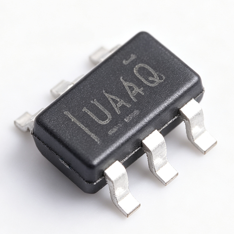
TS5A3159QDBVRQ1 - 1Ω SPDT Analog Switch AEC-Q100 | TI
The Texas Instruments TS5A3159QDBVRQ1 is an automotive-qualified (AEC-Q100) single-pole double-throw (SPDT) 2:1 analog switch with 1Ω typical ON-state resistance (1.3Ω max), operating from a 1.65V to 5.5V supply in a 6-pin SOT-23 (DBV) package. An analog switch is a semiconductor device that routes or gates analog and digital signals under the control of a logic-level input. Within the signal-chain hierarchy, the SPDT analog switch sits in the analog switches and multiplexers family, below large multiplexer arrays and alongside transmission-gate logic. An SPDT device connects one common (COM) terminal to either of two throw terminals (NO or NC), making it the fundamental building block of signal routing and redundancy switching. Key features include break-before-make switching, which prevents momentary channel shorting during transition and eliminates signal distortion when a signal source moves between paths; an excellent total harmonic distortion (THD) specification that preserves audio and precision-signal integrity; and low ON-resistance matching and flatness, which minimize signal error across the input range. The device operates from a single 1.65V to 5.5V supply, compatible with 1.8V, 2.5V, 3.3V, and 5V logic systems. The switch core uses a low-charge-injection MOS transmission-gate architecture with approximately 8pF typical ON capacitance (per TI family data), limiting high-frequency insertion loss in data and RF routing paths. The digital IN pin is logic compatible across the full supply range, and the -Q1 suffix denotes AEC-Q100 qualification with -40C to +125C operation for automotive environments. Typical applications include automotive audio source selection, sensor-signal multiplexing in battery-management and body-control modules, UART/SPI/SMBus line sharing, and general-purpose signal gating in industrial systems. The 2.9mm x 1.6mm SOT-23-6 footprint suits densely populated boards. Design tip: terminate or AC-ground unused throw terminals to reduce crosstalk, and place the device close to the signal source to minimize parasitic trace capacitance. This page synthesizes distributor pricing, drop-in alternatives, comparison tables, and practical design notes not found in the manufacturer datasheet.

TS5A63157 - 10-Ohm SPDT Analog Switch 1.65-5.5V | TI
The Texas Instruments TS5A63157 is a single-pole, double-throw (SPDT) analog switch, also described as a 2:1 multiplexer/demultiplexer, designed to operate from a 1.65 V to 5.5 V supply. It handles both digital and analog signals with a low on-state resistance of approximately 10-12 ohms and comes in a 6-pin SC-70 (SOT, SC70-6, DCK) surface-mount package. An analog switch is a type of signal-routing IC in the broader family of multiplexers and switches within the semiconductor component hierarchy. Unlike a relay or mechanical switch, an analog switch uses CMOS transmission gates to route signals with low distortion, fast switching times, and no moving parts, making it fundamental to signal-chain design in portable and battery-powered systems. Key features include overshoot and undershoot voltage protection: the device senses voltage events at the I/Os and responds by preventing voltage differentials from developing and turning the switch on. It also provides isolation in powered-off mode (leakage specified at 0 when V+ = 0), break-before-make switching, 5-V tolerant control inputs, low charge injection, and excellent on-state resistance flatness. Technically, the TS5A63157 uses a CMOS switch architecture with integrated protection circuitry, allowing it to survive I/O faults that would damage unprotected switches. The powered-off isolation makes it ideal for hot-swap and battery-powered systems where rails may be sequenced or removed while signal lines remain connected. Typical applications include battery-powered portable devices, audio signal routing, hot-swap USB and peripheral switching, and multiplexing sensor or test signals in instrumentation. Priced at roughly $0.34 in single units as of 2026-08-30 per distributor data, it is also cost-effective for high-volume designs. Design tip: ensure the control input logic level is compatible with the V+ rail; control inputs are 5-V tolerant regardless of supply, and the break-before-make timing prevents momentary shorting of the two switch paths during transitions.
TXB0104RUTR - 4-Bit Bidirectional Level Shifter | Texas Instruments
The Texas Instruments TXB0104RUTR is a 4-bit bidirectional voltage-level translator with automatic direction sensing and ±15-kV ESD protection (Human Body Model), housed in a 12-pin UQFN (RUT) package measuring 1.7 mm x 2.0 mm. It translates signals between a low-voltage A port operating from 1.2 V to 3.6 V and a higher-voltage B port from 1.65 V to 5.5 V (VCCA <= VCCB), supporting data rates up to 100 Mbps. A voltage-level translator, also called a level shifter, is an integrated circuit in the logic-translation family that enables communication between digital devices operating at different supply voltages. In mixed-voltage systems, a 1.8 V or 3.3 V MCU may need to interface with 5 V peripherals; translators convert logic levels bidirectionally while protecting low-voltage silicon. The TXB0104 belongs to the auto-direction-sensing translator family, eliminating direction-control pins and simplifying both PCB design and firmware. Key features include per-channel automatic direction sensing, ±15-kV HBM ESD protection on all pins, tri-state outputs with an output-enable (OE) pin for bus isolation, and an operating temperature range of -40C to +85C. Low quiescent current and the tiny UQFN footprint suit space-constrained portable designs. Architecturally, the TXB0104 uses a one-shot edge accelerator that speeds rising and falling edges, enabling 100 Mbps operation with low static power. The A port tracks VCCA and the B port tracks VCCB. Partial power-down via OE and Ioff-style isolation make it suitable for hot-insertion environments. Typical applications include SPI, UART, and push-pull GPIO level shifting between MCUs, sensors, SIM card and SD card interfaces, and memory peripherals in mobile, industrial, and consumer products. The push-pull driver topology is not recommended for open-drain buses such as I2C or 1-Wire, as confirmed in TI E2E forum threads. Design tip: power VCCA before VCCB, place 0.1 uF bypass capacitors close to both supply pins, and use the OE pin for sequencing. For open-drain buses, consider TXS0104E instead.

TXB0108PWR - 8-Bit Bidirectional Level Shifter 100Mbps | TI
The Texas Instruments TXB0108PWR is an 8-bit bidirectional voltage-level translator with auto-direction sensing and +/-15-kV ESD protection, housed in a 20-pin TSSOP (PW) package. It translates signals between a 1.2V to 3.6V A port and a 1.65V to 5.5V B port (VCCA <= VCCB), with data rates up to 100 Mbps, making it ideal for mixed-voltage digital systems. A voltage-level translator is a logic IC that enables communication between devices operating at different supply voltages, such as a 1.8V microcontroller and a 3.3V or 5V peripheral. It sits in the hierarchy of logic ICs under level shifters (translators), which are essential in multi-voltage digital systems alongside buffers and bus transceivers. The TXB0108PWR uses auto-direction sensing, eliminating the need for a direction control pin and reducing firmware complexity. Key features include auto-direction sensing, +/-15-kV ESD protection (HBM), a 100 Mbps maximum data rate, and a VCC isolation feature: if either VCC input is at GND, all outputs enter the high-impedance state, enabling partial-power-down operation with Ioff support. The device operates from -40C to +85C. Technically, the TXB0108 uses a one-shot architecture that accelerates low-to-high transitions to achieve 100 Mbps. It is designed for push-pull (totem-pole) CMOS drivers only; for open-drain buses such as I2C, TI recommends the TXS0108E. Output drive is intentionally weak (internal 4 kOhm series resistors), so heavy capacitive loads above ~70 pF reduce achievable speed. Typical applications include 1.8V-to-3.3V microcontroller-to-sensor interfaces, SD card level shifting, UART/SPI signal translation, and FPGA configuration buses. The 100 Mbps capability suits high-speed SPI and UART links. Design tip: ensure VCCA <= VCCB, drive all eight channels push-pull, and place 0.1uF decoupling capacitors close to both VCCA and VCCB pins with short traces for signal integrity.

TXB0108QPWRQ1 - 8-Bit Auto-Direction Level Translator | TI
The Texas Instruments TXB0108QPWRQ1 is an automotive-qualified (AEC-Q100) 8-bit bidirectional voltage-level translator with auto-direction sensing and ±15kV ESD protection, packaged in a 20-pin TSSOP (PW). Port A supports 1.2V to 3.6V supplies while Port B supports 1.65V to 5.5V, enabling translation between any two logic rails in these ranges. A voltage-level translator (also called a logic level shifter) is an interface IC that enables digital devices operating on different supply rails - such as a 1.8V microcontroller and a 5V peripheral - to communicate reliably. Translators sit within the broader logic IC family, under interface and signal-conversion devices, and are essential wherever mixed-voltage systems coexist on one board. Key features include auto-direction sensing that eliminates the need for a direction-control pin, an output-enable (OE) input that places all I/O in Hi-Z when low, and ±15kV IEC ESD protection on I/O pins. The TXB0108-Q1 uses TI TXB-type push-pull architecture, delivering symmetric drive on both ports without external pull-up or pull-down resistors, and supports data rates up to 100 Mbps for 1.2V to 3.6V translation per the datasheet. The device operates from -40C to +125C (AEC-Q100 Grade 1), making it suitable for harsh automotive environments. Its TSSOP-20 package is standard, easy to assemble, and compatible with the commercial TXB0108PWR footprint for design reuse. Typical applications include automotive infotainment and cluster modules interfacing 3.3V MCUs with 5V sensors, mixed-voltage SPI/I2C-style GPIO expansion, industrial control modules, and portable mixed-signal systems bridging 1.8V and 5V rails. Design note: the TXB architecture has relatively weak output drive (not intended for bus-holding or heavy loads); avoid using it for I2C open-drain buses - the TXS family is a better fit. Pull OE low during power sequencing to prevent bus contention.

TXS0102DCUR - 2-Bit Bidirectional Level Shifter | Texas Instruments
The Texas Instruments TXS0102DCUR is a 2-bit bidirectional voltage-level translator designed for open-drain and push-pull applications. It enables digital switching compatibility between mixed-voltage systems using two separate configurable power-supply rails: the A ports support 1.65V to 3.6V while tracking VCCA, and the B ports support 2.3V to 5.5V while tracking VCCB. The device comes in an 8-pin VSSOP (DCU) package and operates from -40C to +85C. A voltage-level translator, also called a level shifter, is an integrated circuit that allows communication between components operating at different voltage levels. In mixed-voltage systems combining 3.3V microcontrollers with 5V sensors, or 1.8V logic with 3.3V peripherals, level shifters ensure logic high and low signals are correctly interpreted across voltage domains. The TXS0102 belongs to the bidirectional translator class, which shifts signals in both directions without a direction-control signal, simplifying design and reducing pin count within the broader logic IC and voltage-translation hierarchy. Key features include auto-direction sensing with no direction pin required, maximum data rates of 24 Mbps for push-pull and 2 Mbps for open-drain applications, and support for I2C, SMBus, and UART interfaces. A one-shot accelerator architecture speeds up rising edges even with capacitive loads. The OE pin, when low, places outputs in a high-impedance state for power sequencing and bus isolation. Technically, the TXS0102 uses a pass-gate architecture with integrated pull-up resistors on both A and B ports. When a line is driven low the pass-gate turns on; when released, internal pull-ups raise the line to the respective rail. This enables true bidirectional operation without external control. Typical applications include interfacing microcontrollers with sensors at different voltages, I2C and SMBus bus translation, and UART level shifting between 3.3V and 5V systems in consumer electronics, industrial control, and automotive infotainment. Design tip: ensure VCCA and VCCB stay within specified ranges, control the OE pin to avoid bus contention, and consider the 24 Mbps limit for high-speed links.
TXS0108EPWR - 8-Bit Bidirectional Level Shifter 60Mbps | TI
The Texas Instruments TXS0108EPWR is an 8-bit bidirectional voltage-level translator for open-drain and push-pull applications, housed in a 20-pin TSSOP (PW) package. It operates from two independently supplied rails, VCCA (1.2V to 3.6V on the A port) and VCCB (1.65V to 5.5V on the B port), with data rates up to 60 Mbps for push-pull signals and 2 Mbps for open-drain signals. A voltage-level translator, also called a level shifter, is an integrated circuit that enables digital communication between systems operating at different voltage domains. Within the logic-translation hierarchy, bidirectional auto-direction translators such as the TXS0108E sit alongside direction-controlled families like the SN74LVC8T245 and TXB0108, providing mixed-voltage interfacing for microcontrollers, peripherals, and buses. Key features include automatic direction sensing, which eliminates a direction-control pin, and a VCC isolation feature: if either supply rail is at GND, all I/Os enter high impedance, preventing back-powering during partial power-down. Quiescent current is low at 620 uA, and the one-shot accelerator architecture speeds low-to-high transitions for high-speed push-pull operation. The device is specified from -40C to +85C, is RoHS compliant, and carries MSL 1 (260C unlimited floor life). Architecturally, the TXS0108E combines a pull-up based open-drain translation path with edge-accelerating one-shots, making it equally suitable for I2C-style open-drain buses and push-pull SPI/UART links. This auto-direction design trades output drive strength for bidirectionality, so it excels on lightly loaded point-to-point links rather than heavily bused systems. Typical applications include interfacing 1.8V or 3.3V microcontrollers with 5V sensors, SD/MMC memory-card interfaces, UART/SPI/I2C bus translation, and mixed-voltage communication in consumer, industrial, and IoT systems. Design tip: for open-drain use, external pull-up resistors are required on both sides; keep them sized per datasheet recommendations to avoid rise-time degradation at target data rates. Pricing as of 2026-08-29.
TXS0108ERGYR - 8-Bit Bidirectional Level Shifter | Texas Instruments
The Texas Instruments TXS0108ERGYR is an 8-bit bidirectional voltage-level translator designed for open-drain and push-pull applications. It operates with a VCCA range of 1.4V to 3.6V and a VCCB range of 1.65V to 5.5V (with VCCA <= VCCB), supporting maximum data rates of 110Mbps for push-pull signals and 1.2Mbps for open-drain buses. The device comes in a 20-pin VQFN (RGY) package measuring 3.5x4.5mm with an operating temperature range of -40C to +85C. A voltage-level translator, also called a level shifter, is a logic IC that enables communication between devices operating at different supply voltages, such as a 1.8V microcontroller interfacing with a 5V peripheral. Level translators sit within the broader logic IC family and are essential in any mixed-voltage embedded system. The TXS0108E requires no direction-control signal because its auto-direction sensing architecture detects data flow automatically, reducing MCU pin usage and firmware complexity. Key features include VCC isolation, which places all outputs in high-impedance if either supply is at GND; no power-supply sequencing requirement, since either VCCA or VCCB can ramp first; and a one-shot edge-rate accelerator that boosts rise times to achieve the 110Mbps push-pull data rate. The transistor-based pass-gate architecture supports both open-drain buses such as I2C and push-pull interfaces such as SPI and UART without configuration. Typical applications include I2C, SPI, and UART level shifting between low-voltage MCUs (1.8V/2.5V/3.3V) and 5V peripherals, SD card and SIM card interfaces, and general-purpose GPIO translation in industrial and consumer systems. As of 2026-08-30, pricing starts at approximately $0.60-$0.90 at 1-piece quantity from authorized distributors. Design tip: always keep VCCA <= VCCB, place 0.1uF and 10uF decoupling capacitors close to both supply pins, and use external pull-up resistors on both sides for open-drain operation.