Memory ICs
Subcategories
Products (487)
H5ANAG8NCMR-XNI - 16Gb DDR4 SDRAM 3200Mbps | SK Hynix
The SK Hynix H5ANAG8NCMR-XNI is a 16Gb DDR4 SDRAM DRAM component organized x8, operating at a data rate of 3200Mbps from a 1.2V core supply, housed in a 78-ball FBGA package. DRAM (Dynamic Random Access Memory) is a type of volatile semiconductor memory that stores each bit in a separate capacitor within an integrated circuit. In the memory hierarchy, DDR4 SDRAM sits as the main-system-memory technology between cache (SRAM) and storage (NAND flash), and the H5ANAG8NCMR-XNI is a component-level DRAM die packaged as a discrete IC intended for solder-down or DIMM-module use in large-density main memory applications. Key features include the 16Gb single-die density, an x8 organization, and 3200Mbps data rate per pin, which corresponds to DDR4-3200 operation. The -XNI speed grade and lead-finish suffix code identify operating speed and environmental compliance per SK Hynix ordering-code conventions. The 78-ball FBGA surface-mount package minimizes signal-path length, supporting the high-speed switching margins required at DDR4 frequencies. Technically, this device is a CMOS DDR4 SDRAM implementing the JEDEC DDR4 interface: 1.2V operation, differential clocking, bank-group architecture, and on-die termination. These features reduce I/O power and allow multiple chip-selects to share a common bus with controlled stub length. As a volatile memory format (DRAM), it requires periodic refresh, which the internal controller handles automatically per the DDR4 protocol. Typical applications include desktop and notebook DIMM modules, server RDIMM/LRDIMM main memory, embedded systems requiring high-density RAM, networking equipment buffers, and industrial computing platforms where large memory density and high bandwidth are required. A key design consideration is signal integrity: at 3200Mbps, fly-by routing, controlled impedance, and VTT termination must follow the manufacturer datasheet layout guidance. Confirm the exact speed grade and module-load conditions against the official SK Hynix datasheet before finalizing memory-controller timing parameters. This page synthesizes distributor stock and pricing data, drop-in alternatives, and practical design notes not found in the manufacturer datasheet.
H5CG46AGBDX017 - 16Gb DDR5 5600Mbps SDRAM | SK hynix
The SK hynix H5CG46AGBDX017 is a 16Gb (1G x 16) DDR5 SDRAM DRAM memory IC with a 5600 Mbps/pin data rate, operating from a nominal 1.1V supply and packaged in a fine-pitch ball grid array (FBGA) surface-mount package. A DRAM (Dynamic Random Access Memory) is a type of volatile semiconductor memory that stores each bit in a separate capacitor within an integrated circuit, requiring periodic refresh to retain data. Within the memory hierarchy, DRAM sits between CPU caches (SRAM) and non-volatile storage (NAND flash), and DDR5 is the fifth generation of Double Data Rate synchronous DRAM, succeeding DDR4 with higher bandwidth, lower operating voltage, and integrated power management. Key features of the H5CG46AGBDX017 include its 5600 Mbps/pin transfer rate (PC5-44800 class bandwidth), 16Gb density in a single-die configuration, and the DDR5 architecture innovations such as on-die ECC and Decision Feedback Equalization (DFE) that improve signal integrity at high data rates. Compared to DDR4, DDR5 halves the command/address bus burden per channel by splitting the burst length into two independent channels per device, improving effective bandwidth utilization in multi-core systems. Technically, the device is organized as 1G x 16 and supports the DDR5 protocol with bank group architectures, same-bank refresh, and read/write burst capabilities defined by the JEDEC DDR5 standard family. SK hynix manufactures this device on an advanced DRAM process node to balance speed, power, and bit density. Typical applications include client computing modules, industrial controllers, embedded logging systems, firmware boot memory pools, and replacement sourcing for DDR5-based platforms, where 16Gb-per-device density enables compact module designs. Design consideration: verify that the host memory controller supports DDR5-5600 speed grade binning and termination schemes before layout, as DDR5 requires careful trace-length matching and reference voltage management. This page synthesizes distributor inventory signals, drop-in alternative candidates, and procurement guidance not found in the manufacturer datasheet.
H5CG46AGBDX017N - DDR5 16Gb 5600Mbps DRAM | SK Hynix
The SK Hynix H5CG46AGBDX017N is a 16Gb (1G x 16) DDR5 SDRAM memory IC operating at a data rate of 5600 Mbps (DDR5-5600), supplied in a fine-pitch BGA package for surface-mount assembly. As part of the fifth-generation DDR SDRAM family, it delivers the bandwidth and per-die features required for mainstream client, server, and embedded memory subsystems. A DDR5 SDRAM component is a volatile dynamic random-access memory that stores each bit in a capacitor-based cell and requires periodic refresh. Within the memory hierarchy, it sits above the processor cache and below mass storage, forming the main system memory. The DDR5 generation succeeds DDR4 with an on-die ECC engine, decision feedback equalization (DFE), dual 32-bit (or quad 16-bit) sub-channel architecture, and a lower operating core voltage compared with DDR4. Key characteristics of this part include its 16Gb single-die density organized as 1G x 16, its 5600 Mbps/pin transfer rate, and its x16 organization, which suits 64-bit memory buses populated with four devices per rank. DDR5 devices also integrate a serial presence detect (SPD) hub configuration when assembled into modules, and per-device features such as MIR and CA training support signal integrity at high data rates. Architecturally, DDR5 shifts much of the interface budget on-die: on-die ECC (ODT schemes and DQ training) preserves data integrity while keeping the external interface lean, and the bank-group architecture sustains high row-hit efficiency at DDR5-5600 class speeds. Terminated CA/DQ buses enable the fly-by routing used in high-speed DIMM and soldered-down designs. Typical applications include soldered-down memory for notebook and desktop platforms, client compute modules, industrial controllers and computing modules, embedded logging systems, and networking appliances that require high-bandwidth main memory. When designing with this device, follow SK hynix layout guidelines for length-matched, fly-by address/command routing and per-byte DQ groups; DDR5-5600 leaves little timing margin for stubs or asymmetrical trace routing. This page synthesizes distributor stock, pricing references, drop-in alternatives from the same DDR5 family, and practical design notes not found in the raw manufacturer datasheet.
H5CG46MEBDX015N - DDR5 16Gb 4800Mbps DRAM | SK Hynix
The SK Hynix H5CG46MEBDX015N is a 16Gb (1G x 16) DDR5 Synchronous DRAM operating at 4800 Mbps data rate, packaged in a standard surface-mount FBGA package for PC DDR5 module and embedded memory designs. DDR5 SDRAM (Double Data Rate 5 Synchronous Dynamic Random Access Memory) is the fifth generation of the DDR DRAM family used as main system memory. It sits within the memory hierarchy as a volatile storage component below CPU caches, succeeding DDR4 with higher bandwidth, lower per-pin power, and features such as on-die ECC, Decision Feedback Equalization (DFE), and an onboard PMIC architecture at the module level. DDR5 moves power management onto the memory module, improving signal integrity and supply noise. Key features of the H5CG46MEBDX015N include its 16Gb density organized as 1G x 16, a 4800 Mbps (PC5-38400 class) data rate, DDR5 protocol operation, and a 0C to +85C commercial operating temperature range. The x16 organization suits applications needing 16-bit-wide memory channels, and DDR5 bank-group architecture improves effective bandwidth versus DDR4 at equal clock rates. Architecturally, the device uses SK Hynix advanced DRAM process technology with DDR5 signal enhancements including on-die termination and training modes for high-speed operation. Internal banks and bank groups allow interleaved access that sustains high sequential and random bandwidth in computing platforms. Typical applications include desktop and notebook DDR5 UDIMM/SODIMM modules, embedded computing modules, industrial controllers requiring high-bandwidth memory, and replacement sourcing for DDR5-based BOM lines in data storage and computing platforms. A key design consideration is signal integrity at 4800 Mbps: DDR5 requires careful length matching, reference voltage management, and controller training. Designers should verify BIOS or controller compatibility lists before second-sourcing any DDR5 die. This page synthesizes distributor inventory data, drop-in alternatives, and practical design notes not found in the manufacturer datasheet.
H5CG46MEBDX017N - 16Gb DDR5 4800Mbps DRAM | SK hynix
The SK hynix H5CG46MEBDX017N is a 16Gb (1G x 16) DDR5 SDRAM DRAM component with a data rate of 4800 Mbps, powered from a 1.1V supply and housed in an FCBGA surface-mount package. DDR5 SDRAM is the fifth generation of double data rate synchronous DRAM, a memory IC category that stores working data for processors in computing systems. In the memory hierarchy, DDR5 DRAM sits at the main-system-memory level, feeding CPUs, SoCs, and embedded controllers that require high bandwidth and large capacity. Compared with DDR4, DDR5 doubles the bank groups, moves power management on-die (PMIC), and reduces operating voltage to 1.1V, cutting power roughly 20% per bit transferred. Key features of the H5CG46MEBDX017N include a 16 Gbit density organized as 1 Gbit x 16, a 4800 Mbps/pin data rate supporting DDR5-4800 modules and platforms, and the low 1.1 V VDD rail that lowers total platform power. The device follows the JEDEC DDR5 architecture with on-die ECC support, decision-feedback equalization (DFE), and bank-group parallelism for higher effective bandwidth. The FCBGA package provides short flip-chip interconnects that improve signal integrity at high data rates. Architecturally, this part belongs to SK hynix's DDR5 family (H5CG46 series), where 'E' denotes x16 organization and 'M' indicates the DDR5-4800 speed bin (AGBD variants in the same family are DDR5-5600). Like all DDR5 devices, it integrates a PMIC interface, on-die termination, and a 1T1C DRAM cell array with internal bank groups supporting concurrent access. Typical applications include desktop and notebook PC main memory modules (UDIMM/SODIMM), embedded computing modules, industrial controllers, networking equipment, and firmware/data buffering in storage systems. The x16 organization suits compact or cost-sensitive designs that need a narrow 16-bit bus per device. Design considerations: DDR5 signaling requires length-matched fly-by routing, on-die termination configuration via mode registers, and careful VDDQ (1.1V) rail decoupling. Verify the speed bin (4800 Mbps) against your memory controller's training capability and platform JEDEC DDR5-4800 support. This page synthesizes verified distributor stock data, same-family drop-in speed/density variants, pinout guidance, and procurement FAQs not consolidated in the manufacturer datasheet.
H5CG48AGBDX014N - SK Hynix DDR5 16Gb DRAM Chip
The SK Hynix H5CG48AGBDX014N is a DDR5 Synchronous DRAM component in the H5CG 16Gb (2Gx8) density family, supplied in a standard 78-ball FBGA surface-mount package with an x8 organization. According to verified distributor data for the closely related H5CG48AGBDX018N variant (same die family), these devices operate at DDR5 data rates up to 5600 Mbps per pin. DDR5 SDRAM is the fifth generation of Double Data Rate memory defined by JEDEC, and it is the dominant system-memory technology hierarchy path: DRAM -> DDR SDRAM -> DDR5 SDRAM -> main memory subsystem. Compared with DDR4, DDR5 lowers the per-channel bit width to 16 bits with two independent 8-bit sub-channels, doubles the bank groups, and moves the power-management IC (PMIC) onto the module rather than the CPU. On-die ECC (ODT-driven decision-feedback equalization and DFE receivers) improves signal integrity at high data rates. Key features of the H5CG family include 16 Gbit density per component (2G x 8 organization), high-speed DDR5 signaling with on-die termination and command/address training, low operating voltage consistent with the DDR5 1.1 V class, and the industry-standard 78-ball FBGA footprint that keeps PCB land patterns interchangeable across speed-grade and die-revision siblings within the same package family. Architecturally, the A-die generation H5CG48AGB parts implement DDR5 bank-group interleaving and per-sub-channel operation, enabling the memory controller to issue commands to two sub-channels independently. This raises effective bandwidth and reduces command conflicts in server, desktop, and embedded hosts. The x8 organization supports 8-bit ECC-protected single-rank or dual-rank module topologies. Typical applications include server and workstation main memory, desktop DIMMs, embedded computing and industrial controller boards, FPGA-based compute and prototyping platforms, and networking line cards where high bandwidth per watt is required. Design considerations: DDR5 routing requires length-matched DQ/DQS/CA groups, on-die termination tuning, and VDDQ/VDDCA rail sequencing; verify the exact speed grade suffix (014 vs 018) against your memory controller's supported data rate before BOM substitution. This page synthesizes distributor pricing, cross-reference guidance, drop-in alternatives, and practical design notes not found in the manufacturer datasheet.
H5CG48AGBDX018 - 16Gb DDR5-5600 DRAM, 1.1V | SK hynix
The SK hynix H5CG48AGBDX018 is a 16Gb (2G x 8) DDR5 SDRAM DRAM chip operating at 5600 Mbps/pin data rate with a 1.1V supply, housed in an FBGA-82 package. DDR5 SDRAM (Double Data Rate 5 synchronous dynamic random access memory) is the fifth generation of DDR memory standards, succeeding DDR4 with higher transfer rates, lower operating voltage, on-die ECC, and bank-group architecture improvements. In the memory hierarchy, DRAM sits as the primary volatile working memory between CPU caches and non-volatile storage such as NAND flash, making DDR5 devices core components of power management and compute subsystems in servers, PCs, and embedded modules. Key features of the H5CG48AGBDX018 include its 16Gb density per die in a x8 organization, a 5600 Mbps data rate (DDR5-5600 speed grade, corresponding to a 2800 MHz clock), and a reduced 1.1V core supply compared with 1.2V for DDR4. DDR5 architecture splits each rank into two independent channels, improving effective bandwidth and channel efficiency. On-die ECC improves data reliability without host-side overhead, and the FBGA-82 fine-pitch ball grid array package supports high-density module assembly. Technically, the device operates from a 1.1V VDD supply with a separate supply domain, uses bank-group structure for faster random access, and implements DDR5 timing parameters such as tCK, tRAS, and tRP per the SK hynix DDR5 datasheet. Termination and power management are handled in-system by PMICs on registered DIMMs (RDIMM) or by host power rails on soldered-down designs. Typical applications include client and server computing modules, industrial controllers requiring high-bandwidth memory, networking equipment, and replacement sourcing for DDR5-based systems. Design consideration: DDR5 devices require careful trace-length matching, on-die termination calibration (ZQ calibration), and verification of platform memory-controller support for the DDR5-5600 speed grade; substituting parts may require BIOS or firmware timing adjustments. This page synthesizes distributor pricing, stock data, drop-in alternatives, and practical design notes not found in the manufacturer datasheet.
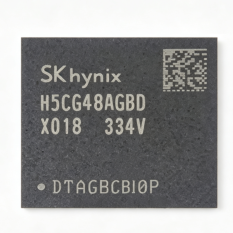
H5CG48AGBDX018N - DDR5 16Gb 5600Mbps DRAM | SK hynix
The SK hynix H5CG48AGBDX018N is a 16Gb DDR5 SDRAM memory IC organized as 2Gx8, operating at data rates up to 5600 Mbps from a 1.1V supply, housed in an 82-ball FCBGA (JEDEC DDR5 78/82-ball) surface-mount package. DDR5 SDRAM is the fifth generation of Double Data Rate synchronous dynamic random-access memory, a class of volatile memory ICs within the broader memory and power-management hierarchy of modern computing systems. Compared with DDR4, DDR5 doubles the bank count, moves the power management IC (PMIC) onto the memory module, reduces the per-channel word length to 16 bits, and lowers the operating voltage from 1.2V to 1.1V, which together raise bandwidth and improve power efficiency for servers, workstations, and AI computing platforms. Key features of the H5CG48AGBDX018N include the 16Gb (2G x 8) single-die density, DDR5-5600 speed grade with an 8-bit data bus width, and a nominal 1.1V core supply that reduces dynamic power versus DDR4-class parts. The x8 organization simplifies memory controller configuration for embedded and module designs, and the device is rated for operation across a -40C to +85C temperature range per distributor data, supporting industrial environments in addition to consumer and computing applications. Technically, the part is manufactured on SK hynix advanced DRAM process technology (the A-die generation per cross-reference sources) and follows the JEDEC DDR5 SDRAM standard interface, including on-die ECC support, decision-feedback equalization (DFE) on the DQ receivers, and an I3C-based sideband bus for host control, all standard characteristics of the DDR5 generation. These features maintain signal integrity at 5600 Mbps pin speeds on conventional PCB stackups. Typical applications include server main memory, AI and high-performance computing modules, industrial controllers requiring firmware boot and embedded logging memory, computing modules and consumer electronics, and replacement sourcing for DDR5-based BOM lines. A key design consideration: DDR5 does not run from a fixed 1.1V rail in module designs - the on-module PMIC regulates the rail, so discrete (solder-down) designs must provide a dedicated 1.1V supply with proper decoupling and follow JEDEC fly-by routing for CA and DQ signals. This page synthesizes distributor pricing, drop-in alternatives, design notes, and lifecycle context not consolidated in the manufacturer datasheet.
H5CG48MEBDX014N - DDR5 16Gb 4800Mbps SDRAM | SK Hynix
The SK Hynix H5CG48MEBDX014N is a 16Gb (2G x 8) DDR5 SDRAM DRAM component operating at 4800 Mbps data rate, fabricated on SK Hynix M-die process and housed in an 82-ball FBGA package measuring 11 x 10 mm. DDR5 SDRAM (double data rate fifth generation synchronous dynamic random-access memory) is the current generation of main-memory DRAM used in servers, workstations, desktop PCs, and high-performance embedded systems. In the memory hierarchy, DRAM sits below CPU caches and above storage, providing the primary working memory for processors. DDR5 doubles the bank groups and banks per device versus DDR4, splits the power supply so VDDQ is separate from VDD, and moves the power management onto the module via PMIC, delivering higher bandwidth and better power efficiency than DDR4 SDRAM. Key features of the H5CG48MEBDX014N include 16 Gbit density organized as 2G x 8, a 4800 Mbps (PC5-class) data transfer rate, a low 1.1 V nominal core operating voltage, and an operating temperature range of 0C to +95C as listed by distributors. The part carries 12 row address bits and 9 column address bits, per Octopart documentation, giving the addressing structure used in modern DDR5 memory controllers. The x8 organization simplifies ECC-based server module designs where multiple x8 devices provide chipkill-class error coverage. The M-die generation uses SK Hynix advanced DRAM process technology to achieve the 4800 Mbps speed grade at JEDEC-standard DDR5 voltage levels. On-die termination, decision-feedback equalization, and same-bank refresh enhancements characteristic of DDR5 enable reliable signaling at these data rates on standard PCB stackups. Typical applications include server and datacenter DIMMs, desktop and workstation UDIMMs, AI accelerators and high-performance computing boards, industrial systems requiring high memory bandwidth, and embedded compute designs. Design consideration: DDR5 routing requires careful length matching of DQ/CA buses and proper VDDQ decoupling; always validate speed-bin settings and refresh configuration in the memory controller against the manufacturer datasheet. This page synthesizes distributor pricing, cross-referenced drop-in alternatives including SK Hynix A-die and Samsung equivalents, and supply-chain availability data not found in the manufacturer datasheet.
H5CG48MEBDX018 - DDR5 16Gb 4800Mbps DRAM | SK Hynix
The SK hynix H5CG48MEBDX018 is a 16Gb DDR5 SDRAM DRAM component organized as 2G x8, rated for DDR5-4800 (4800 Mbps data rate), operating from a 1.1V supply in an FCBGA (BGA-78/82-ball) surface-mount package, suited for next-generation compute platforms. DDR5 SDRAM is the fifth generation of Double Data Rate synchronous dynamic random access memory, the dominant main-memory technology in servers, workstations, desktops, and embedded compute modules. Within the memory hierarchy, DDR5 sits above LPDDR (low-power variants for mobile) and GDDR (graphics variants), and is the standard JEDEC-defined DRAM interface for high-bandwidth compute systems. Key features include the 16 Gbit density per die (2G x16 x 8 organization equivalent, 2G x8 bus), a 4800 Mbps data rate, and the DDR5 on-die ECC (ODECC) architecture that improves reliability versus DDR4. The 1.1V core supply reduces per-bit power consumption compared with the 1.2V DDR4 generation, while the on-PDIMM power management architecture moves PMIC functions off the DRAM die, improving signal integrity and efficiency. Technically, the H5CG48MEBDX018 belongs to SK hynix DDR5 SDRAM family; part numbering indicates an M-die generation at the 4800 class speed grade with an 8-bit bus width. The DDR5 interface uses two independent 32-bit sub-channels per module, improving effective concurrency versus the single 64-bit channel of DDR4. Typical applications include PC and workstation DIMMs/Ultra-DIMMs, embedded compute and edge-AI modules, networking equipment line cards, and industrial systems requiring high-density main memory. A key design consideration: DDR5 routing requires careful length matching of DQ/CA and DQS byte lanes, and on-die ECC must be enabled at the memory controller level. This page synthesizes distributor pricing, drop-in alternatives within the SK hynix DDR5 family, and practical sourcing guidance not found in the manufacturer datasheet.
H5CG48MEBDX018N - DDR5 16Gb SDRAM FCBGA | SK Hynix
The SK Hynix H5CG48MEBDX018N is a 16Gb (2G x 8) DDR5 SDRAM DRAM IC manufactured on SK Hynix M-die process technology, supplied in a 78-ball FCBGA surface-mount package for computing and embedded memory subsystems. DDR5 SDRAM is the fifth generation of Double Data Rate synchronous dynamic random-access memory, the dominant main-memory technology hierarchy that runs from DRAM cell arrays up through memory ICs to full memory modules (DIMMs) and, more broadly, semiconductor storage subsystems. Compared with DDR4, DDR5 doubles the bank groups, moves the power management IC (PMIC) onto the module, and lowers the per-pin operating voltage to 1.1V, enabling higher data rates with improved power efficiency. Key features of this device include a 16Gb density organized as 2G x 8, an 8-bit data bus width, a nominal 1.1V supply, and family data rates spanning 4800 Mbps to 5600 Mbps. DDR5-specific features such as on-die ECC (ODECC), decision-feedback equalization (DFE), and same-bank refresh improve effective reliability and bandwidth utilization in high-density configurations. Technically, the H5CG48MEBDX018N belongs to SK Hynix M-die DDR5 generation; the M-die variants (H5CG48MEBDX014N at 4800 Mbps) are widely documented as drop-in replacements for earlier A-die parts such as the H5CG48AGBDX018N at DDR5-5600, per published cross-reference guidance. Package ballout and command/address pin assignment follow the JEDEC DDR5 x8 component convention, allowing single-sourcing BOM flexibility within the family. Typical applications include PC and workstation main memory, server and data center RDIMM/DIMM modules, embedded computing modules, industrial controllers, and network appliances requiring high-bandwidth main memory. Design consideration: verify the exact data-rate bin and speed-grade suffix of your BOM line against the system memory controller DDR5 training range, since 4800 Mbps and 5600 Mbps variants share the package footprint but differ in timing parameters. This page synthesizes distributor inventory, family cross-references, and practical design notes not found in the manufacturer datasheet.
H5TC4G63AFR-G7A - 4Gb DDR3L SDRAM 1.35V | SK Hynix
The H5TC4G63AFR-G7A is a 4Gb DDR3L SDRAM from SK Hynix, organized as 256M x 16 bits, operating at 1.35V for low power consumption. It is part of the H5TC4G63AFR family, which includes H5TC4G43AFR and H5TC4G83AFR variants, all designed for main memory applications requiring high density, high bandwidth, and low power. The device is lead-free and halogen-free, RoHS compliant, and comes in a 96-ball FBGA package. DDR3L (Double Data Rate 3 Low Voltage) SDRAM is a type of synchronous dynamic random-access memory that operates at 1.35V, reducing power consumption by about 20% compared to standard DDR3 (1.5V). It is part of the DDR3 SDRAM family, which uses double data rate signaling to transfer data on both edges of the clock, achieving high bandwidth. DDR3L is commonly used in mobile devices, embedded systems, and servers where power efficiency is critical. Key features include a 4Gb density, 256M x 16 organization, 1.35V power supply, and a data rate of 1600 Mbps (PC3-12800) as indicated by the -G7A speed grade. The device supports on-die termination (ODT), programmable CAS latency, and burst lengths of 8 and 4. It operates over a temperature range of 0°C to 95°C (case temperature) and is available in a 96-ball FBGA package. The H5TC4G63AFR-G7A uses a CMOS process technology, ensuring high performance and low power. It features auto refresh and self refresh modes, with a refresh period of 7.8us at 85°C. The device includes a mode register for programming various operating parameters, such as CAS latency and burst length. The 96-ball FBGA package provides excellent thermal and electrical performance, making it suitable for space-constrained designs. Typical applications include laptops, ultrabooks, embedded systems, networking equipment, and industrial computing. The low voltage operation makes it ideal for battery-powered devices where power consumption is a concern. The high bandwidth supports memory-intensive applications such as video processing and gaming. When designing with this device, ensure proper decoupling capacitors are placed near the power pins to minimize noise. The VDD and VDDQ should be supplied with 1.35V, and the reference voltage VREF should be set to 0.675V. Follow the PCB layout guidelines in the datasheet to ensure signal integrity at high speeds.
H5TC4G63AFR-H9A - 4Gb DDR3L SDRAM 256Mx16 | SK hynix
The H5TC4G63AFR-H9A is a 4Gb DDR3L SDRAM organized as 256M x 16, operating at 1.35V, in a 96-ball FBGA package. It is part of SK hynix's DDR3L family, designed for low-power main memory applications requiring high density and bandwidth. The device supports data rates up to 1866 Mbps (PC3-14900) with a CAS latency of 13, and is lead-free and halogen-free, RoHS compliant. DDR3L (Double Data Rate 3 Low Voltage) SDRAM is a type of synchronous dynamic random-access memory that operates at 1.35V, reducing power consumption by about 15% compared to standard 1.5V DDR3. It is part of the DDR3 memory family, which uses double data rate signaling to transfer data on both edges of the clock, and is widely used in laptops, embedded systems, and networking equipment where power efficiency is critical. Key features include a 4Gb density, 16-bit I/O width, 1.35V core and I/O supply, and a 96-ball FBGA package. The device offers programmable CAS latency, burst lengths of 8 and 4, and on-die termination (ODT) for signal integrity. It supports auto-refresh and self-refresh modes, and includes a temperature-compensated self-refresh (TCSR) feature for low-power standby. Technically, the H5TC4G63AFR-H9A uses a 30nm-class process technology, achieving high density with low power. The -H9A speed grade indicates a tCK of 1.07ns (DDR3L-1866) and CL13. The device features a 16n prefetch architecture, enabling high bandwidth. It also includes programmable impedance calibration (ZQ calibration) for improved signal quality. Typical applications include main memory for ultra-thin laptops, embedded computing, networking routers, and industrial PCs. Its low voltage and high density make it ideal for space-constrained designs where power and performance are balanced. When designing with this device, ensure proper decoupling with 0.1uF and 1uF capacitors near the power pins, and follow the PCB layout guidelines for DDR3 routing to maintain signal integrity at 1866 Mbps.
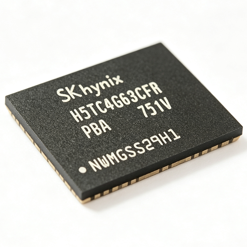
H5TC4G63AFR-PBA - 4Gb DDR3L SDRAM 256Mx16 | SK hynix
The H5TC4G63AFR-PBA is a 4Gb DDR3L SDRAM organized as 256M x 16, manufactured by SK hynix. It operates at a low voltage of 1.35V, reducing power consumption by approximately 15% compared to standard DDR3 (1.5V). The device is housed in a 96-ball FBGA package, offering a compact footprint suitable for space-constrained applications. With a data rate of up to 1866 Mbps (PC3L-14900), it delivers high bandwidth for demanding computing tasks. DDR3L SDRAM is a type of dynamic random-access memory that uses double data rate architecture, transferring data on both edges of the clock signal. It is part of the DDR3 family, which succeeded DDR2 and was widely adopted in PCs, servers, and embedded systems. DDR3L specifically operates at 1.35V, making it ideal for power-sensitive applications such as laptops, networking equipment, and industrial computing. Key features include a 16-bit I/O interface, 8 internal banks, and support for burst lengths of 8 and 4 (with burst chop). The device includes on-die termination (ODT), ZQ calibration, and write leveling for improved signal integrity. It also supports auto self-refresh and partial array self-refresh for power savings. The operating temperature range is 0°C to +95°C (Tcase), suitable for commercial and industrial environments. Technically, the H5TC4G63AFR-PBA uses a CMOS process and features programmable CAS latency (CL) of 11, 12, and 13, with corresponding tRCD and tRP values. The device supports DLL (Delay-Locked Loop) for precise timing and includes a mode register for configuration. The 96-ball FBGA package has a ball pitch of 0.8mm, enabling high-density PCB layouts. Typical applications include DDR3L memory modules for laptops, embedded systems, networking routers, and industrial PCs. Its low voltage and high density make it suitable for designs requiring energy efficiency and compactness. The device is also used in set-top boxes and automotive infotainment systems. When designing with this component, ensure proper decoupling capacitors near the power pins and follow the layout guidelines in the datasheet to maintain signal integrity at high speeds. The VDD and VDDQ should be supplied with 1.35V, and the reference voltage (VREF) must be generated accurately.
H5TC4G63AFR-PBI - 4Gb DDR3L SDRAM 256Mx16 | SK Hynix
The SK Hynix H5TC4G63AFR-PBI is a 4Gb DDR3L SDRAM organized as 256Mx16, operating at 1.35V with a data rate of DDR3-1600 (PC3L-12800). It comes in a 96-ball FBGA package (TFBGA, BGA96, 9x16, 32) and is designed for industrial temperature range (-40°C to +95°C). This memory device is widely used in networking, embedded computing, and industrial applications where low power and high density are required. DDR3L (Double Data Rate 3 Low Voltage) SDRAM is a type of synchronous dynamic random-access memory that operates at a lower voltage (1.35V) compared to standard DDR3 (1.5V), reducing power consumption by up to 20% while maintaining similar performance. It is part of the DDR3 memory family, which uses double data rate signaling to transfer data on both edges of the clock, and is commonly used in servers, routers, and industrial PCs. DDR3L is backward compatible with DDR3 slots in many designs, making it a versatile choice for memory upgrades. Key features include a 16-bit I/O width, 8 internal banks, and a burst length of 8 (BL8) with on-die termination (ODT) and programmable CAS latency. The device supports auto-refresh and self-refresh modes, with a typical refresh period of 7.8us at 85°C. The industrial temperature grade ensures reliable operation in harsh environments, and the 96-ball FBGA package provides a compact footprint for space-constrained designs. The H5TC4G63AFR-PBI uses a CMOS process technology and features a pseudo-open-drain output driver with adjustable impedance. It includes a DLL (Delay-Locked Loop) for precise timing alignment and supports write leveling for improved signal integrity. The memory operates from a single 1.35V supply, with an on-chip voltage regulator for the core, reducing external component count. Typical applications include network routers and switches, industrial automation controllers, embedded computing modules, and test and measurement equipment. Its low voltage and high density make it ideal for power-sensitive systems that require large memory capacity. When designing with this device, ensure proper decoupling capacitors are placed near the VDD and VDDQ pins, and follow the PCB layout guidelines in the datasheet to minimize signal integrity issues. The device requires a stable 1.35V supply and a clean clock signal for reliable operation.
H5TC4G63AFR-PBJ - 4Gb DDR3L SDRAM 256Mx16 | SK Hynix
The SK Hynix H5TC4G63AFR-PBJ is a 4Gb DDR3L SDRAM organized as 256M x 16, operating at 1.35V to reduce power consumption while delivering high bandwidth for main memory applications. It comes in a 96-ball TFBGA package with industrial temperature grade, making it suitable for embedded systems, networking equipment, and industrial computing. DDR3L (Double Data Rate 3 Low Voltage) is a type of synchronous dynamic random-access memory (SDRAM) that operates at 1.35V, offering a 15% power reduction compared to standard DDR3 at 1.5V. It is part of the DDR3 family, which uses double data rate signaling to transfer data on both edges of the clock, achieving high bandwidth. DDR3L is widely used in laptops, servers, and embedded systems where power efficiency is critical. Key features include a 256M x 16 organization, 96-ball TFBGA package, industrial temperature grade (-40°C to +95°C), and support for 8192 refresh cycles. The device supports auto self-refresh, data mask, auto precharge, asynchronous reset, dynamic on-chip termination (DTC), ZQ calibration, and write leveling, ensuring reliable operation in demanding environments. The H5TC4G63AFR-PBJ uses a CMOS process and features a rectangular package shape. It is designed for high-density, high-bandwidth, and low-power applications. The industrial temperature grade allows operation in harsh conditions, making it ideal for automotive, industrial, and networking applications. Typical applications include main memory for embedded processors, networking routers and switches, industrial PCs, and test equipment. The low voltage and high bandwidth make it suitable for power-sensitive designs. When designing with this device, ensure proper decoupling and signal integrity practices are followed. The ZQ calibration pin requires a 240-ohm resistor to ground for optimal signal quality.
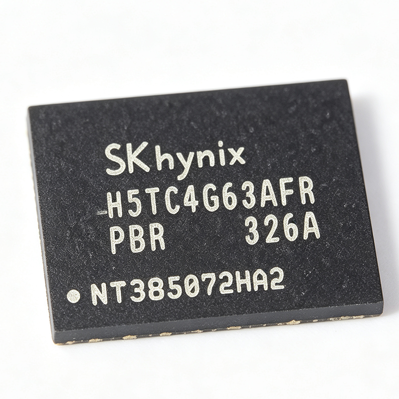
H5TC4G63AFR-PBR - 4Gb DDR3L SDRAM 256Mx16 | SK Hynix
The H5TC4G63AFR-PBR is a 4Gb DDR3L SDRAM (Double Data Rate 3 Low Voltage) organized as 256M x 16, manufactured by SK Hynix. It operates at a supply voltage of 1.35V (with 1.5V compatibility) and is housed in a 96-ball FBGA package (PBGA96). This memory device is designed for high-speed data transfer with a data rate of 1600 Mbps (PC3L-12800), featuring a CAS latency of 11 and a tRCD/tRP of 11. The device supports on-die termination (ODT), programmable CAS latency, and burst lengths of 8 and 4 (with burst chop). It is compliant with the JEDEC DDR3L standard, ensuring interoperability with a wide range of controllers. DDR3L SDRAM is a type of synchronous dynamic random-access memory that transfers data on both edges of the clock signal, effectively doubling the data rate. It is a low-voltage variant of DDR3, operating at 1.35V instead of 1.5V, which reduces power consumption by approximately 15-20% compared to standard DDR3. DDR3L is part of the DDR SDRAM family, which includes DDR, DDR2, DDR3, and DDR4, and is widely used in computing, networking, and embedded systems. The low-voltage operation makes it ideal for power-sensitive applications such as laptops, servers, and industrial electronics. Key features of the H5TC4G63AFR-PBR include a 16-bit I/O interface, 8 internal banks, and a burst length of 8 (BL8) with burst chop (BC4). It supports auto refresh and self refresh modes, with a refresh interval of 7.8us at 85C and 3.9us at 95C. The device has a programmable output driver impedance and on-die termination for improved signal integrity. It also features a temperature-compensated self-refresh (TCSR) and a partial array self-refresh (PASR) for power savings. The package is a 96-ball FBGA with a 0.8mm ball pitch, measuring 13.5mm x 9.0mm, and is RoHS compliant. Technically, the H5TC4G63AFR-PBR uses a CMOS process and supports a clock frequency up to 800 MHz (DDR3L-1600). It has a tCK of 1.25ns and a tRCD of 13.125ns. The device includes a mode register set (MRS) for configuration and supports write leveling and read leveling for improved signal integrity. The I/O interface is SSTL-15 compatible, and the device supports a data strobe (DQS) differential pair. The memory is organized into 8 banks of 32M x 16, providing a total capacity of 4Gb. The device is designed for high-reliability applications and is available in a lead-free, halogen-free package. Typical applications for the H5TC4G63AFR-PBR include embedded systems, networking equipment (routers, switches), industrial PCs, and consumer electronics such as set-top boxes and smart TVs. Its low-voltage operation and high density make it suitable for memory-intensive applications where power efficiency is critical. The device is also used in automotive infotainment systems and medical devices that require reliable, high-speed memory. When designing with this device, ensure proper decoupling capacitors (0.1uF and 1uF) are placed near the VDD and VDDQ pins to minimize noise. The VREFCA and VREFDQ should be bypassed with 0.1uF capacitors. The device requires a stable 1.35V supply and a separate 1.35V VDDQ supply. For optimal signal integrity, route the DQ, DQS, and address lines with matched trace lengths and controlled impedance (typically 50 ohms single-ended, 100 ohms differential).
H5TC4G63CFR-H9A - 4Gb DDR3L SDRAM 96-FBGA | SK hynix
The H5TC4G63CFR-H9A is a 4Gb DDR3L SDRAM manufactured by SK hynix, organized as 256M x 16 bits. It operates at a low voltage of 1.35V (VDD=VDDQ=1.35V + 0.100 / - 0.067V), enabling power-efficient main memory solutions. The device is housed in a 96-ball TFBGA package, providing a compact footprint for space-constrained designs. It is lead-free and halogen-free, fully RoHS compliant, and supports a temperature range suitable for commercial and industrial applications. DDR3L SDRAM is a type of synchronous dynamic random-access memory that operates at a lower voltage (1.35V) compared to standard DDR3 (1.5V), reducing power consumption by up to 20% while maintaining backward compatibility with DDR3 environments. It is part of the DDR3 memory family, which uses double data rate architecture to transfer data on both edges of the clock, achieving high bandwidth. DDR3L is widely used in laptops, embedded systems, and networking equipment where energy efficiency is critical. Key features include fully differential clock inputs (CK, CK), differential data strobe (DQS, DQS), and an on-chip DLL that aligns DQ, DQS, and DQS transitions with CK transitions. The DM (data mask) function masks write data at both rising and falling edges, ensuring data integrity. The device supports burst lengths of 8 and 4 (with burst chop), and features programmable CAS latency and additive latency for flexible timing. The H5TC4G63CFR-H9A is designed for high-bandwidth, low-power main memory applications. Its 4Gb density and x16 organization make it ideal for applications requiring large memory capacity with a moderate bus width. The 96-ball TFBGA package offers excellent thermal and electrical performance, with a ball pitch of 0.8mm, facilitating high-density PCB layouts. Typical applications include laptops and ultrabooks, embedded computing, networking switches and routers, and industrial automation systems. The low operating voltage and high bandwidth make it suitable for battery-powered devices and energy-conscious designs. When designing with this component, ensure proper decoupling capacitors are placed near the VDD and VDDQ pins to minimize noise. The device requires a stable 1.35V supply and careful signal integrity management for the high-speed data bus. Refer to the datasheet for detailed timing parameters and PCB layout guidelines.
H5TC4G63CFR-H9I - 4Gb DDR3L SDRAM 256Mx16 | SK hynix
The H5TC4G63CFR-H9I is a 4Gb DDR3L SDRAM from SK hynix, organized as 256M x 16 bits. It operates at a low voltage of 1.35V, reducing power consumption by about 15% compared to standard DDR3 (1.5V). The device is housed in a 96-ball TFBGA package and is designed for industrial temperature range (-40°C to +95°C). It is lead-free and halogen-free, compliant with RoHS. DDR3L SDRAM is a type of dynamic random-access memory that uses double data rate architecture, transferring data on both edges of the clock. It is a key component in computing systems, providing high bandwidth and low power operation for main memory applications. The H5TC4G63CFR-H9I is part of the DDR3L family, which is widely used in servers, networking equipment, and embedded systems. Key features include a 4Gb density, 16-bit data bus, and support for data rates up to 1866 Mbps (PC3-14900). The device operates from a 1.35V supply, with an I/O voltage of 1.35V. It features programmable CAS latency, burst lengths of 8 and 4, and on-die termination (ODT) for improved signal integrity. The industrial temperature grade ensures reliable operation in harsh environments. The H5TC4G63CFR-H9I uses a high-performance CMOS process and advanced circuit design to achieve fast access times and low power consumption. It includes auto-refresh and self-refresh modes to minimize power in standby. The TFBGA package provides excellent thermal and electrical performance, making it suitable for space-constrained designs. Typical applications include main memory for industrial PCs, networking routers, and embedded computing modules. Its low voltage and industrial temperature range make it ideal for applications requiring reliability and energy efficiency. When designing with this device, ensure proper decoupling and signal integrity practices are followed. The DDR3L interface requires careful PCB layout to maintain signal quality at high speeds.
H5TC4G63CFR-H9J - 4Gb DDR3L SDRAM 96-Ball TFBGA | SK Hynix
The H5TC4G63CFR-H9J is a 4Gb DDR3L SDRAM from SK Hynix, organized as 256M x 16, operating at a nominal supply voltage of 1.35V (VDD=VDDQ=1.35V +0.100/-0.067V). It is housed in a 96-ball TFBGA (Thin Fine-Pitch Ball Grid Array) package with a rectangular body, designed for high-density main memory applications requiring low power and high bandwidth. The device is lead-free and halogen-free, compliant with RoHS regulations, and supports industrial temperature grades. DDR3L (Double Data Rate 3 Low Voltage) SDRAM is a type of synchronous dynamic random-access memory that operates at a lower voltage (1.35V) compared to standard DDR3 (1.5V), reducing power consumption by approximately 20-30% while maintaining similar performance. It is part of the DDR3 memory family, which uses double data rate signaling to transfer data on both rising and falling edges of the clock, and is widely used in servers, networking equipment, and embedded systems where power efficiency is critical. Key features include fully differential clock inputs (CK, CK) for improved signal integrity, differential data strobes (DQS, DQS) for precise data capture, and an on-chip DLL that aligns DQ, DQS, and DQS transitions with the CK transition. The DM (Data Mask) function masks write data on both rising and falling edges, enabling byte-level write operations. The device supports industrial temperature range, making it suitable for harsh environments. Technically, the H5TC4G63CFR-H9J utilizes a CMOS process and features a 4-bit prefetch architecture typical of DDR3, achieving data rates up to 1866 Mbps (PC3-14900) at the -H9 speed grade. The 96-ball TFBGA package provides excellent thermal and electrical performance, with a compact footprint for space-constrained designs. The device is designed for high reliability and low power operation, with support for on-die termination (ODT) and programmable CAS latency. Typical applications include main memory for industrial PCs, networking routers and switches, embedded computing modules, and high-performance storage systems. The low voltage and high density make it ideal for power-sensitive applications where battery life or thermal management is a concern. When designing with this device, ensure proper decoupling of the VDD and VDDQ supplies with 0.1uF and 1uF capacitors placed close to the balls. Follow the PCB layout guidelines in the datasheet for signal integrity, especially for the differential clock and data strobe pairs.
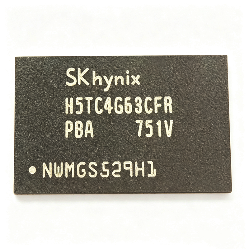
H5TC4G63CFR-PBA - 4Gb DDR3L SDRAM 256Mx16 | SK Hynix
The H5TC4G63CFR-PBA is a 4Gb DDR3L SDRAM organized as 256M x 16, manufactured by SK Hynix. It operates at VDD=VDDQ=1.35V with a tolerance of +0.100/-0.067V, enabling low-power operation for mobile and embedded systems. The device is housed in a 96-ball FBGA package (PBGA96) and is lead-free and halogen-free, fully RoHS compliant. DDR3L (Double Data Rate 3 Low Voltage) SDRAM is a type of synchronous dynamic random-access memory that operates at 1.35V, reducing power consumption by about 20% compared to standard DDR3 (1.5V). It is part of the DDR3 memory family, which uses double data rate signaling to transfer data on both edges of the clock, and is widely used in computing, networking, and industrial applications where power efficiency is critical. Key features include fully differential clock inputs (CK, CK) for improved signal integrity, differential data strobe (DQS, DQS) for precise data capture, and an on-chip DLL that aligns DQ, DQS, and DQS transitions with CK. The DM (data mask) function masks write data on both rising and falling edges, and the device supports auto precharge, auto self-refresh, and dynamic on-chip termination (ODT) for signal quality. The H5TC4G63CFR-PBA uses a CMOS process and includes ZQ calibration for output driver and ODT impedance matching, write leveling for command/address timing, and asynchronous reset for initialization. These features ensure reliable high-speed operation and simplify system design. Typical applications include DDR3L memory modules for laptops, embedded systems, networking equipment (routers, switches), and industrial PCs. Its low voltage and high density make it ideal for power-sensitive designs. When designing with this device, ensure proper decoupling and follow the PCB layout guidelines in the datasheet to maintain signal integrity at high frequencies. The device requires a stable 1.35V supply and careful termination of the differential clock and strobe lines.
H5TC4G63CFR-PBL - 4Gb DDR3L SDRAM 256Mx16 | SK hynix
The H5TC4G63CFR-PBL is a 4Gb DDR3L SDRAM (Double Data Rate 3 Low Voltage) memory chip from SK hynix, organized as 256M x 16 bits. It operates at a low voltage of 1.35V, making it ideal for power-sensitive applications such as mobile devices, embedded systems, and networking equipment. The device is available in a 96-ball FBGA package (TFBGA) and is lead-free and halogen-free, complying with RoHS standards. DDR3L SDRAM is a type of synchronous dynamic random-access memory that transfers data on both edges of the clock signal, doubling the data rate compared to single data rate SDRAM. The 'L' denotes low voltage operation at 1.35V, reducing power consumption by about 15% compared to standard DDR3 at 1.5V. This makes DDR3L a preferred choice for battery-powered and thermally constrained designs. Key features of the H5TC4G63CFR-PBL include a data rate of 1600 Mbps (PC3L-12800), a burst length of 8, and support for on-die termination (ODT) and posted CAS. The device also features auto refresh and self refresh modes, with a typical refresh period of 7.8 us at 85C. The 96-ball FBGA package provides a compact footprint suitable for high-density PCB layouts. The H5TC4G63CFR-PBL uses a high-performance CMOS process technology, ensuring fast access times and low power consumption. The memory array is organized into 8 banks, each with 32K rows, providing efficient row activation and precharge operations. The device supports a programmable CAS latency of 11, 12, and 13, allowing flexibility in system timing. Typical applications include main memory for laptops, ultrabooks, and embedded systems, as well as networking equipment such as routers and switches, and industrial automation controllers. The low voltage and high bandwidth make it suitable for applications requiring high memory density and low power. When designing with this device, ensure proper decoupling capacitors are placed near the VDD and VDDQ pins to minimize power supply noise. Also, follow the JEDEC DDR3L layout guidelines for signal integrity, especially for high-speed data lines.
H5TC4G63CFR-xxI - 4Gb DDR3L SDRAM | SK Hynix
The H5TC4G63CFR-xxI is a 4Gb DDR3L SDRAM manufactured by SK Hynix, designed for main memory applications requiring high density, high bandwidth, and low power operation at 1.35V. It operates with VDD=VDDQ=1.35V +0.100/-0.067V, features fully differential clock inputs (CK, CK), differential data strobes (DQS, DQS), and an on-chip DLL to align DQ, DQS, and DQS transitions with CK. The device is lead-free and halogen-free, RoHS compliant, and comes in a 78-ball FBGA package. DDR3L (Double Data Rate 3 Low Voltage) SDRAM is a type of synchronous dynamic random-access memory that achieves high data transfer rates by transferring data on both edges of the clock signal. It operates at a lower voltage (1.35V) compared to standard DDR3 (1.5V), reducing power consumption by about 20% while maintaining similar performance. DDR3L is part of the DDR3 memory family, which is widely used in computing, networking, and embedded systems. Key features include a 4Gb density organized as 512M x 8, a data rate of [DATA_NEEDED: speed grade] (e.g., 1600 Mbps), and support for 1.35V operation. The device uses an 8n-prefetch architecture, which enables high bandwidth by fetching 8 data words per clock cycle. It also supports on-die termination (ODT), programmable CAS latency, and burst lengths of 8 and 4 (with burst chop). The H5TC4G63CFR-xxI is fabricated using advanced DRAM process technology, ensuring high reliability and low power consumption. The on-chip DLL synchronizes the output data with the clock, reducing skew and improving signal integrity. The device includes auto-refresh and self-refresh modes for low-power standby, and it supports temperature-compensated self-refresh (TCSR) to optimize refresh rate based on operating temperature. Typical applications include servers, networking equipment, industrial computing, and embedded systems where high memory density and low power are critical. The 1.35V operation makes it ideal for power-sensitive designs, such as laptops, portable devices, and energy-efficient data centers. When designing with this device, ensure proper decoupling of VDD and VDDQ with 0.1uF capacitors placed close to the pins. Follow the DDR3L layout guidelines for signal integrity, including matched trace lengths for DQ, DQS, and address/command signals. The device requires a stable 1.35V supply and a clean reference voltage (VREF) for optimal operation.
H5TC4G63CFR-xxJ - 4Gb DDR3L SDRAM 256Mx16 | SK Hynix
The H5TC4G63CFR-xxJ is a 4Gb DDR3L SDRAM manufactured by SK Hynix, organized as 256M x 16. It operates at a low supply voltage of VDD = VDDQ = 1.35V, making it ideal for power-sensitive applications such as mobile devices, embedded systems, and networking equipment. The device features fully differential clock inputs (CK, CK#), differential data strobes (DQS, DQS#), and an on-chip DLL that aligns DQ, DQS, and DQS# transitions with the CK transition. It is lead-free and halogen-free, compliant with RoHS standards. DDR3L SDRAM (Double Data Rate 3 Low Voltage) is a type of synchronous dynamic random-access memory that transfers data on both rising and falling edges of the clock signal, effectively doubling the data rate. DDR3L operates at 1.35V, reducing power consumption by about 20% compared to standard DDR3 (1.5V), while maintaining compatibility with DDR3 signaling levels. It is part of the memory hierarchy in computing systems, serving as main memory for processors, and is widely used in laptops, servers, and embedded applications. Key features include a 4Gb density, 16-bit I/O width, and support for various speed grades (e.g., -xxJ indicates a specific speed grade, likely 1600 Mbps or 1866 Mbps). The device uses a 96-ball FBGA package, which is standard for DDR3L SDRAM, ensuring compatibility with existing PCB designs. The operating temperature range is from 0°C to 95°C (case temperature), and it supports auto-refresh and self-refresh modes for power saving. Technically, the H5TC4G63CFR-xxJ employs an 8n-prefetch architecture, which allows high-speed data transfer by fetching 8 data bits per clock cycle per I/O. It includes programmable CAS latency, burst length (8 and 4 with burst chop), and on-die termination (ODT) for signal integrity. The device also supports write leveling and read leveling for improved timing margins in high-speed systems. Typical applications include main memory for laptops, ultrabooks, and embedded systems, as well as networking equipment like routers and switches, and industrial computing platforms. Its low voltage and high density make it suitable for power-constrained designs that require large memory capacity. When designing with this component, ensure proper decoupling capacitors near the VDD and VDDQ pins, and follow the DDR3L layout guidelines for signal integrity, including impedance matching and length matching for data and address lines. The device requires a stable 1.35V supply and a reference voltage (VREF) for the command/address bus.