Memory ICs
Subcategories
Products (487)
H5AN8G6NAFR-UHC - 8Gb DDR4 SDRAM 2400MT/s | SK Hynix
The SK Hynix H5AN8G6NAFR-UHC is an 8Gbit CMOS DDR4 SDRAM organized as 512M x 16, operating at 1.2V and 2400MT/s data rate, housed in a 96-ball FBGA (TFBGA) surface-mount package. It is ideally suited for main-memory applications requiring large memory density and high bandwidth. DDR4 SDRAM (Double Data Rate 4 Synchronous Dynamic Random Access Memory) is the fourth generation of the DDR memory hierarchy, succeeding DDR3. A DRAM stores each bit in a capacitor-based cell and requires periodic refresh; DDR4 doubles bank-group parallelism versus DDR3, lowers operating voltage to 1.2V, and transfers data on both rising and falling clock edges referenced to a differential clock (CK_t/CK_c). Key features of this device include fully synchronous operation referenced to both edges of the differential clock, an asynchronous reset function, auto self-refresh and auto precharge, a data mask (DM) function for byte-wise write masking, dynamic on-chip termination (ODT), ZQ calibration, CRC function, and write leveling. Per LCSC product data, the device operates from 0C to +85C. Architecturally, all address and control input signals are sampled on the crossing of the positive edge of CK_t and negative edge of CK_c, while data is captured relative to data strobes (DQS_t/DQS_c) supporting source-synchronous timing. The 512M x 16 organization provides a 16-bit data width suited to embedded CPUs, industrial controllers, and memory-down designs that avoid DIMM connectors. Typical applications include main memory for embedded and industrial systems, networking equipment, set-top boxes, and high-bandwidth buffer memory in storage and imaging systems where large density and high bandwidth are required. A key design consideration is DDR4 signal integrity: routing length matching of DQ to DQS, ZQ resistor placement, and proper VDDQ termination planning are essential; the dynamic ODT and write-leveling features of this part help manage fly-by command routing on multi-device buses. This page synthesizes distributor pricing, drop-in alternatives, and practical design notes not found in the manufacturer datasheet.
H5AN8G6NAFR-UHC - 8Gb DDR4 SDRAM 512Mx16 | SK hynix
The H5AN8G6NAFR-UHC is an 8Gb CMOS Double Data Rate IV (DDR4) Synchronous DRAM from SK hynix, organized as 512M x 16 bits. It operates from a 1.2V supply and is available in a 96-ball FBGA package. This device is designed for main memory applications requiring high density and bandwidth, supporting data rates up to 2400 MT/s (PC4-19200). DDR4 SDRAM is a type of synchronous dynamic random-access memory that transfers data on both rising and falling edges of the clock, doubling the data rate compared to single-data-rate SDRAM. It is the fourth generation of DDR memory, offering higher speed, lower voltage (1.2V vs 1.5V for DDR3), and improved power efficiency. DDR4 is widely used in servers, desktops, laptops, and embedded systems where high memory bandwidth and capacity are critical. Key features include fully synchronous operation referenced to both clock edges, programmable CAS latency, burst lengths of 8 and 4 (with burst chop), on-die termination (ODT) for signal integrity, and ZQ calibration for improved timing. The device supports auto self-refresh, auto precharge, data mask, write leveling, and CRC error detection, enhancing reliability in high-speed systems. It is lead-free and halogen-free, compliant with RoHS. Architecturally, the H5AN8G6NAFR-UHC uses a 20nm-class process technology, enabling high density with low power consumption. The 512M x 16 organization is ideal for memory modules and embedded applications requiring a 16-bit data bus. The FBGA-96 package provides excellent thermal and electrical performance, with a maximum operating temperature of 85°C. Typical applications include DDR4 memory modules (UDIMM, SODIMM, RDIMM), servers, networking equipment, and high-performance computing systems. Its high bandwidth and low latency make it suitable for data-intensive workloads. When designing with this device, ensure proper decoupling capacitors near the power pins and follow the layout guidelines in the datasheet to maintain signal integrity at 2400 MT/s. The device requires a 1.2V VDD and 2.5V VPP supply for wordline boost.
H5AN8G6NCJR-PBC - 8Gb DDR4 SDRAM 2666Mbps FBGA-96 | SK hynix
The SK hynix H5AN8G6NCJR-PBC is an 8Gb CMOS Double Data Rate IV (DDR4) Synchronous DRAM organized as x16, operating at data rates up to 2666 Mbps per pin and housed in a 96-ball FBGA package. It operates from a 1.2V core supply, supports temperatures from 0C to +95C, and is intended for main-memory applications that require large density and high bandwidth. DDR4 SDRAM is the fourth generation of double-data-rate synchronous dynamic random-access memory, the dominant main-memory technology in computing systems. A DDR4 DRAM stores data in capacitor-based cells addressed by row and column, synchronizing all operations to a differential clock so data is transferred on both rising and falling clock edges. Within the memory hierarchy, the DRAM sits between CPU caches and storage, forming the working memory of servers, PCs, and embedded controllers. Key features include fully synchronous operation referenced to both clock edges, auto self-refresh and auto precharge, an asynchronous reset function, data mask for partial writes, write leveling for fly-by topology signal integrity, CRC and CA parity protection, dynamic on-die termination (ODT), and ZQ calibration for output impedance matching. These functions enable reliable high-speed operation on multi-drop DDR4 memory buses. The device uses SK hynix advanced CMOS DRAM process technology in a monolithic 8Gb die. Bank-group architecture with per-bank-group activation allows back-to-back data access with reduced turnaround overhead, sustaining the effective bandwidth needed by 64-bit multi-DIMM or soldered-down memory subsystems. Internal bank interleaving and programmable CAS latency let system controllers optimize for either latency or throughput. Typical applications include embedded PC main memory, industrial computing and gateways, networking equipment line cards, set-top boxes and smart TV platforms, and test-and-measurement systems that use soldered-down DDR4. Design consideration: DDR4 fly-by routing requires careful length matching of the clock/address/command bus, per-byte ODT and drive-strength tuning through mode registers, and a clean 1.2V rail with adequate decoupling to support simultaneous switching output noise. This page adds value beyond the datasheet by compiling verified distributor stock, drop-in alternatives from the same footprint, and practical layout and selection guidance for the H5AN8G6NCJR-PBC.
H5AN8G6NCJR-RDC - 8Gb DDR4 SDRAM 512Mx16 TFBGA-96 | SK hynix
The SK hynix H5AN8G6NCJR-RDC is an 8Gb (512Mx16) CMOS Double Data Rate 4 (DDR4) Synchronous DRAM in a 96-ball TFBGA (PBGA96) rectangular package. It delivers DDR4-class bandwidth with fully synchronous operation referenced to both rising and falling edges of the clock, and is ideally suited for main-memory applications that require large memory density and high bandwidth. DDR4 SDRAM is a type of dynamic random-access memory that replaced DDR3 in the DRAM hierarchy. As a member of the broader semiconductor memory family (DRAM -> synchronous DRAM -> DDR SDRAM -> DDR4 SDRAM), it transfers data on both clock edges, uses a lower operating voltage than DDR3, and integrates bank-group architectures to boost effective bandwidth in embedded and compute systems. Key features of the H5AN8G6NCJR family include auto self-refresh, auto precharge, asynchronous reset, data mask (DM), write leveling, CRC, dynamic on-chip termination (ODT), and ZQ calibration, per SK hynix product data. The 512Mx16 organization allows a single 8Gb device to populate a 16-bit-wide memory bus, reducing component count in cost-sensitive designs. Architecturally, the device offers fully synchronous operation referenced to both edges of the differential clock, internal bank-group parallelism, and programmable termination for signal integrity at DDR4 data rates. The CMOS process supports industrial-grade main memory subsystems with high bandwidth density per square centimeter of PCB area. Typical applications include embedded main memory for industrial controllers, networking equipment line cards, set-top boxes, and memory modules or soldered-down memory in x86/ARM compute platforms where a x16 DDR4 device is required. When designing this part in, observe DDR4 fly-by termination topology, route address/command with matched lengths, and verify ZQ calibration resistor placement per JEDEC DDR4 layout practice for best signal integrity. This page synthesizes distributor pricing, drop-in same-package alternatives, practical design notes, and comparison data not found in the SK hynix datasheet, giving engineers a single decision-ready reference for the H5AN8G6NCJR-RDC.
H5AN8G6NCJR-VKC - 8Gb DDR4 SDRAM 2666Mbps | SK Hynix
The SK Hynix H5AN8G6NCJR-VKC is a high-performance 8Gb CMOS Double Data Rate IV (DDR4) Synchronous DRAM, organized as 512M x 16, operating at a data rate of 2666 Mbps (PC4-2133). It is designed for main memory applications requiring large memory density and high bandwidth, such as servers, networking equipment, and high-end computing systems. The device operates from a 1.2V supply (VDD) with a range of 1.14V to 1.26V, and features a 96-ball FBGA package (FBGA-96) for compact, high-density board layouts. DDR4 SDRAM is the fourth generation of double data rate synchronous dynamic random-access memory, succeeding DDR3. It offers higher speed, lower operating voltage (1.2V vs 1.5V for DDR3), and improved signal integrity through on-die termination (ODT) and data bus inversion (DBI). DDR4 is the industry standard for main memory in servers, desktops, laptops, and embedded systems, providing the bandwidth and capacity required for modern computing workloads. Key features include a burst length of 8 (BL8) with burst chop (BC4), programmable CAS latency, write leveling, dynamic on-chip termination (Dynamic ODT), ZQ calibration, and CRC (cyclic redundancy check) for data integrity. The device supports auto self-refresh, auto precharge, asynchronous reset, and data mask functions, ensuring reliable operation in demanding environments. It operates over a temperature range of 0°C to +95°C (TC), making it suitable for commercial and industrial applications. The H5AN8G6NCJR-VKC utilizes advanced CMOS process technology, achieving low power consumption with a typical operating current of 28mA (IDD2N) and 45mA (IDD4R). The 96-ball FBGA package provides excellent thermal and electrical performance, with a ball pitch of 0.8mm, enabling high-speed signal routing. The device is lead-free and halogen-free, complying with RoHS and REACH regulations. Typical applications include server main memory, networking switches and routers, high-performance computing (HPC), and embedded systems requiring high-density, high-bandwidth memory. The 2666 Mbps data rate and 8Gb density make it ideal for memory modules (DIMMs) and system-on-module (SoM) designs. When designing with this device, ensure proper decoupling of the VDD and VDDQ supplies with 0.1uF and 1uF capacitors placed close to the balls. Follow the DDR4 JEDEC standard (JESD79-4) for signal integrity and layout guidelines, including controlled impedance traces and matched lengths for the data, address, and command buses.
H5AN8G6NCJR-xxC - 8Gb DDR4 SDRAM 2666Mbps | SK Hynix
The H5AN8G6NCJR-xxC is an 8Gb CMOS Double Data Rate IV (DDR4) Synchronous DRAM from SK Hynix, designed for main memory applications requiring high storage density and high bandwidth. It operates with fully synchronous timing referenced to both rising and falling edges of the clock, with all address and control inputs latched on the rising edge of CK, while data, data strobe, and write data are synchronized to both edges. This device is part of the H5AN8G4NCJR-xxC, H5AN8G8NCJR-xxC, and H5AN8G6NCJR-xxC family, all sharing the same 8Gb density and DDR4 architecture. DDR4 SDRAM (Double Data Rate Fourth Generation Synchronous Dynamic Random Access Memory) is a type of volatile memory that transfers data on both edges of the clock signal, doubling the data rate compared to single-data-rate SDRAM. It is the industry standard for main memory in servers, desktops, laptops, and high-performance computing systems, offering higher bandwidth and lower power consumption than its predecessor DDR3. DDR4 operates at lower voltages (1.2V typical) and supports higher densities, making it essential for modern computing platforms. Key features of the H5AN8G6NCJR-xxC include a data rate of 2666 Mbps (as indicated by the 'VKC' speed grade), a 1.2V power supply, and a x16 organization (8Gb density organized as 512M x 16). The device supports standard DDR4 features such as on-die termination (ODT), programmable read/write latencies, and burst lengths of 8 and 4 with burst chop. It is available in a 96-ball FBGA package, which is the standard for DDR4 memory components. The H5AN8G6NCJR-xxC utilizes advanced CMOS process technology, enabling high-speed operation with low power consumption. The device includes a temperature-compensated self-refresh (TCSR) feature to reduce power in idle states, and supports a wide operating temperature range from 0°C to 95°C (TC) for standard operation. The memory is organized into 8 banks, providing efficient access patterns for high-bandwidth applications. Typical applications include server main memory, desktop and laptop RAM modules, networking equipment, and high-performance embedded systems. The high density and bandwidth make it suitable for data-intensive workloads such as cloud computing, virtualization, and real-time analytics. The device is also used in memory modules (DIMMs/SO-DIMMs) for consumer and enterprise computing. When designing with this component, ensure proper decoupling capacitors near the power pins and follow the PCB layout guidelines in the datasheet to minimize signal integrity issues. The device requires a stable 1.2V supply and a separate VPP supply of 2.5V for wordline boost. Refer to the SK Hynix datasheet for detailed timing parameters and AC/DC operating conditions.
H5AN8G6NDJR - 8Gb DDR4-3200 SDRAM | SK hynix
The SK hynix H5AN8G6NDJR is a 8Gb CMOS Double Data Rate 4 (DDR4) Synchronous DRAM organized as 512M x 16, operating at 3200 Mbps (DDR4-3200) with a 1.2V supply. It is housed in a 96-ball FBGA package (13mm x 7.5mm) and is designed for high-density, high-bandwidth main memory applications in computing, networking, and industrial systems. DDR4 SDRAM is the fourth generation of double data rate synchronous dynamic random-access memory, succeeding DDR3. It achieves higher speed and lower power consumption through a prefetch of 8n, on-die termination (ODT), and a lower operating voltage of 1.2V compared to DDR3's 1.5V. DDR4 is a key component in the memory hierarchy, sitting between the CPU and storage, and is essential for system performance in servers, PCs, and embedded computing. Key features include auto self-refresh, auto precharge, asynchronous reset, data mask, dynamic on-chip termination (Dynamic ODT), ZQ calibration, CRC (cyclic redundancy check), and write leveling. These features enhance signal integrity, reliability, and power efficiency, making the device suitable for high-speed data transmission and robust operation in demanding environments. The device supports a burst length of 8 and a burst chop of 4, with a CAS latency of 22 cycles at 3200 Mbps. It operates over a temperature range of 0°C to 85°C (TC) and is RoHS compliant. The 96-ball FBGA package with a 0.8mm ball pitch enables compact PCB layouts, while the 1.2V supply reduces power consumption compared to previous generations. Typical applications include main memory for servers, high-performance computing, networking equipment, and industrial control systems. The high density and bandwidth make it ideal for applications requiring large memory capacity and fast data throughput, such as data centers and AI accelerators. When designing with this device, ensure proper decoupling capacitors near the power pins and follow the layout guidelines in the datasheet to maintain signal integrity at 3200 Mbps. The ZQ calibration pin requires a 240-ohm resistor to ground for correct impedance calibration.
H5AN8G6NDJR-UHC - 8Gb DDR4 SDRAM 3200Mbps | SK Hynix
The SK Hynix H5AN8G6NDJR-UHC is an 8Gb CMOS Double Data Rate IV (DDR4) Synchronous DRAM, organized as 512M x 16, ideally suited for main memory applications requiring large memory density and high bandwidth. It operates at a speed grade of 3200Mbps (PC4-25600) and is supplied in a 96-ball FBGA package (13x7.5mm). DDR4 SDRAM is the fourth generation of double data rate synchronous dynamic random-access memory, succeeding DDR3 with higher density, lower operating voltage (1.2V vs 1.5V), and improved signal integrity through on-die termination (ODT) and data bus inversion. As a volatile memory type, it stores data in capacitors that require periodic refreshing, and it transfers data on both edges of the clock signal, doubling throughput. DDR4 is the industry standard for main memory in servers, desktops, laptops, and high-performance embedded systems. Key features include auto self-refresh, auto precharge, asynchronous reset, data mask, dynamic on-chip termination (Dynamic ODT), ZQ calibration, CRC (cyclic redundancy check), and write leveling. These features enhance signal integrity, power efficiency, and reliability in high-speed systems. The device supports a maximum operating temperature of 85°C and is lead-free and halogen-free, compliant with RoHS. Architecturally, the H5AN8G6NDJR-UHC uses a 1x-nm class process technology, achieving high density with low power consumption. The 16-bit I/O configuration (x16) is ideal for applications requiring moderate bus width with high capacity per chip, reducing the number of devices needed on a memory module. The 96-ball FBGA package with a rectangular shape (JESD-30 code R-PBGA-B96) provides excellent thermal and electrical performance. Typical applications include DDR4 memory modules (UDIMM, SODIMM, RDIMM), embedded computing systems, networking equipment, industrial PCs, and high-performance computing platforms. The 3200Mbps speed grade supports demanding workloads such as data analytics, virtualization, and real-time signal processing. When designing with this device, ensure proper VDD (1.2V) and VDDQ decoupling with 0.1uF and 1uF capacitors placed close to the balls. Follow the JEDEC DDR4 layout guidelines for impedance matching and signal integrity, and use the ZQ pin with a 240-ohm resistor to ground for calibration.
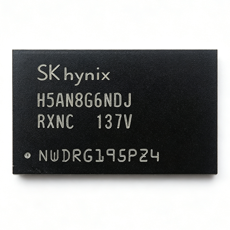
H5AN8G6NDJR-XNC - 8Gb DDR4-3200 x16 DRAM | SK Hynix
The SK Hynix H5AN8G6NDJR-XNC is an 8Gb CMOS Double Data Rate IV (DDR4) Synchronous DRAM organized as 512M x16, operating at a data rate of 3200 Mbps (DDR4-3200). It is housed in a 96-ball FBGA package (13x7.5 mm) and is designed for main memory applications requiring high density and bandwidth. The device supports a supply voltage of 1.2V (VDD) with a maximum of 1.26V, and features auto self-refresh, auto precharge, data mask, dynamic on-chip termination (DTC), ZQ calibration, CRC, write leveling, and asynchronous reset functions. DDR4 SDRAM is a type of volatile random-access memory that transfers data on both edges of the clock, doubling the data rate compared to DDR3. It operates at lower voltages (1.2V) and higher speeds, making it essential for modern computing systems, servers, and embedded applications. As a memory IC, it falls under the hierarchy of DRAM -> SDRAM -> DDR4 -> memory IC -> semiconductor, and is a critical component for data storage and processing. Key features include a 512M x16 organization, 3200 Mbps data rate, 1.2V supply, and a 96-ball FBGA package. The device supports various functions such as auto self-refresh and ZQ calibration, which enhance reliability and signal integrity. The x16 interface allows for high bandwidth per chip, making it suitable for applications requiring wide data paths. Technically, the H5AN8G6NDJR-XNC uses a CMOS process and is fully synchronous, with a differential clock (CK_t/CK_c) and on-die termination for improved signal quality. It supports burst lengths of 8 and 4, and includes a programmable read latency (RL) and write latency (WL) for system optimization. The device also features a temperature-compensated self-refresh (TCSR) to reduce power consumption. Typical applications include laptop and desktop memory upgrades, industrial controllers, networking equipment, and embedded systems. Its high density and speed make it ideal for applications requiring large memory capacity and fast data access, such as AI edge devices and high-performance computing. When designing with this component, ensure proper decoupling capacitors near the VDD and VDDQ pins, and follow the PCB layout guidelines for DDR4 routing to maintain signal integrity. The device is RoHS compliant and lead-free, making it suitable for environmentally conscious designs.
H5AN8G8NCJR-RDC - 8Gb DDR4 SDRAM x8 2666Mbps | SK Hynix
The SK Hynix H5AN8G8NCJR-RDC is an 8Gb (1GB) CMOS Double Data Rate IV (DDR4) Synchronous DRAM organized as x8, operating at 1.2V with data rates up to 2666 Mbps, housed in a 78-ball FBGA package. DDR4 SDRAM is the fourth generation of double-data-rate synchronous dynamic random-access memory, the dominant main-memory technology for servers, workstations, and high-end computing platforms. Within the memory hierarchy, DDR4 sits between the CPU cache and storage, providing the large density and high bandwidth that modern processors demand. DDR4 improved on DDR3 by lowering operating voltage from 1.5V to 1.2V, doubling bank groups to eight, and raising maximum data rates, which reduces system power while increasing effective bandwidth. The H5AN8G8NCJR family offers fully synchronous operation referenced to both rising and falling edges of the clock, with all addresses and control inputs registered on the rising edge of CK. Key features include 8Gb density in a single die, x8 organization, on-die termination (ODT), data mask (DM) support, and JEDEC-standard DDR4 command set. The -RDC suffix denotes the 2666 Mbps speed grade with a commercial operating temperature range. Architecturally, the device uses internal bank groups to allow interleave-friendly access patterns, and a PLL-free design with DLL for output timing alignment. Burst lengths of 8 (BL8) with sequential and interleave options, plus programmable CAS latency, let memory controllers optimize latency versus throughput. The 78-ball FBGA surface-mount package minimizes parasitic inductance, supporting high-speed signal integrity on fly-by-terminated DDR4 channels. Typical applications include server DIMMs and memory-down designs, workstations, industrial computing, networking equipment, and embedded systems requiring large memory density with high bandwidth. The x8 organization suits ECC-based server designs using x8-based chipkill implementations. Design consideration: DDR4 fly-by routing requires length-matched traces, VTT termination, and careful controller training; always validate the speed-grade suffix (-RDC versus -XNC or -VKC) against your controller's supported data rate. This page synthesizes distributor availability, drop-in alternatives within the SK Hynix 8Gb DDR4 family, and JEDEC-compatible cross-brand equivalents, plus practical design notes not found in the raw datasheet.
H5AN8G8NCJR-VKI - DDR4 8Gb 2666Mbps DRAM | SK hynix
The SK hynix H5AN8G8NCJR-VKI is an 8Gb DDR4 SDRAM DRAM chip organized as 1G x8, operating at 2666 Mbps data rate from a 1.2 V supply, housed in a 78-ball FBGA package. It is an industrial-grade ("I" temperature suffix) volatile memory component for main memory and embedded storage designs. DDR4 SDRAM is a synchronous dynamic random-access memory that transfers data on both clock edges (double data rate), providing high bandwidth for processors and SoCs. Within the memory hierarchy it sits as volatile main memory, below non-volatile flash storage and above cache, and is a core building block of power management and memory subsystem design in computing platforms. Key features of the H5AN8G8NCJR-VKI include the 8Gb (1G x8) density, a 2666 Mbps data rate (PC4-21300 class), a 1.2 V core supply that reduces power versus DDR3's 1.5 V, and the compact 78-ball FBGA surface-mount package suited to dense memory layouts. The industrial operating range supports extended-temperature designs where commercial-only DRAM is unsuitable. Technically, the part belongs to the H5AN8G8NCJR-xxC/xI DDR4 SDRAM family, which SK hynix documentation describes as an 8Gb CMOS Double Data Rate IV synchronous DRAM ideally suited for main memory applications requiring large memory density and high bandwidth. The x8 organization allows 78-ball packaging with fewer data lines per device, simplifying layout for 64-bit or ECC-enabled memory controllers. Typical applications include industrial controllers, computing modules, networking equipment, servers, and embedded systems where stable DDR4 sourcing still matters. The industrial grade supports factory automation and edge-computing platforms exposed to harsher thermal environments. When designing with this device, verify controller speed-grade compatibility (2666 Mbps), budget termination and VTT power for the DDR4 bus, and follow SK hynix layout guidance for fly-by clock routing and decoupling on the 1.2 V rail. This page synthesizes distributor stock and pricing data, same-family and cross-brand drop-in alternatives, and practical design notes not found in the manufacturer datasheet.
H5AN8G8NCJR-XNC - 8Gb DDR4-3200 SDRAM, x8, FBGA-78 | SK hynix
The SK hynix H5AN8G8NCJR-XNC is an 8 Gbit DDR4 SDRAM memory IC organized as 1 Gb x 8, rated at the DDR4-3200 speed grade (3200 Mbps data rate, 1.6 GHz clock), operating from a 1.14 V to 1.26 V supply (1.2 V nominal) over a 0 C to +85 C commercial temperature range in a 78-ball FBGA package measuring 7.5 mm x 11 mm. DDR4 SDRAM (Double Data Rate 4 Synchronous Dynamic Random Access Memory) is the fourth generation of the JEDEC DDR memory family. It transfers data on both rising and falling clock edges and introduces a bank-group architecture with multiple internal banks per group, allowing higher effective bandwidth than DDR3 at lower operating voltage. In the system hierarchy, it sits as main-system memory below CPU cache and above storage such as NAND flash and eMMC. Key features of this device include fully synchronous operation referenced to both clock edges, auto self-refresh, auto precharge, an asynchronous reset function, dynamic on-chip termination (ODT), ZQ calibration, write leveling, CRC and CA parity support, and a data mask function. These capabilities simplify high-speed board design and maintain signal integrity at 3200 Mbps rates. The XNC speed grade and its bank-group architecture allow the memory controller to issue commands to different bank groups back-to-back, maximizing effective bandwidth in mainstream DDR4-3200 channels. Low 1.2 V operation reduces power versus DDR3 at equivalent bandwidth, while per-ball power figures of approximately 30 mA and 39 mA (per LCSC/JLCPCB listing) reflect efficient dynamic and standby behavior. Typical applications include desktop and embedded computing main memory, networking equipment line-card memory, industrial controllers, data-storage and logging subsystems, and replacement sourcing for end-of-life DRAM lines in servers and telecom platforms. Design considerations: at DDR4-3200, fly-by routing with per-DIMM or per-component ODT calibration is essential; verify ZQ resistor placement and controller ODT settings, and confirm that the operating temperature stays within the 0 C to +85 C range or enable auto self-refresh derating above 85 C. This page synthesizes distributor pricing, drop-in alternatives, and practical design notes not found in the manufacturer datasheet.
H5AN8G8NDJR - 8Gb DDR4 SDRAM 3200MT/s | SK hynix
The SK hynix H5AN8G8NDJR is an 8Gb CMOS Double Data Rate IV (DDR4) Synchronous DRAM, organized as 1G x 8, operating at a data rate of 3200MT/s (DDR4-3200). It is housed in a 78-ball FBGA package (7.5x11mm) and is designed for main memory applications requiring high density and bandwidth. The device operates from a 1.2V supply (VDD) with a range of 1.14V to 1.26V, and supports a case temperature range of 0°C to +95°C. Key features include auto self-refresh, auto precharge, asynchronous reset, data mask, dynamic on-chip termination (DTC), ZQ calibration, CRC, and write leveling. These features enable robust signal integrity and power efficiency in high-speed systems. DDR4 SDRAM (Double Data Rate Fourth Generation Synchronous Dynamic Random-Access Memory) is a type of volatile memory that transfers data on both rising and falling edges of the clock, doubling the data rate of DDR3. It operates at lower voltages (1.2V vs 1.5V) and offers higher density and speed, making it the standard for modern computing. DDR4 is a key component in the memory hierarchy, sitting between the CPU and storage, and is essential for system performance in PCs, servers, and embedded systems. The H5AN8G8NDJR features a 1G x 8 organization, providing 8Gb of memory in a single chip. It supports data rates up to 3200MT/s, with a CAS latency of 22 (typical) and a tRCD/tRP of 22ns. The device includes on-die ECC (optional) and supports a burst length of 8 and 4 with burst chop. It also features a programmable read latency (RL) and write latency (WL) for system optimization. The FBGA-78 package offers a compact footprint with a 7.5x11mm body, suitable for space-constrained designs. Technically, the H5AN8G8NDJR uses a 20nm-class process technology, enabling high density and low power consumption. It supports a 1.2V supply with a tolerance of ±5%, and includes a VPP supply of 2.5V for wordline boost. The device has a self-refresh current of approximately 30mA (typical) and an active standby current of 60mA. It also features a temperature-compensated self-refresh (TCSR) to reduce power at lower temperatures. The device is RoHS compliant and lead-free. Typical applications include desktop and laptop PCs, servers, networking equipment, and embedded systems. The high bandwidth and low power make it ideal for memory-intensive tasks such as gaming, data analytics, and virtualization. In embedded systems, it provides reliable performance for industrial control and edge computing. When designing with this device, ensure proper decoupling capacitors (0.1uF and 10uF) are placed near the VDD and VDDQ pins. Follow the layout guidelines in the datasheet for signal integrity, especially for the high-speed data and address lines. The ZQ pin requires a 240-ohm resistor to ground for calibration.
H5AN8G8NDJR-XNC - 8Gb DDR4-3200 SDRAM | SK Hynix
The SK Hynix H5AN8G8NDJR-XNC is an 8Gb DDR4 SDRAM memory IC organized as 1G x 8, designed for high-speed, low-voltage memory applications. It operates at a data rate of 3200MT/s (DDR4-3200, PC4-25600) with a supply voltage of 1.2V (VDD) and I/O voltage of 1.2V (VDDQ). The device is housed in a 78-ball FBGA package (7.5x11mm) and is RoHS compliant. It supports an operating temperature range of 0°C to +95°C (TC), making it suitable for a wide range of computing and embedded systems. DDR4 SDRAM (Double Data Rate 4 Synchronous Dynamic Random-Access Memory) is a type of volatile memory that transfers data on both rising and falling edges of the clock signal, effectively doubling the data rate. It is the successor to DDR3 and offers higher speed, lower power consumption, and increased density. DDR4 operates at a lower voltage (1.2V) compared to DDR3 (1.5V), reducing power consumption by up to 40%. It is a critical component in modern computing systems, serving as the main memory for CPUs, GPUs, and SoCs, and is part of the memory hierarchy that includes cache, main memory, and storage. Key features of the H5AN8G8NDJR-XNC include a bank group-based internal architecture that enhances performance, support for standard DDR4 features such as auto self-refresh, auto precharge, asynchronous reset, data mask, dynamic on-chip termination (DTC), ZQ calibration, write leveling, and CRC (Cyclic Redundancy Check) for data integrity. The device also supports on-die ECC (Error Correction Code) in some configurations, though this specific part is a standard non-ECC variant. The 78-ball FBGA package is optimized for high-density PCB layouts, and the device is available in tray packaging. Technically, the H5AN8G8NDJR-XNC implements a 16n prefetch architecture, which is standard for DDR4, allowing it to achieve high bandwidth with a relatively low clock frequency. The device supports a burst length of 8 (BL8) and can be configured for burst chop (BC4). It also supports various power-saving modes, including active power-down, precharge power-down, and self-refresh, which are essential for mobile and embedded applications where power efficiency is critical. The device is designed to operate with a 1.2V supply, and it integrates a temperature sensor for thermal management. Typical applications for the H5AN8G8NDJR-XNC include personal computers, servers, networking equipment, and embedded systems. Its high density and speed make it ideal for main memory in laptops and desktops, while its low power consumption is beneficial for battery-powered devices. In networking, it is used in routers and switches for packet buffering and routing tables. In embedded systems, it is used in industrial controllers, medical devices, and automotive infotainment systems. The device's wide temperature range and reliability make it suitable for industrial applications. When designing with this component, ensure proper decoupling capacitors are placed close to the VDD and VDDQ pins to minimize power supply noise. The device requires a stable 1.2V supply and a reference voltage (VREF) for the I/O. Follow the PCB layout guidelines in the datasheet to maintain signal integrity at 3200MT/s, including controlled impedance traces and proper termination. Also, consider the thermal environment, as the device is rated for up to 95°C case temperature.
H5ANAG6NBJR-PBC - 16Gb DDR4 SDRAM DRAM Chip | SK hynix
The SK hynix H5ANAG6NBJR-PBC is a 16Gb DDR4 SDRAM (Double Data Rate 4 synchronous DRAM) component, offered in a compact FBGA-96 ball-grid-array package for high-density main memory subsystems. DDR4 SDRAM is the mainstream generation of DRAM used as main system memory in PCs, servers, embedded controllers and networking equipment. Within the memory hierarchy it sits between caches/SSDs and storage, providing the large, fast working set that processors demand. The H5ANAG family belongs to SK hynix's 16Gb DDR4 portfolio, which the manufacturer positions as major DRAM for advanced compute, offering higher configurable densities than previous generations. Key characteristics of this family include a 16Gb (2 GB) density per die, DDR4 architecture operating at a nominal 1.2 V supply - roughly 20% lower operating voltage than DDR3, reducing power per bit - and data rates up to the DDR4 generation maximum of 3200 MT/s across the portfolio. Verified family features include auto self-refresh, data mask (DM) function, asynchronous reset, dynamic on-chip termination (ODT), ZQ calibration, write leveling and CRC function. Technically, the device is a CMOS DDR4 SDRAM implementing bank-group architecture with internal prefetch, supporting the JEDEC DDR4 feature set including bank groups, posted CAS and command/address training modes. The -PBC speed/temp code denotes a specific validated speed bin; verify the exact MT/s bin against the official SK hynix datasheet before final design sign-off. Typical applications include main memory for desktop and notebook platforms, embedded computing modules, industrial controllers, networking line cards and set-top or consumer electronics that use x16 DDR4 memory down on the baseboard. A key design consideration: DDR4 routing requires careful length matching of DQ/CA lines, correct VTT termination with dynamic ODT, and ZQ resistor placement; the 96-ball layout also constrains via fan-out, so plan layer stack-up early. This page synthesizes verified web data, family feature sets, drop-in alternative candidates and practical design notes in one place - information not consolidated in the manufacturer datasheet.
H5ANAG6NBJR-VKC - 16Gb DDR4 SDRAM 2666Mbps | SK Hynix | Memory IC
The SK Hynix H5ANAG6NBJR-VKC is a 16Gb (2GB) DDR4 SDRAM component rated for 2666 Mbps data rate, organized with a x16-wide data interface and housed in a 96-ball FBGA (PBGA96) surface-mount package. It belongs to SK Hynix's DDR4 SDRAM family of high-density dynamic random access memories used in computing, industrial, and consumer platforms. DDR4 SDRAM (Double Data Rate fourth-generation Synchronous Dynamic Random Access Memory) is the mainstream volatile memory technology bridging the processor and storage hierarchy. In the memory hierarchy, DDR4 DRAM sits below CPU caches and above SSD/NAND storage, providing high-bandwidth working memory. It evolved from DDR3 by lowering the core voltage from 1.5V to 1.2V, raising bank-group parallelism, and introducing features such as a dynamic on-chip termination (ODT) scheme, ZQ calibration, write leveling, CRC for command/address integrity, and asynchronous reset, all of which this SK Hynix family supports. Key features of the H5ANAG6NBJR family include the 16Gb die density on advanced process nodes, 1.2V operation, auto self-refresh and self-refresh temperature operation across an industrial-relevant range of -40C to +95C (per the related VKC-grade SK Hynix DDR4 components listed by LCSC), data mask (DM) functionality, and CRC/ACTM-based signal integrity features for reliable multi-DIMM operation. Architecturally, this 16Gb DDR4 device uses bank groups with internal prefetch to sustain the 2666 Mbps DDR4 data rate while managing refresh overhead. On-die termination and driver strength calibration (ZQ) maintain eye margins on high-speed address/command and data buses, enabling robust operation on dense PCB stacks. Typical applications include industrial PCs and embedded controllers, network appliances and routers, set-top boxes and smart TVs, and gaming/consumer computing boards where high density per component reduces part count and BOM size. Design consideration: DDR4 routing demands length-matched fly-by or point-to-point topologies, controlled impedance, and careful VDDQ plane decoupling; verify the exact speed bin and temperature grade against the full SK Hynix datasheet before layout sign-off. This page adds engineering value beyond the datasheet by consolidating drop-in same-footprint alternates from the same SK Hynix DDR4 family, distributor stock signals, and practical layout guidance for the 96-ball FBGA footprint. Pricing shown is indicative as of 2026-09-04.
H5ANAG6NCJR-XN - 16Gb DDR4-3200 SDRAM FBGA-96 | SK hynix
The SK hynix H5ANAG6NCJR-XN is a 16 Gigabit (1G x 16) DDR4 SDRAM rated for DDR4-3200 (3200 Mbps/pin) operation, powered from a 1.14V to 1.26V supply and housed in a 96-ball FBGA package approximately 8 mm wide. It belongs to SK hynix's G6-generation 16Gb DDR4 DRAM family and is designed for high-density main memory subsystems. DDR4 SDRAM (Double Data Rate 4 Synchronous Dynamic Random Access Memory) is the fourth generation of the DDR DRAM hierarchy: DRAM -> synchronous DRAM -> DDR SDRAM -> DDR4 SDRAM, a memory-class semiconductor used as the working memory of processors and controllers. Compared with DDR3, DDR4 lowers operating voltage to roughly 1.2V, doubles bank groups, and raises data rates well beyond 3200 Mbps, improving bandwidth per watt. Key features of this device include an auto self-refresh mode for low-power data retention, an auto precharge function, an asynchronous reset function for reliable initialization, a data mask (DM) function for selective byte writes, dynamic on-chip termination (ODT), and a ZQ calibration function that trims output driver strength against process and temperature variation. A CRC function supports command/address integrity and write leveling supports fly-by memory topology timing. Architecturally, the device is organized as 1G addresses of 16-bit words, arranged in bank groups that allow interleaved access for higher effective bandwidth. The 16-bit organization suits systems that populate two or four chips per 32/64-bit memory channel, common in embedded x86 and ARM designs. The -XN speed grade marks DDR4-3200 timing (per SK hynix speed-bin tables in the manufacturer datasheet). Typical applications include industrial controllers and embedded computing modules, network and communication equipment line cards, test and measurement instrumentation, and replacement/extension sourcing for legacy DDR4-based board designs that require 16Gb x16 density at DDR4-3200. For design, route address/command buses with fly-by topology, terminate with dynamic ODT, and follow the manufacturer datasheet for ZQ calibration resistor placement (240 ohm 1%) and power-rail sequencing between VDD and VDDQ rails. This page synthesizes distributor stock, pricing, drop-in alternatives, and practical DDR4 design notes not found in the manufacturer datasheet alone.
H5ANAG6NCJR-XNC - 16Gb DDR4-3200 SDRAM x16 | SK Hynix
The SK Hynix H5ANAG6NCJR-XNC is a 16Gb (1G x 16) DDR4 SDRAM memory IC operating at DDR4-3200 data rates from a 1.14V to 1.26V supply, housed in a 96-ball FBGA (PBGA) package. DDR4 SDRAM (Double Data Rate 4 Synchronous Dynamic Random Access Memory) is the fourth generation of the DDR DRAM family, a class of volatile memory ICs that transfer data on both clock edges to achieve high bandwidth. In the memory hierarchy, DRAM sits between CPU caches and non-volatile storage such as NAND flash, serving as the primary working memory in computing systems. DDR4 doubled bank counts versus DDR3, lowered operating voltage from 1.5V to 1.2V, and added features such as bank grouping and a DBI (data bus inversion) option. Key features of this device include auto self-refresh, auto precharge, asynchronous reset, data mask (DM) function for x16 operation, dynamic on-chip termination (ODT), ZQ calibration, CRC function, and write leveling - all of which improve signal integrity and simplify high-speed memory controller interfacing. The x16 organization suits systems that do not require dedicated ECC devices, allowing one chip per 16-bit data lane. The -XNC speed bin supports 3200 Mbps/pin data rates at a CAS latency appropriate for DDR4-3200 operation, delivering roughly 51.2 Gb/s of peak bandwidth per component at full rate. The 96-ball FBGA surface-mount package keeps inductance low, which is essential at 3200 Mbps where trace-length matching, reference VDDQ planes, and on-die termination determine timing margin. Typical applications include industrial controllers and embedded computing modules, networking equipment line cards, set-top boxes, smart TVs, and replacement sourcing for legacy DRAM DIMM/module designs. The 16Gb density is well suited to designs needing 2 GB or more per component without the complexity of ECC with x8 parts. When designing with this part, keep fly-by or point-to-point topologies length-matched, verify the memory controller supports 16-bit data mask operation, and follow the JEDEC DDR4 power-ramp sequencing requirements for VDD, VDDQ, and VPP rails. This page synthesizes distributor pricing, same-package drop-in alternatives, and practical design notes not found in the manufacturer datasheet, with data verified as of 2026-09-04.
H5ANAG6NCMR-XNC - 16Gb DDR4 SDRAM x16 FBGA-96 | SK Hynix
The SK Hynix H5ANAG6NCMR-XNC is a 16Gb (1G x 16) CMOS DDR4 Synchronous DRAM operating at a 3200 Mbps data rate from a 1.2V core supply, housed in a 96-ball FBGA package. DDR4 SDRAM (Double Data Rate 4 Synchronous Dynamic Random Access Memory) is the fourth generation of the DDR DRAM family, a class of volatile memory that transfers data on both clock edges and synchronizes operation to a system clock. Within the memory hierarchy, DDR4 SDRAM sits below DDR5 and above DDR3, and serves as main memory in the broader power and data management IC ecosystem for computing systems. Key features of the H5ANAG6NCMR-XNC include its large 16Gb density organized as 1G words of 16 bits, a 3200 Mbps/pin transfer rate suitable for high-bandwidth main memory, a low 1.2V operating voltage that reduces dynamic power versus DDR3, and the space-saving FBGA (Fine-Pitch Ball Grid Array) package. The XN speed bin designation indicates the 3200 Mbps grade; the CMR suffix denotes standard CMOS DRAM process. Technically, DDR4 SDRAMs like this device use an 8n prefetch architecture, bank groups, and programmable CAS latency to sustain high effective bandwidth while managing access latency. Per SK hynix product documentation, the H5ANAG6NCMR family is ideally suited for main memory applications that require large memory density and high bandwidth, with normal power classification and 1.2V operation. Typical applications include desktop and notebook PC main memory modules, servers and embedded computing boards, industrial controllers requiring large volatile storage, and networking equipment data buffers. When designing with this device, ensure the memory controller supports DDR4-3200 timing and that fly-by routing, on-die termination, and power delivery for the 1.2V VDD rail follow JEDEC DDR4 layout practice. This page synthesizes distributor pricing, drop-in alternatives, and practical design notes not found in the manufacturer datasheet.
H5ANAG6NCR-PBC - 16Gb DDR4 SDRAM x16, FBGA-96 | SK hynix
The SK hynix H5ANAG6NCR-PBC is a 16Gb (2GB) DDR4 SDRAM organized as x16 with a 16-bit data interface, supplied over a nominal 1.2V power rail (1.14V to 1.26V operating window) and housed in a 96-ball FBGA package. The H5ANAG6 family is documented by SK hynix with a transfer class of 3200 Mbps, automatic self-refresh, auto precharge, asynchronous reset, data mask, dynamic on-chip termination (ODT), ZQ calibration, CRC, and write leveling functions. DDR4 SDRAM is the fourth generation of Double Data Rate synchronous dynamic random-access memory, a class of volatile memory ICs that sits within the broader memory hierarchy of semiconductor devices. DDR4 doubles the internal bank count of its DDR3 predecessor, lowers the operating voltage from 1.5V to 1.2V, and adds bank-group architecture, giving designers higher bandwidth with lower power per transferred bit. A 16Gb monolithic die reduces component count per gigabyte versus stacked smaller dies. Key features of this family include the 1.14V to 1.26V supply window that eases power-tree design, dynamic ODT for signal integrity on heavily loaded buses, and write leveling with ZQ calibration that simplifies high-speed PCB routing. The CRC function protects data integrity on the write path, while asynchronous reset enables deterministic power-up and error recovery. Architecturally, the die uses bank-group parallelism so multiple banks can be interleaved within one burst window, sustaining high bus utilization. The x16 organization pairs well with 32-bit or 64-bit memory controllers using two or four devices, common in embedded and networking designs that do not need the module DIMM form factor. Typical applications include embedded motherboards, industrial controllers, networking and telecom line cards, and consumer electronics boards built around DDR4 controllers from FPGA or processor vendors such as Intel (Altera) FPGA families. Design considerations: adhere to the JEDEC DDR4 fly-by routing topology, length-match the data groups, and complete ZQ calibration during initialization; the exact speed grade designation and CAS latency for the PBC suffix are not stated in the retrieved data, so verify against the official SK hynix datasheet before finalizing controller timing. This page synthesizes distributor availability data, same-package drop-in family alternatives, and practical design guidance beyond the raw manufacturer datasheet, giving engineers a faster path from selection to layout.
H5ANAG6NCR-RDC - 16Gb DDR4 SDRAM 3200Mbps x16 | SK Hynix
The SK Hynix H5ANAG6NCR-RDC is a 16Gb (2GB) DDR4 SDRAM organized as 1G x 16, supporting data transfer rates up to 3200 Mbps at a nominal 1.2V core supply, housed in a 96-ball FBGA surface-mount package. DDR4 SDRAM (Double Data Rate Fourth Generation Synchronous Dynamic Random Access Memory) is the dominant main-memory technology for servers, workstations, embedded computing, and networking equipment. As a class of volatile semiconductor memory, DDR4 DRAM sits within the broader memory hierarchy of DRAM -> volatile memory -> semiconductor memory, succeeding DDR3 with lower operating voltage (1.2V vs 1.5V), higher bank counts (16 banks via bank groups), and improved signaling using DBI (Data Bus Inversion), CRC, and CA parity. Key features of the H5ANAG6NCJR device family include auto self-refresh, auto precharge function, asynchronous reset function, data mask (DM) function, dynamic on-chip termination (ODT), ZQ calibration, CRC function, and write leveling. The x16 organization suits designs with narrower memory buses such as embedded processors, networking line cards, and industrial controllers. Architecturally, this 16Gb die uses DDR4 bank-group architecture enabling back-to-back data access within a bank group at the internal core rate, sustaining the 3200 Mbps (PC4-25600 class) interface speed. The 96-ball FBGA (8 mm width rectangular body) minimizes footprint and parasitic inductance for high-speed signal integrity. Internal arrays operate from a separated VDD core supply while the DQ bus supports programmable termination. Typical applications include networking and telecom equipment, industrial automation controllers, embedded computing modules, test and measurement systems, and server-memory modules where 16-bit-wide DDR4 channels are required. When designing with this device, observe JEDEC DDR4 routing practices: length-match DQ/DM/UDQS byte groups within ±25 mils, series-terminate the clock and strobes, and implement the asynchronous RESET pin correctly so the device remains in a known state during power sequencing. Confirm speed-grade suffix (RDC) compatibility with your memory controller calibration settings. This page synthesizes distributor inventory and pricing, drop-in SK Hynix family alternatives, and practical DDR4 design notes not consolidated in the manufacturer datasheet. Pricing references are as of 2026-09-05.
H5ANAG6NCR-XNC - 16Gb DDR4 SDRAM FBGA-96 | SK Hynix
The SK Hynix H5ANAG6NCR-XNC is a 16Gbit DDR4 SDRAM (DRAM) memory IC organized as 1G x 16, operating at a VDD of 1.14V to 1.26V (1.2V nominal VDD/VDDQ class), housed in a 96-ball FBGA package. It belongs to the 8Gbit-per-die-generation H5ANAG6 family of DDR4 SDRAMs used for main memory and buffering in computing and industrial systems. DDR4 SDRAM (Double Data Rate 4 Synchronous Dynamic Random Access Memory) is the fourth generation of DDR memory, defined around a low-voltage 1.2V signaling environment, internal bank grouping, and higher data rates than DDR3. In the memory hierarchy it sits as a volatile main-memory device below CPU caches and above storage (NAND/EEPROM), and it is a core power-management-relevant load in any processor-based system. Key features verified for the H5ANAG6NCJR sibling (shared family datasheet) include auto self-refresh, auto precharge function, asynchronous reset function, data mask function, dynamic on-chip termination (ODT), ZQ calibration, CRC function, and write leveling. These features improve signal integrity on high-speed point-to-point DDR4 buses and simplify controller bring-up. Architecturally, DDR4 devices use internal bank groups with independent activation, burst length 8 (BL8) access, and on-die termination networks calibrated against a precision external ZQ resistor. The x16 organization provides a 16-bit wide data interface with data mask (DM) pins for partial writes, suiting designs that need narrower buses or higher per-device bandwidth granularity than x8 or x4 parts. Typical applications include embedded computing modules, industrial controllers, network appliances, test and measurement instrumentation, and replacement sourcing for DDR4-based main-memory sockets where 16Gb x16 devices are specified in the BOM. Design consideration: DDR4 routing demands length-matched, impedance-controlled traces with proper fly-by or point-to-point topology, and VREF/ODT settings must be tuned per the controller memory training results; supply decoupling of the 1.2V rail with low-ESR ceramics is mandatory. This page synthesizes distributor pricing, drop-in family alternatives, and practical design notes not found in the manufacturer datasheet, with pricing as of 2026-09-05.
H5ANAG8NCJR-XNC - 16Gb DDR4-3200 SDRAM 2Gx8 | SK Hynix
The SK Hynix H5ANAG8NCJR-XNC is a 16Gb (2G x 8) DDR4 SDRAM rated for DDR4-3200 data rates, operating from a 1.2 V supply in a 78-ball FBGA (7.5 x 11 mm) package qualified for the 0C to +95C commercial temperature range. A DDR4 SDRAM (Double Data Rate Fourth Generation Synchronous Dynamic Random Access Memory) is the mainstream volatile main-memory technology for computing systems. In the memory hierarchy, DRAM sits between CPU caches (SRAM) and persistent storage (NAND flash / SSDs), providing high-bandwidth working memory. DDR4 doubled the internal bank count of DDR3 (16 banks in 4 bank groups) and lowered the I/O voltage from 1.5 V to 1.2 V, improving bandwidth per watt. A DRAM controller inside the host SoC or memory controller manages refresh, bank interleaving, and DDR4 protocol timing, so this chip is never used standalone - it is soldered to a memory bus alongside a processor, FPGA with hard memory controller, or memory-companion chip. Key features include 16 Gbit density per monolithic die, an x8 organization (2G addressable words x 8 bits), and DDR4-3200 operation (3200 MT/s), yielding up to 25.6 GB/s of peak bandwidth per 64-bit channel when populated 8-deep. The XNC speed grade is specified over 0C to +95C. Per TechInsights teardown analysis, the H5ANAG8NCJR-XNC contains the H5ANAG6NC die, SK hynix's first 1z nm node DRAM, offering the smallest 16Gb DDR4 die size and highest bit density (0.296 Gb/mm2) of its generation, built on non-EUV lithography. Architecturally, DDR4 devices use a multi-bank-group array with bank-group-wise row activation, a DLL for output timing, and on-die VDDQ termination (ODT) to preserve signal integrity at 3200 MT/s. The 1z nm process shrinks the cell transistor and capacitor, reducing standby and active current versus earlier 1x/1y nm parts. Typical applications include industrial controllers and computing modules requiring large memory density, firmware boot and embedded logging buffers, SSD controller write caches, and replacement sourcing for DDR4-based main memory on servers, workstations, and networking line cards. Design consideration: DDR4-3200 routing requires length-matched fly-by termination and careful DQS/DQ skew budgeting; always tie CA parity and alert pins per the JEDEC DDR4 convention and your memory controller's compatibility guide. This page synthesizes distributor pricing and stock, drop-in same-family alternatives, and practical design notes not found in the manufacturer datasheet.
H5ANAG8NCMR-VKI - 16Gb DDR4 SDRAM 2666Mbps x8 | SK Hynix
The SK Hynix H5ANAG8NCMR-VKI is a 16Gb CMOS Double Data Rate IV (DDR4) synchronous DRAM organized as x8, operating at data rates up to 2666 Mbps per pin, supplied in a space-saving FBGA (fine-pitch ball grid array) package designed for main memory applications requiring large density and high bandwidth. DDR4 SDRAM is the fourth generation of Double Data Rate synchronous DRAM, a class of volatile memory that transfers data on both rising and falling edges of the clock, doubling effective bandwidth compared to SDR DRAM. In the system memory hierarchy, DDR4 sits below LPDDR4/DDR5 in power optimization but above DDR3 in speed and density, making it the dominant main-memory technology for servers, workstations, and embedded compute platforms from roughly 2014 to the present DDR5 transition. Key features of the H5ANAG8NCMR-VKI include fully synchronous operation referenced to both rising and falling edges of the clock, differential clock inputs (CK/CK#) for improved signal integrity, and on-die termination (ODT) that reduces reflections on high-speed address, command, and data buses. The 16Gb density in a single x8 component allows designers to populate 8GB with only four devices, reducing BOM count and PCB area compared to lower-density generations. Technically, the device uses a bank-group architecture with multiple internal banks, supporting commands such as ACTIVATE, READ, WRITE, and PRECHARGE per the JEDEC DDR4 specification, with programmable CAS latency and burst length for system tuning. The -VKI speed grade supports 2666 Mbps operation with JEDEC-standard 1.2V VDD signaling, enabling lower power than DDR3's 1.5V interface at substantially higher bandwidth. Typical applications include server and workstation main memory DIMMs, industrial embedded computing modules, networking equipment line-card buffers, and FPGA-based processing systems that require gigabyte-scale working memory with high sustained bandwidth. When designing with this device, pay close attention to DDR4 fly-by routing, VREF training, and ZQ calibration requirements, which differ significantly from DDR3 layouts and are critical for signal integrity at 2666 Mbps. This page synthesizes distributor stock data, drop-in alternatives, and practical design notes not found in the manufacturer datasheet, giving buyers and engineers a single decision-ready reference.