Memory ICs
Subcategories
Products (487)
H5TC4G63CFR-xxL - 4Gb DDR3L SDRAM 256Mx16 | SK Hynix
The H5TC4G63CFR-xxL is a 4Gb low power Double Data Rate III (DDR3L) Synchronous DRAM manufactured by SK Hynix. It is organized as 256M x 16 and operates at a low voltage of 1.35V, making it ideal for main memory applications that require large memory density, high bandwidth, and low power operation. The device is lead-free and halogen-free, compliant with RoHS standards, and is available in a 96-pin FBGA package. DDR3L SDRAM is a type of dynamic random-access memory that operates at a lower voltage (1.35V) compared to standard DDR3 (1.5V), reducing power consumption by approximately 20% while maintaining backward compatibility with DDR3-based environments. It is part of the DDR3 memory family, which uses double data rate signaling to transfer data on both edges of the clock, achieving high bandwidth. DDR3L is commonly used in laptops, embedded systems, and networking equipment where power efficiency is critical. Key features of the H5TC4G63CFR-xxL include a 4Gb density, 256M x 16 organization, 1.35V power supply, and support for data rates up to 2133 Mbps (depending on the speed grade). The device offers low power consumption, with a typical operating current of [DATA_NEEDED: IDD0] and standby current of [DATA_NEEDED: IDD2P]. It also features on-die termination (ODT), programmable CAS latency, and burst lengths of 8 and 4 (with burst chop). The device is designed for reliable operation over a temperature range of [DATA_NEEDED: operating temperature range]. The H5TC4G63CFR-xxL utilizes advanced DRAM process technology, providing high density and performance while minimizing power consumption. The 96-pin FBGA package offers excellent thermal and electrical characteristics, supporting high-speed signaling with minimal parasitic inductance. The device includes auto-refresh and self-refresh modes to maintain data integrity with minimal power draw. Typical applications include main memory for laptops and ultrabooks, embedded systems, networking equipment, and industrial computing. The low voltage and high bandwidth make it suitable for power-sensitive designs that require high performance. The device is also used in memory modules and system-on-module (SoM) designs. When designing with this component, ensure proper decoupling capacitors are placed near the power pins to minimize noise. The DDR3L interface requires careful PCB layout to maintain signal integrity, including matched trace lengths and controlled impedance. Refer to the SK Hynix datasheet for detailed design guidelines and timing parameters.
H5TC4G63MFR-PBA - 4Gb DDR3L SDRAM 256Mx16 | SK hynix
The H5TC4G63MFR-PBA is a 4Gb DDR3L SDRAM organized as 256M x 16, manufactured by SK hynix. It operates at a supply voltage of 1.35V (VDD and VDDQ) with a range of +0.100V/-0.067V, and is housed in a 96-ball FBGA package. This memory device supports data rates up to 1866 Mbps (PC3L-14900) and is designed for low-power applications, offering a significant reduction in power consumption compared to standard DDR3. DDR3L SDRAM (Double Data Rate 3 Low Voltage) is a type of synchronous dynamic random-access memory that operates at 1.35V, reducing power consumption by about 20% compared to standard 1.5V DDR3. It is part of the DDR3 family, which uses double data rate architecture to transfer data on both edges of the clock, achieving high bandwidth. DDR3L is commonly used in mobile devices, embedded systems, and enterprise servers where power efficiency is critical. Key features include a 16-bit I/O configuration, 8 internal banks, and support for various burst lengths (BL8 and BL4 with burst chop). The device includes on-die termination (ODT), ZQ calibration, write leveling, and dynamic ODT for improved signal integrity. It also supports auto self-refresh and a temperature-compensated self-refresh rate to minimize standby power. The H5TC4G63MFR-PBA uses a 30nm-class process technology, enabling high density with low power. It features programmable CAS latency (CL), CAS write latency (CWL), and additive latency, allowing flexibility in system timing. The device is compliant with JEDEC DDR3L standards, ensuring interoperability with a wide range of controllers. Typical applications include mobile computing, networking equipment, industrial automation, and embedded systems where low power and high performance are required. Its 256Mx16 organization is ideal for systems needing a single high-density memory chip with a 16-bit data bus. When designing with this device, ensure proper decoupling capacitors near the power pins and follow the PCB layout guidelines in the datasheet to maintain signal integrity at high speeds. The device requires a stable 1.35V supply and careful termination of the address/control bus.
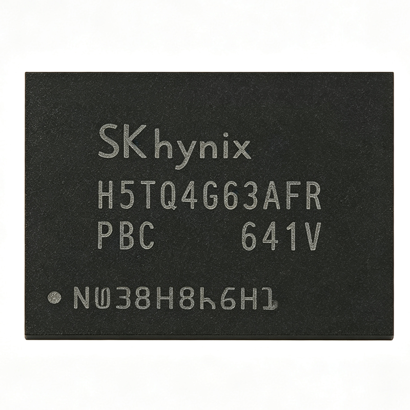
H5TQ4G63AFR-H9C - 4Gb DDR3 SDRAM 256Mx16 | SK Hynix
The H5TQ4G63AFR-H9C is a 4Gb CMOS Double Data Rate III (DDR3) Synchronous DRAM from SK Hynix, organized as 256M x 16. It operates at a clock speed of 0.255ns (tCK) and is packaged in a 96-ball TFBGA (Thin Fine-Pitch Ball Grid Array) with a rectangular shape. This device is designed for main memory applications requiring high density and bandwidth, offering fully synchronous operations referenced to both rising and falling edges of the clock. It supports a supply voltage of 1.5V and features 8192 refresh cycles, ensuring data integrity in high-performance computing environments. DDR3 SDRAM (Double Data Rate Type 3 Synchronous Dynamic Random-Access Memory) is a type of memory that transfers data on both edges of the clock signal, effectively doubling the data rate compared to single-data-rate SDRAM. It is a key component in the memory hierarchy, serving as the main system memory in computers, servers, and embedded systems. DDR3 is the successor to DDR2 and offers higher bandwidth and lower power consumption, making it suitable for a wide range of applications from consumer electronics to enterprise data centers. Key features of the H5TQ4G63AFR-H9C include a 4Gb density, 256M x 16 organization, and a 96-ball TFBGA package. It is halogen-free and RoHS compliant, meeting environmental standards. The device operates with a 1.5V power supply and supports a data rate of 0.255ns (approximately 3.9 Gbps per pin). The refresh cycle count of 8192 ensures reliable operation over extended periods. The package is designed for surface mount technology, enabling compact and high-density PCB layouts. Technically, the H5TQ4G63AFR-H9C utilizes advanced CMOS process technology to achieve high speed and low power. It features programmable CAS latency, burst length, and other timing parameters via the mode registers, allowing system designers to optimize performance. The device supports on-die termination (ODT) and dynamic ODT for improved signal integrity, which is critical at high data rates. The 96-ball TFBGA package provides excellent thermal and electrical performance, with a ball pitch of 0.8mm, facilitating routing and manufacturing. Typical applications for the H5TQ4G63AFR-H9C include desktop and laptop computers, servers, networking equipment, and embedded systems that require high-capacity, high-bandwidth memory. Its 256M x 16 organization is ideal for systems with a 16-bit data bus, such as many microprocessors and SoCs. The device's low power consumption and high reliability make it suitable for both consumer and industrial applications. When designing with this DDR3 SDRAM, it is essential to ensure proper signal integrity by following the layout guidelines for high-speed memory interfaces, including controlled impedance traces, proper termination, and decoupling. The memory controller must be configured to match the device's timing parameters, such as CAS latency and burst length, to achieve optimal performance. Additionally, thermal management should be considered, as high-speed operation can generate significant heat.
HMCG78CGBSA095N - 16GB DDR5-5600 SODIMM 1Rx8 | SK hynix
The SK hynix HMCG78CGBSA095N is a 16GB DDR5 SODIMM memory module operating at 5600 MT/s (PC5-44800), with CL46 latency at 1.1 V, built on a 1Rx8 organization in a 262-pin unbuffered non-ECC SODIMM package. It uses eight 2Gx8 DDR5 DRAM components (8C configuration) validated to the DDR5-5600B speed bin. A SODIMM (Small Outline Dual In-line Memory Module) is a compact memory module form factor designed for space-constrained systems such as laptops, mini PCs, and embedded platforms. Within the memory hierarchy, it belongs to the DDR5 DRAM module family - the successor to DDR4 - delivering double the bank groups, on-module power management, and higher data rates than the 3200 Mbps typical of DDR4 SODIMMs. Key features of the HMCG78CGBSA095N include the DDR5-5600 data rate per the JEDEC DDR5 standard, PC5-44800 bandwidth class, and a CAS latency of 46 at 1.1 V operation. The 1Rx8 single-rank organization simplifies memory controller training and can reduce power draw compared to dual-rank configurations of the same capacity. Technical architecture: the module integrates eight 2Gb x8 DDR5 SDRAM die per the 8C stacking scheme, an on-module 5V-to-1.1V PMIC (Power Management IC) that moves voltage regulation off the motherboard, and an SPD hub that stores training data and serial presence detect information for the host BIOS. Typical applications include laptop and notebook memory upgrades, mini PC and small-form-factor desktops, industrial computing platforms, and test equipment requiring 16GB of DDR5 SODIMM memory with 5600 MT/s throughput. Design consideration: verify host-platform support for DDR5-5600 SODIMMs and ensure BIOS/SPD compatibility before deployment; mixing modules of different ranks or speed bins may force downclocking to the lowest common denominator. This page synthesizes distributor availability, drop-in same-footprint alternatives, and practical upgrade guidance not found on a single manufacturer page. Pricing and stock data reflect distributor listings as of 2026-09-05.
HMCG78MEBRA113N - 16GB DDR5-4800 ECC RDIMM | SK hynix
The SK hynix HMCG78MEBRA113N is a 16GB DDR5 ECC Registered DIMM (RDIMM) memory module operating at 4800 MT/s (PC5-38400) with CL40 latency at 1.1V, in a 288-pin DIMM form factor with a 1Rx8 (single rank, x8) organization. A registered (buffered) DIMM is a server-class memory module that places a register between the DRAM arrays and the memory controller, reducing electrical load on the command/address lines and enabling higher module counts per channel than unbuffered desktop UDIMMs. RDIMMs sit within the memory module hierarchy (DRAM IC -> module -> registered DIMM -> enterprise memory subsystem) and are the standard memory type for servers and workstations, distinguishing them from unregistered ECC SODIMMs and consumer UDIMMs. Key features of the HMCG78MEBRA113N include its 16GB capacity per module, 4800 MT/s data rate certified as PC5-38400, and on-module ECC registered architecture that corrects single-bit memory errors for data integrity in always-on enterprise systems. The 1.1V operating voltage follows the JEDEC DDR5 standard, delivering lower power per bit transferred than DDR4 RDIMMs of equivalent capacity. The 1Rx8 single-rank organization keeps command scheduling simple for the memory controller and suits dense multi-DIMM-per-channel server boards. Technically, the module uses DDR5 DRAM devices with on-die ECC and a side-band management interface, and the register/buffer logic decouples command/address signaling so the module meets JEDEC DDR5 RDIMM timing at 4800 MT/s with CL40 (40-40-40 typical JEDEC scaling). Backward compatibility to 4400 MT/s is supported on platforms whose memory controllers negotiate lower speeds. Typical applications include enterprise servers based on Intel Xeon Scalable 4th/5th Gen and AMD EPYC processors, such as HPE ProLiant Gen10+/Gen11, Dell PowerEdge 16G series, and Lenovo ThinkSystem platforms, as well as virtualization hosts and data-intensive workloads where ECC protection is mandatory. When designing or configuring systems, populate DIMM slots per the server vendor's population rules for single-rank RDIMMs and confirm that the platform BIOS supports 4800 MT/s; otherwise the module will downclock gracefully to the highest mutually supported JEDEC speed. This page synthesizes distributor pricing, stock data, drop-in alternative module numbers, and platform compatibility notes not found in a single manufacturer datasheet.
IS43QR16512B-062AABL - 8Gb DDR4 SDRAM 512Mx16 | ISSI
The IS43QR16512B-062AABL is an 8Gb DDR4 SDRAM organized as 512Mx16, operating from a 1.2V supply. It supports data transfer rates up to 3200 MT/s with a CAS latency of 22-22-22, and is housed in a 96-ball TWBGA package (7.5mm x 13.5mm). This memory IC is designed for high-performance computing, networking, and industrial applications requiring high bandwidth and low power consumption. DDR4 SDRAM (Double Data Rate 4 Synchronous Dynamic Random-Access Memory) is a type of volatile memory that transfers data on both edges of the clock signal, doubling the data rate compared to DDR3. It uses an 8n prefetch architecture, enabling high-speed data transfer while maintaining lower power consumption through a reduced supply voltage of 1.2V. DDR4 is the industry standard for main memory in servers, desktops, and embedded systems, offering improved speed, density, and reliability over previous generations. Key features include a 1.2V power supply, 3200 MT/s data rate, 19ns tRCD (RAS-to-CAS delay), and a 96-ball TWBGA package. The device supports on-die termination (ODT), programmable read/write latencies, and auto-refresh and self-refresh modes. It is RoHS compliant and operates over a temperature range of 0°C to +95°C (case temperature). The IS43QR16512B uses a high-speed CMOS process and an 8n prefetch architecture, which allows two data words to be transferred per clock cycle at the I/O pins. This design achieves high bandwidth while minimizing power consumption. The device includes a mode register for programming various operating modes, including burst length, CAS latency, and test modes. It also supports error correction code (ECC) for enhanced data integrity in critical applications. Typical applications include high-performance servers, networking equipment (routers, switches), data centers, and industrial computing systems. The high density and speed make it suitable for memory-intensive tasks such as virtualization, real-time analytics, and high-frequency trading. Its low power consumption is beneficial for power-constrained embedded systems. When designing with this DDR4 SDRAM, ensure proper signal integrity by maintaining controlled impedance traces and using appropriate termination. The device requires a stable 1.2V supply and a separate VTT termination voltage. Follow the manufacturer's layout guidelines for the 96-ball TWBGA package to minimize crosstalk and ensure reliable operation at 3200 MT/s.
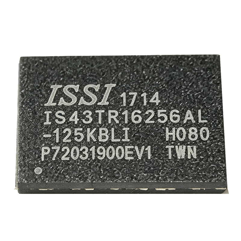
IS43TR16256A-125KBL - 4Gb DDR3 SDRAM 256Mx16 | ISSI
The IS43TR16256A-125KBL is a 4Gbit DDR3 SDRAM organized as 256M x 16, manufactured by Integrated Silicon Solution Inc (ISSI). It operates at a standard voltage of 1.5V (VDD and VDDQ) with a data rate of 1600MT/s (800 MHz clock), and is available in a 96-ball TWBGA (9x13mm) package. This memory IC is designed for high-speed data transfer in computing, networking, and industrial applications. DDR3 SDRAM (Double Data Rate Type 3 Synchronous Dynamic Random-Access Memory) is a type of volatile memory that transfers data on both edges of the clock signal, effectively doubling the data rate compared to DDR2. It is a key component in systems requiring high bandwidth and low latency, such as servers, routers, and embedded processors. DDR3 operates at lower voltages (1.5V or 1.35V for DDR3L) than previous generations, reducing power consumption. Key features include a 4Gbit density, 16-bit I/O width, 800 MHz clock frequency, and a CAS latency of 11 (CL=11) at 1600MT/s. The device supports on-die termination (ODT), programmable CAS latency, and burst lengths of 8 and 4 (with burst chop). It also features auto refresh and self refresh modes for power saving. The 96-ball TWBGA package provides a compact footprint suitable for space-constrained designs. The IS43TR16256A-125KBL uses a high-performance CMOS process and includes a DLL (Delay-Locked Loop) for precise timing alignment. It supports a burst length of 8 with a burst chop of 4, and features programmable read and write latencies. The device also includes a temperature-compensated self-refresh (TCSR) mode to reduce power consumption at high temperatures. Typical applications include main memory for embedded systems, networking equipment (routers, switches), industrial PCs, and high-performance computing modules. Its 1.5V operation and 1600MT/s speed make it suitable for a wide range of DDR3-based designs. When designing with this device, ensure proper decoupling capacitors near the VDD and VDDQ pins, and follow the PCB layout guidelines for DDR3 routing to maintain signal integrity. The device requires a 1.5V supply and a separate VDDQ supply, both with tight tolerance (±0.075V).
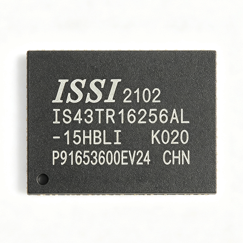
IS43TR16256A-15HBL-TR - 4Gb DDR3 SDRAM 667MHz | ISSI
The IS43TR16256A-15HBL-TR is a 4Gbit DDR3 SDRAM organized as 256M x 16, operating at a clock frequency of 667 MHz (data rate 1333 Mbps) with a CAS latency of 20 ns. It is housed in a 96-ball TWBGA (9x13 mm) package and operates from a 1.5V power supply. This memory IC is designed for high-bandwidth applications requiring reliable, high-speed data storage and retrieval. DDR3 SDRAM (Double Data Rate Type 3 Synchronous Dynamic Random-Access Memory) is a type of synchronous dynamic random-access memory with a high bandwidth interface, double the data rate of DDR2. It achieves higher transfer rates by transferring data on both edges of the clock signal, effectively doubling the data rate without increasing the clock frequency. DDR3 is part of the SDRAM family, which includes DDR, DDR2, DDR4, and DDR5, and is widely used in computing, networking, and embedded systems. Key features include a 4Gbit density, 16-bit I/O organization, 667 MHz clock speed, and a 20 ns CAS latency. The device supports programmable CAS latency, burst lengths of 8 and 4 (with burst chop), and on-die termination (ODT) for improved signal integrity. It also features auto-refresh and self-refresh modes for power saving, and a temperature-compensated self-refresh (TCSR) option. The IS43TR16256A-15HBL-TR utilizes a high-performance CMOS process and a bank architecture with 8 internal banks, enabling efficient interleaving and high throughput. The device includes DLL (Delay-Locked Loop) for precise timing alignment and supports write leveling and read leveling for system timing calibration. Its low power consumption and high speed make it suitable for a wide range of applications. Typical applications include networking equipment (routers, switches), industrial computing, embedded systems, and consumer electronics such as set-top boxes and smart TVs. The 1.5V operation and 96-ball TWBGA package allow for compact PCB designs with good thermal performance. When designing with this device, ensure proper decoupling capacitors near the power pins and follow the layout guidelines in the datasheet to minimize signal integrity issues. The device requires a stable 1.5V supply and a reference voltage (VREF) for the I/O.
IS43TR16256AL-107MBL - 4Gb DDR3L SDRAM 256Mx16 | ISSI
The IS43TR16256AL-107MBL is a 4Gb DDR3L SDRAM organized as 256Mx16, operating at 1.35V with a data rate of 1866MT/s. It is housed in a 96-ball TWBGA (9x13mm) package, offering high density and low power consumption for a wide range of computing and embedded applications. DDR3L (Low Voltage DDR3) is a type of synchronous dynamic random-access memory that operates at 1.35V, reducing power consumption by about 15% compared to standard 1.5V DDR3. It is part of the DDR3 SDRAM family, which uses double data rate architecture to transfer data on both edges of the clock, achieving high bandwidth. DDR3L is commonly used in mobile devices, networking equipment, and industrial computing where power efficiency is critical. Key features include a parallel interface with 933 MHz clock speed, 20 ns access time, and support for 1866MT/s data rate. The device supports various burst lengths (8 and 4 with burst chop), on-die termination (ODT), and programmable CAS latency. It operates over a temperature range of 0°C to +95°C (case) and is RoHS compliant. The IS43TR16256AL-107MBL utilizes advanced DRAM process technology, providing high reliability and performance. It features auto-refresh and self-refresh modes, which are essential for low-power standby operation. The 96-ball TWBGA package ensures excellent thermal and electrical performance, making it suitable for space-constrained designs. Typical applications include networking routers and switches, enterprise storage systems, industrial PCs, and embedded computing platforms. Its low voltage and high density make it ideal for memory-intensive applications where power efficiency is a priority. When designing with this device, ensure proper decoupling capacitors are placed near the power pins to minimize noise. The DDR3L interface requires careful PCB layout to maintain signal integrity at high speeds, including matched trace lengths and controlled impedance.
IS43TR16256AL-107MBLI - 4Gb DDR3L SDRAM 256Mx16 | ISSI
The IS43TR16256AL-107MBLI is a 4Gb DDR3L SDRAM organized as 256M x 16 bits, operating at a clock speed of 933 MHz (data rate 1866 Mbps) with a supply voltage of 1.35V. It is housed in a 96-ball TWBGA (9x13mm) package, making it suitable for high-density memory applications in computing, networking, and industrial systems. DDR3L SDRAM (Double Data Rate 3 Low Voltage) is a type of synchronous dynamic random-access memory that operates at a lower voltage (1.35V) compared to standard DDR3 (1.5V), reducing power consumption by up to 20% while maintaining backward compatibility with 1.5V operation. It is part of the DDR3 memory family, which uses double data rate signaling to transfer data on both edges of the clock, achieving high bandwidth for demanding applications. Key features include a 16-bit I/O interface, 4Gbit density, 20ns access time, and support for 1.35V operation with backward compatibility to 1.5V. The device offers high-speed data transfer rates, low power consumption, and is RoHS compliant. The 96-ball TWBGA package provides a compact footprint suitable for space-constrained designs. Technically, the IS43TR16256AL-107MBLI utilizes a 4-bank architecture with 8 internal banks, supporting burst lengths of 8 and 4, and features on-die termination (ODT) for improved signal integrity. It includes programmable CAS latency, additive latency, and write latency, allowing system designers to optimize timing for their specific memory controller. The device also supports auto-refresh and self-refresh modes for power saving. Typical applications include servers, networking equipment, industrial PCs, and embedded systems where high memory density and low power are critical. The 1.35V operation makes it ideal for power-sensitive designs, while the 1866 Mbps data rate supports high-bandwidth workloads. When designing with this device, ensure proper decoupling capacitors near the power pins and follow the layout guidelines in the datasheet to minimize signal integrity issues. The device requires a stable 1.35V supply and careful attention to termination for the address/control and data lines.
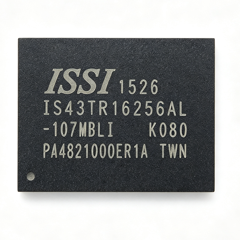
IS43TR16256AL-107MBLI-TR - 4Gb DDR3L SDRAM 256Mx16 | ISSI
The IS43TR16256AL-107MBLI-TR is a 4Gb DDR3L SDRAM organized as 256Mx16, operating at 1.35V with a data rate of 1866 Mbps (933 MHz clock). It is housed in a 96-ball TWBGA (9x13mm) package and is designed for low-power applications requiring high memory density. This device is backward compatible with 1.5V DDR3, allowing flexible system design. DDR3L SDRAM is a type of double data rate synchronous dynamic random-access memory that operates at a lower voltage (1.35V) compared to standard DDR3 (1.5V), reducing power consumption by about 20%. It is part of the memory hierarchy in computing systems, serving as main memory for processors, and is widely used in servers, networking equipment, and embedded systems where power efficiency is critical. Key features include a parallel interface with 16-bit data bus, 20ns access time, and support for on-die termination (ODT) and DLL-off mode for power saving. The device supports burst lengths of 8 and 4, and includes programmable CAS latency and additive latency. It operates over a temperature range of 0°C to +95°C (case temperature) for standard operation. The IS43TR16256AL-107MBLI-TR utilizes advanced DRAM process technology to achieve high density and low power. It features auto-refresh and self-refresh modes, with a typical self-refresh current of [DATA_NEEDED: self-refresh current]. The device includes a mode register set (MRS) for configuration, and supports write leveling and read leveling for signal integrity in high-speed systems. Typical applications include servers, networking equipment, industrial computing, and embedded systems where high memory density and low power are required. The 1.35V operation makes it ideal for battery-powered devices and energy-efficient data centers. When designing with this device, ensure proper decoupling capacitors near the power pins and follow the PCB layout guidelines in the datasheet to maintain signal integrity at 1866 Mbps. The device requires a stable 1.35V supply and a separate VDDQ supply for the I/O.
IS43TR16256AL-125KBL - 4Gb DDR3L SDRAM 256Mx16 | ISSI
The IS43TR16256AL-125KBL is a 4Gbit DDR3L SDRAM organized as 256M x 16, operating from a 1.35V supply with backward compatibility to 1.5V. It is housed in a 96-ball TWBGA (9x13mm) package and supports data rates up to 1600Mbps (800 MHz clock). This memory IC is designed for high-performance computing, networking, and embedded systems requiring low power and high bandwidth. DDR3L (Double Data Rate 3 Low Voltage) is a type of synchronous dynamic random-access memory (SDRAM) that operates at a lower voltage (1.35V) compared to standard DDR3 (1.5V), reducing power consumption by about 20-30% while maintaining similar performance. It is part of the DDR3 family, which uses double data rate signaling to transfer data on both edges of the clock, and is widely used in laptops, servers, and industrial applications where energy efficiency is critical. Key features include a parallel interface with 16-bit data bus, 800 MHz clock frequency, 20 ns access time, and support for 1.35V operation. The device is RoHS compliant and lead-free, making it suitable for environmentally conscious designs. The 96-TWBGA package offers a compact footprint with a 9x13mm body, ideal for space-constrained PCB layouts. Technically, the IS43TR16256AL-125KBL uses a high-density DRAM process, achieving 4Gbit capacity in a single package. It supports standard DDR3L features such as on-die termination (ODT), programmable CAS latency, and burst lengths of 8. The low voltage operation reduces I/O power, while the 20ns access time ensures fast random access for demanding applications. Typical applications include embedded computing, networking equipment (routers, switches), industrial automation, and automotive infotainment systems. Its low power and high density make it ideal for memory-intensive tasks in portable and battery-powered devices. When designing with this component, ensure proper decoupling capacitors near the power pins and follow the layout guidelines in the datasheet to minimize signal integrity issues at high speeds. The 1.35V supply must be regulated accurately to maintain reliable operation.
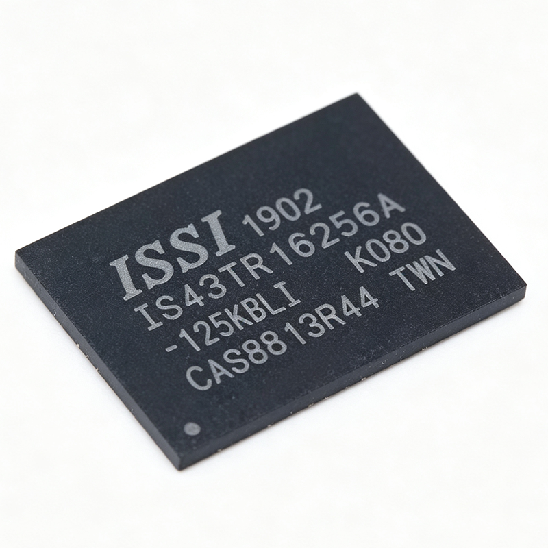
IS43TR16256AL-125KBLI-TR - 4Gbit DDR3L SDRAM 256Mx16 | ISSI
The IS43TR16256AL-125KBLI-TR is a 4Gbit DDR3L SDRAM organized as 256M x 16, operating at a clock frequency of 800 MHz (data rate 1600 Mbps) with a CAS latency of 11. It is supplied in a 96-ball TWBGA (9x13 mm) package and is designed for low-voltage operation at VDD and VDDQ = 1.35V, with backward compatibility to 1.5V. This memory IC is part of ISSI's DDR3L family, offering high density and bandwidth for a wide range of applications. DDR3L (Double Data Rate 3 Low Voltage) SDRAM is a type of synchronous dynamic random-access memory that transfers data on both edges of the clock signal, effectively doubling the data rate. The 'L' designation indicates low-voltage operation at 1.35V, reducing power consumption by about 20% compared to standard DDR3 at 1.5V. DDR3L is widely used in mobile devices, embedded systems, and industrial computing where power efficiency is critical. It is backward compatible with 1.5V DDR3, allowing flexible system design. Key features include a 4Gbit density, 16-bit data bus, 800 MHz clock speed, and a burst length of 8. The device supports on-die termination (ODT), programmable CAS latency, and auto-refresh and self-refresh modes. It operates over a temperature range of -40°C to +95°C (TC), making it suitable for industrial environments. The 96-ball TWBGA package provides a compact footprint with excellent thermal and electrical performance. Technically, the IS43TR16256AL-125KBLI-TR uses a 1.35V power supply for both core and I/O, reducing power dissipation. It features a 20ns row cycle time (tRC) and a 20ns row active time (tRAS). The device supports a data transfer rate of 1600 Mbps per pin, delivering high bandwidth for memory-intensive applications. The low-voltage operation and industrial temperature range make it ideal for embedded systems that require reliable performance in harsh conditions. Typical applications include industrial automation, networking equipment, embedded computing, and automotive infotainment systems. The 4Gbit density and x16 organization are well-suited for applications requiring moderate memory capacity with a wide data bus. The low-voltage operation helps extend battery life in portable devices and reduces thermal load in dense systems. When designing with this component, ensure proper decoupling capacitors are placed near the power pins to minimize noise. The DDR3L interface requires careful PCB layout to maintain signal integrity at 1600 Mbps. Refer to the ISSI datasheet for detailed timing parameters and layout guidelines.
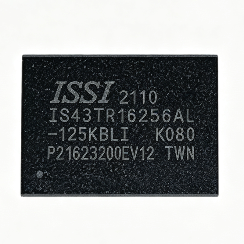
IS46TR16256A-125KBLA2 - 4Gb DDR3 SDRAM 256Mx16 | ISSI
The IS46TR16256A-125KBLA2 is a 4Gb DDR3 SDRAM organized as 256Mx16, operating at 1.5V with a data rate of 1600MT/s (800 MHz clock). It is housed in a 96-ball TWBGA (9x13mm) package, offering high-density memory for computing, networking, and industrial applications. This device supports 8 internal banks for concurrent operation and features programmable CAS latency, burst length, and on-die termination (ODT) for signal integrity. DDR3 SDRAM (Double Data Rate Type 3 Synchronous Dynamic Random-Access Memory) is a type of synchronous dynamic random-access memory with a high bandwidth interface, transferring data on both rising and falling edges of the clock. It is the successor to DDR2 and offers higher speeds and lower power consumption, making it a standard choice for main memory in computers, servers, and embedded systems. DDR3 operates at 1.5V, reducing power compared to DDR2's 1.8V, and supports data rates from 800 to 2133 MT/s. Key features include a 20ns tRCD (RAS-to-CAS delay), 290mA operating current, and a temperature range of 0°C to +95°C (Tc). The device is RoHS compliant and supports both standard and low-voltage (1.35V) operation, providing flexibility in power-sensitive designs. The 96-ball TWBGA package with a 9x13mm footprint enables compact PCB layouts, and the 256Mx16 organization simplifies bus design by reducing the number of devices needed for wide data paths. Architecturally, the IS46TR16256A-125KBLA2 uses an 8-bank design with a 16-bit I/O interface, achieving a peak bandwidth of 12.8 GB/s per device. It incorporates DLL (Delay-Locked Loop) for precise clock alignment, and supports programmable read and write latencies. The device also features auto-refresh and self-refresh modes for power management, and on-die termination (ODT) to improve signal quality on high-speed buses. Typical applications include main memory for embedded processors, networking equipment (routers, switches), industrial PCs, and high-performance computing modules. Its high density and speed make it suitable for applications requiring large memory footprints, such as video processing, data acquisition, and telecommunications infrastructure. When designing with this DDR3 device, ensure proper termination and layout for high-speed signals, and follow the JEDEC DDR3 guidelines for power supply decoupling and signal integrity. The device requires a 1.5V supply for VDD and VDDQ, and a separate VREF for address/command signals.
IT:A - 1Gbit NAND Flash Memory | Micron | Embedded Storage
The Micron IT:A is a 1Gbit (128MB) NAND Flash memory device organized as 128M x 8 bits, designed for high-density non-volatile storage in embedded systems. It operates from a 3.3V supply and uses a standard parallel NAND interface with a multiplexed address/data bus. The device is available in a 48-pin TSOP package, making it suitable for a wide range of consumer and industrial applications. NAND Flash memory is a type of non-volatile storage that retains data without power, using floating-gate transistors to store charge. It is the dominant technology for mass storage in portable devices, memory cards, and solid-state drives. NAND is organized into blocks and pages, with data written in page-sized increments and erased in block-sized increments, offering high density at low cost compared to NOR Flash. Key features include a page size of 2048 bytes with 64 bytes of spare area, a block size of 128KB, and a read access time of 25 microseconds. The device supports a program/erase cycle endurance of 100,000 cycles and has a data retention of 10 years. It includes an on-chip write controller that manages the programming and erasing algorithms automatically, simplifying system integration. The IT:A uses a standard NAND command set, including commands for read, program, erase, and status read. It features a ready/busy pin for status monitoring and supports both sequential and random access patterns. The device is designed for high-reliability applications, with error correction code (ECC) support recommended for data integrity. Typical applications include solid-state drives, embedded storage in industrial control systems, set-top boxes, and portable consumer electronics. The high density and low cost per bit make it ideal for boot code storage, data logging, and file system implementation in embedded designs. When designing with this device, ensure proper decoupling on the power supply and follow the recommended layout for the TSOP package. The write-protect pin should be tied to a known state to prevent accidental writes during power-up. ECC is strongly recommended to handle bit errors that occur over the device's lifetime.
K3K8K80BM-JGCT - Samsung LPDDR DRAM Memory IC | Samsung Electronics
The Samsung Electronics K3K8K80BM-JGCT is a mobile DRAM memory IC from Samsung's K3K series of low-power SDRAM components, supplied in a ball grid array (BGA) package for space-constrained mobile and embedded designs. Samsung's K3K part-number prefix designates its LPDDR (Low Power Double Data Rate) DRAM component family used in smartphones, tablets, and embedded computing platforms. Low-power DDR DRAM is a class of volatile memory that transfers data on both edges of the clock to double bandwidth while reducing operating and standby power. Within the memory hierarchy, LPDDR sits below DDR5 server DIMMs in raw bandwidth but dominates mobile and battery-powered systems because of its low core voltage, deep power-down modes, and PoP (Package-on-Package) or discrete BGA mounting options. It is a direct child of the broader SDRAM/DRAM semiconductor category. Key characteristics of this device class include high-speed bidirectional data transfer, per-bank and per-rank power management, dynamic voltage and frequency scaling, and initialization/training sequences defined by the JEDEC LPDDR specification in force for the die generation. Samsung mass-produces these dies on advanced DRAM process nodes with stacked or planar cell arrays. Architecturally, Samsung LPDDR components integrate the memory array, sense amplifiers, row/column decoders, DLL/phase-alignment circuitry, and I/O gating on a single die, with the package ball map exposing the CA (command/address) bus and DQ data lanes. Typical applications include smartphone application-processor memory, tablet and notebook SoC main memory, automotive infotainment memory subsystems, and embedded AI/edge-computing modules that require high bandwidth per watt. A key design consideration is signal integrity: LPDDR CA/DQ routing requires length-matched, impedance-controlled traces and careful fly-by or daisy-chain topology, and controller training must match the Samsung die's datasheet timing parameters. This page synthesizes verified distributor data, same-family alternative MPNs, and practical design notes not found in the manufacturer datasheet.
K3K9K90BM-MGCP - LPDDR5 DRAM | Samsung Semiconductor
The Samsung K3K9K90BM-MGCP is an LPDDR5 (Low Power Double Data Rate 5) DRAM memory integrated circuit from Samsung Semiconductor, supplied in a PBGA (Plastic Ball Grid Array) package. Samsung's LPDDR5 family delivers pin speeds of up to 6400 Mbps and aggregate bandwidth of up to 51.2 GB/s per device, with approximately 20% lower power consumption than the previous LPDDR4X generation. LPDDR5 DRAM is a type of synchronous dynamic random-access memory optimized for low power and high bandwidth in mobile, edge computing, and embedded systems. In the memory hierarchy it sits under the DRAM -> synchronous DRAM -> low-power SDRAM taxonomy defined around the JEDEC LPDDR5 standard, and it succeeds LPDDR4X in mobile SoC memory subsystems. Key features of Samsung LPDDR5 devices include 6400 Mbps pin speed, deep power-down and per-bank refresh architectures that cut idle power, and a simplified two-channel architecture that improves command efficiency versus LPDDR4X. Density options across the K3K/K3L family range from 32 Gbit to 64 Gbit per package, organized as x32-wide interfaces for SoC attachment. Technically, LPDDR5 introduces WCK (word clock) strobing, bank group architecture, and DVFS (dynamic voltage frequency scaling) of the clock domain, allowing the memory controller to throttle speed and voltage to match workload, which is the main source of the ~20% system power saving versus LPDDR4X. Typical applications include flagship smartphone and tablet main memory, AI edge accelerators, automotive infotainment and ADAS platforms, and 5G networking equipment where high bandwidth per watt is critical. Design consideration: LPDDR5 signal integrity requires tightly matched length routing of CA, DQ, DQS, and WCK traces on the PCB; consult the Samsung LPDDR5 design guide for fly-by topology and termination recommendations. This page synthesizes distributor stock data, drop-in same-family alternatives, and practical design notes not found in the manufacturer datasheet.
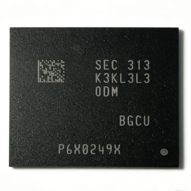
K3KL3L30DM-BGCU - LPDDR5X 64Gb 8533Mbps DRAM | Samsung
The Samsung Semiconductor K3KL3L30DM-BGCU is a 64 Gb LPDDR5X low-power DRAM memory IC operating at 8533 Mbps data rate, organized x64, in a 496-ball FBGA package. It operates from multiple supply rails of 1.8 V, 1.05 V, 0.9 V and 0.5 V and is rated for -25 C to +85 C operation. LPDDR (Low Power Double Data Rate) SDRAM is a type of synchronous dynamic random-access memory optimized for mobile and power-sensitive systems. Within the memory hierarchy, LPDDR5X sits at the top of the JEDEC low-power DRAM family (LPDDR4 -> LPDDR5 -> LPDDR5X), functioning as the main-system memory IC that feeds CPUs, GPUs and NPUs in smartphones, tablets, automotive computing platforms and AI edge devices. Key features of the K3KL3L30DM-BGCU include its 8533 Mbps pin speed, which places it in the highest LPDDR5X speed bin, and its 64 Gb density per device, enabling multi-gigabyte system memory with only a few ICs. The x64 organization and 496-ball FBGA footprint allow dense PCB routing on mobile-style boards. Technically, LPDDR5X extends LPDDR5 with higher signaling rates and improved power efficiency. Samsung states its LPDDR5X family delivers up to 8.5 Gbps data processing speeds with approximately 20% better power efficiency than LPDDR5, making it suited to AI inference, high-resolution imaging pipelines and 5G data throughput. Typical applications include flagship smartphone main memory, automotive infotainment and ADAS compute modules, AI edge accelerators, and premium tablet and laptop DRAM subsystems paired with Qualcomm or MediaTek application processors. A key design consideration is power-integrity: LPDDR5X at 8533 Mbps demands tight rail regulation on the 0.5 V VDDQ domain, careful fly-by trace length matching and per-rail decoupling per the memory controller vendor layout guide. This page consolidates distributor stock signals, family cross-references and practical sourcing notes beyond the bare datasheet listing. Pricing is RFQ-based as of 2026-09-04 because this EOL-status part trades through broker channels rather than fixed catalog tiers.
K3KL3L30QM-JGCT - LPDDR5X 64Gb 7500Mbps DRAM | Samsung
The Samsung K3KL3L30QM-JGCT is a 64 Gb LPDDR5X DRAM memory IC organized x64, supporting data rates up to 7500 Mbps per pin, supplied in a fine-pitch ball grid array (FBGA) package for mobile and edge computing platforms. LPDDR5X (Low Power Double Data Rate 5X, per the JEDEC LPDDR5X standard family) is an extension of LPDDR5 that raises signaling speed and improves power efficiency for battery-operated and thermally constrained systems. In the memory hierarchy it sits as volatile main-system DRAM below persistent storage such as NAND flash and eMMC, providing the working memory bandwidth that CPUs, GPUs, and NPUs require. Key features of the K3KL3L30QM-JGCT include its 64 Gbit density (8 GB equivalent per device), x64 organization for wide memory buses, and 7500 Mbps/pin data rate, which places it in the LPDDR5X performance tier used by flagship smartphones, tablets, AI edge accelerators, and automotive infotainment SoCs. As a Samsung third-generation 10nm-class DRAM product line part, it delivers higher bandwidth than LPDDR5 at lower power per transferred bit. Technically, LPDDR5X operates with a low-voltage I/O rail (VDDQ around 0.3-0.5 V class, per Samsung LPDDR5X documentation) and uses advanced training, on-die termination, and link ECC-style features inherited from LPDDR5 to maintain signal integrity at multi-gigabit speeds. Ball-grid-array interconnects minimize parasitic inductance, enabling clean eye diagrams at 7500 Mbps when the PCB stackup follows Samsung's package-on-package and fly-by routing guidance. Typical applications include flagship smartphone and tablet main memory, AI accelerator and NPU buffer memory, automotive domain-controller DRAM, and high-performance embedded and edge-server modules such as LPDDR5X SODIMMs and memory-down designs. Design consideration: LPDDR5X signal integrity is highly layout sensitive - length-matched, reference-plane-continuous routing and strict power-integrity budgeting for VDDQ are mandatory; insufficient decoupling at 7500 Mbps manifests as training failures rather than gradual degradation. This page adds value beyond the datasheet by synthesizing distributor stock levels, drop-in family alternatives, and practical design notes in one place.
K3KL5L50DM-BGCU - LPDDR5X 128Gb 8533Mbps DRAM | Samsung
The Samsung Semiconductor K3KL5L50DM-BGCU is a premium low-power DRAM (LPDDR5X) memory IC offering 128 Gb (16 GB) of density and an 8533 Mbps data rate per pin, packaged in a fine-pitch ball grid array (496-ball FBGA per distributor listings). It belongs to Samsung's LPDDR5X family, which delivers up to 8.5 Gbps pin speeds and approximately 20% better power efficiency than LPDDR5 at comparable speeds. LPDDR5X (Low Power Double Data Rate 5X) is an JEDEC-defined evolutionary step of the LPDDR5 SDRAM standard, aimed at mobile, automotive, and edge-AI computing systems. In the memory hierarchy, DRAM sits as the main system memory between the processor and non-volatile storage, providing high-bandwidth working memory; LPDDR variants optimize this role for battery-powered and thermally constrained devices by lowering I/O and core voltages and adding deep power-down states. Key characteristics of this part include the 128 Gb monolithic density, the 8533 Mbps (8.5 Gbps) transfer rate per data pin, and the ultra-low-power architecture typical of Samsung's LPDDR5X portfolio, which supports dynamic voltage scaling and advanced sleep modes. The high pin speed translates directly into memory bandwidth critical for large-language-model inference, 5G modems, and high-resolution imaging pipelines. Technically, LPDDR5X devices use bank group architectures with 16n prefetch, on-die termination, and command/address training to sustain multi-gigabit signaling. Samsung's premium LPDDR5X line further emphasizes power efficiency through enhanced ECC features and refined process nodes, allowing smartphone SoCs and automotive ADAS platforms to exploit full bandwidth within tight thermal envelopes. Typical applications include flagship smartphone and tablet main memory (often stacked as multi-die packages), AI accelerator companion memory in edge servers, automotive infotainment and ADAS domains, and high-performance embedded modules. A key design consideration: LPDDR5X signal integrity at 8.5 Gbps demands strict fly-by topology routing, length-matched traces, and SoC memory-controller training support; dropping to an LPDDR5-only controller limits operation to 6400 Mbps class speeds. This page synthesizes distributor stock data (16,750 pcs reported as of Aug 31, 2026), same-family alternatives, and practical design notes not found in the manufacturer datasheet.
K3KL5L50QM-JGCT - 128Gb LPDDR5X 7500Mbps DRAM | Samsung
The Samsung K3KL5L50QM-JGCT is a 128 Gb (16 GB) LPDDR5X low-power DRAM memory IC delivering data rates up to 7500 Mbps per pin with a x64 organization, housed in a 441-ball FBGA package operating from -25C to +85C across 1.8 V, 1.05 V, 0.9 V and 0.5 V supply domains. LPDDR5X (Low Power Double Data Rate 5X eXtended) is an enhanced evolution of the LPDDR5 DRAM standard defined by JEDEC. As a class of volatile DRAM within the broader memory hierarchy (LPDDR5X -> LPDDR family -> DRAM -> semiconductor memory), it prioritizes bandwidth-per-watt for battery-powered and thermally constrained compute platforms. Compared with LPDDR5, LPDDR5X raises interface speed and improves power efficiency, making it the dominant main-memory technology for flagship smartphones, tablets, and increasingly for AI accelerators and automotive computing. Key features of the K3KL5L50QM-JGCT include its 128 Gb monolithic density in a compact 441-ball FBGA footprint, 7500 Mbps (LPDDR5X-7500) interface speed, x64 channel organization suitable for 16-bit channel stacking, and an industrial-extended -25C to +85C operating range. Samsung reports that its premium LPDDR5X generation delivers up to 1.25 times the speed and roughly 25% better power efficiency versus the previous generation. Technically, the device uses Samsung advanced DRAM process technology with a multi-rail power architecture: VDD1 (1.8 V), VDD2 (1.05 V), VDDQ (0.5 V) and VDDCA/other aux rails, minimizing I/O switching power at multi-gigabit rates. The x64 organization allows SoC memory controllers to aggregate two 32-bit channels for full-bandwidth LPDDR5X operation. Typical applications include flagship smartphone and tablet main memory, AI edge computing and inference accelerators, in-vehicle infotainment and ADAS compute modules, and high-performance ultra-thin PCs. Design consideration: because this part is a ball-grid array memory, signal integrity on the command/address and data buses is critical; follow the SoC vendor reference layout for fly-by routing, ODT settings, and power rail sequencing. This page synthesizes distributor stock, drop-in family alternatives, and practical design notes not found in the manufacturer datasheet.
K3KL7L70EM-MGCU - 12Gb LPDDR5X DRAM, 315-Ball FBGA | Samsung
The Samsung K3KL7L70EM-MGCU is a 12 Gigabit (12 Gb) LPDDR5X low-power synchronous DRAM memory chip from Samsung Semiconductor, supplied in a 315-ball FBGA (Fine-Pitch Ball Grid Array) surface-mount package. This LPDDR5X DRAM is engineered for bandwidth-intensive, power-sensitive mobile and edge-computing platforms, operating at a data rate of up to approximately 8533 Mbps/pin as offered in Samsung's LPDDR5X family. LPDDR5X (Low Power Double Data Rate 5X eXtended) is an evolution of the LPDDR5 memory standard defined by JEDEC, pushing data rates and energy efficiency beyond conventional LPDDR5. In the memory hierarchy, DRAM sits between on-chip SRAM caches and non-volatile storage such as NAND flash, serving as the main working memory of a system-on-chip (SoC). LPDDR5X specifically targets flagship smartphones, tablets, AI edge accelerators, automotive infotainment, and high-performance portable devices that need more bandwidth than LPDDR5 at comparable or lower power. Key features of the K3KL7L70EM-MGCU include its 12 Gb single-die density, LPDDR5X-class speed grading (suffix -MGCU denotes speed and package options per Samsung part numbering), the compact 315-ball FBGA footprint, and Samsung's advanced low-voltage VDDQ operation that reduces I/O power versus LPDDR5. Samsung's LPDDR5X process technology supports deep power-down, per-bank refresh, and advanced bank-group architectures that improve effective bandwidth and standby efficiency. Architecturally, the device is organized as a x32-class LPDDR5X SDRAM with bank groups supporting burst-access scheduling. Command/address and data signals use Samsung LPDDR5X signaling with on-die termination (ODT) and link error checking options implemented per JEDEC LPDDR5X conventions, simplifying SoC PHY integration for Qualcomm Snapdragon and MediaTek Dimensity class platforms. Typical applications include flagship smartphone main memory, AI inference accelerators at the edge, automotive cockpit and ADAS domain controllers, and ultra-thin tablets or laptops using stacked/package-on-package memory configurations. When designing this device in, ensure the SoC memory controller explicitly supports LPDDR5X timing and speed-bin compatibility, and follow Samsung's layout guidelines for fly-by routing of CA/CLK nets and matched-length DQ/DBI/DQS groups. This page consolidates verified distributor listings, drop-in family alternatives, and practical design guidance not found in a single manufacturer datasheet.
K3KL9L90CM-MGCT - 64Gb LPDDR5X 7500Mbps x32 DRAM | Samsung
The Samsung K3KL9L90CM-MGCT is a 64 Gbit LPDDR5X SDRAM with a x32 memory organization and a maximum data rate of 7500 Mbps, housed in a 315-ball FBGA (BGA-315) package. LPDDR5X (Low Power Double Data Rate 5X) is an enhanced evolution of the LPDDR5 standard defined by JEDEC, targeting dramatically higher bandwidth with lower operating voltage. It sits at the top of the mobile DRAM hierarchy (LPDDR4X -> LPDDR5 -> LPDDR5X) and serves as the main-system-memory technology for smartphones, tablets, laptops, AI accelerators, and automotive infotainment platforms. As volatile memory, it provides fast working storage for a processor but must be re-initialized at every power cycle. Key features of this device include the 64 Gbit density per die (8 GByte per package in x32 organization), 7500 Mbps pin speed for approximately 300 Gbps of aggregate bandwidth per 32-bit channel, and LPDDR5X-class low supply voltages (VDDQ 500 mV core interface domain with 900 mV/1.05 V core rails and 1.8 V I/O and power domains per the JLCPCB listing). The industrial-grade operating range of -25C to +85C supports demanding embedded deployments. Architecturally, the device implements LPDDR5X signaling with dynamic voltage scaling, deep sleep modes, and per-bank refresh schemes inherited from LPDDR5, enabling platforms compliant with JEDEC JESD209-5B-class requirements to exploit full 7500 Mbps operation. Command/address training and DFE-based receiver equalization sustain signal integrity at high data rates over standard PCB stackups. Typical applications include AI edge-compute modules, high-performance smartphone and tablet main memory, industrial controllers requiring embedded logging, computing/COM express modules, and firmware boot and data-storage subsystems that pair DRAM with NAND. Design consideration: LPDDR5X at 7500 Mbps requires strict fly-by termination topology, length-matched routing, and careful power-domain isolation of the 500 mV VDDQ rail; memory-controller training quality directly determines achievable speed bin. This page consolidates verified distributor stock, drop-in same-family alternatives, and practical sourcing guidance not found in the manufacturer datasheet.
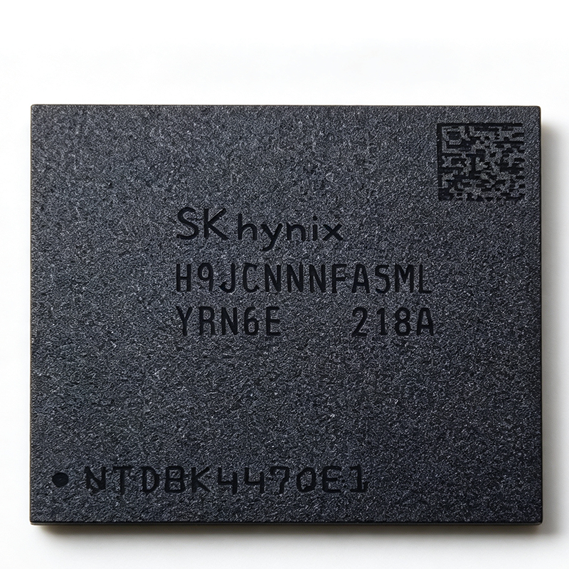
K3LKBKB0BM-MGCP - 32Gbit LPDDR5 DRAM 6400Mbps | Samsung
The Samsung K3LKBKB0BM-MGCP is a 32 Gbit LPDDR5 SDRAM memory IC with a 1G x32 organization and a data rate of 6400 Mbps, operating from 500 mV, 900 mV, 1.05 V and 1.8 V supply rails over an industrial-extended temperature range of -25C to +85C. The device is packaged in a fine-pitch FBGA ball grid array (data indicates FBGA-315, 1.05 V core class) and is RoHS compliant. LPDDR5 (Low Power Double Data Rate 5) is the fifth generation of JEDEC low-power synchronous DRAM, a class of volatile memory that stores working data for application processors and SoCs. Within the memory hierarchy, LPDDR5 sits under the broader DRAM family alongside DDR4/DDR5, but is optimized for bandwidth-per-watt in battery-powered and thermally constrained systems rather than raw module capacity. Key differentiating specifications include the 6400 Mbps/pin data rate, which doubles effective LPDDR4X-class bandwidth in comparable channel conditions; a 32 Gbit single-die density that allows 4 GB of memory in one package with a x32 I/O interface; and multi-rail operation (VDD1 1.05 V class core, VDD2 0.9 V class, VDDQ 0.5 V class, VDD2H 1.8 V class per the distributor listing) that reduces dynamic and standby power. The -25C to +85C operating window extends beyond the standard mobile range, supporting industrial controllers and outdoor connected devices. Technically, the device belongs to Samsung's LPDDR5 family, which uses deep-sleep states, bank-group architecture, and dynamic voltage frequency scaling to cut idle power dramatically versus LPDDR4. Speed-class grading (this part is listed alongside LPDDR5-5500/6400 class material in web listings) allows platform designers to match memory bandwidth to SoC controller capability. Signal integrity at 6400 Mbps requires careful length-matched routing and reference-plane discipline on the PCB. Typical applications include flagship smartphones and tablets, AI edge-compute modules, automotive infotainment SoCs, networking appliances, and industrial computing modules where 4 GB LPDDR5 density and low standby power are required. Design consideration: at 6400 Mbps, routing and power-delivery design dominate system margins; use fly-by topology guidance from the Samsung LPDDR5 datasheet and validate the design at the corner data rates during SI/PI sign-off. This page synthesizes distributor pricing, stock availability, drop-in alternative guidance, and practical design notes not found in the manufacturer datasheet alone.