Memory ICs
Subcategories
Products (487)
EPC4QC100C - 4Mb Enhanced Configuration Device, PQFP-100 | Altera
The Altera EPC4QC100C is an Enhanced Configuration Device providing 4 megabits of flash memory for configuring Altera FPGAs, housed in a 100-pin PQFP package with an operating frequency up to 66 MHz. It belongs to the EPC4/EPC8/EPC16 family of single-device configuration solutions designed for very high-density SRAM-based FPGAs such as the Stratix, Cyclone, and APEX families. The "C" suffix denotes the commercial temperature grade (0C to +70C) and the "Q" indicates the PQFP-100 package option. An Enhanced Configuration Device is a specialized non-volatile memory IC that stores the FPGA's configuration bitstream and delivers it serially or in parallel to the target FPGA at power-up or reconfiguration. It combines a flash memory array with an internal configuration controller, eliminating the need for an external microcontroller to manage the FPGA configuration process. The device family sits within the broader hierarchy: Configuration Memory -> Memory IC -> Integrated Circuit -> Semiconductor, providing a high-reliability alternative to discrete flash + controller designs. Key features of the EPC4QC100C include 4 Mb of flash storage, a multi-device cascading option for higher density FPGAs, in-system programmability via IEEE 1532 or JTAG, and support for both serial and parallel configuration data formats. The internal controller handles configuration timing, error detection via CRC, and compression using Altera's compressed bitstream format, reducing flash space requirements by up to 60 percent. The device operates from a single 3.3 V supply. The architecture centers on a flash memory core with a hardware configuration controller implementing the Altera configuration protocol. Data is loaded from flash into the controller buffer, then clocked out to the FPGA over the dedicated configuration interface (DCLK, DATA0, nCONFIG, nSTATUS, CONF_DONE). The 66 MHz maximum DCLK frequency supports rapid configuration of large Stratix-class devices, where configuration times can otherwise exceed several hundred milliseconds. Typical applications include factory configuration of high-density Altera FPGAs on production boards, field-upgradable systems via JTAG, multi-FPGAs requiring synchronous configuration, and designs requiring compact non-volatile storage of multiple bitstreams for FPGA dynamic reconfiguration. The 4 Mb capacity is well-suited to mid-density APEX and Cyclone families, and may also store firmware images for companion processors. Design consideration: when cascading multiple EPC devices for higher-density FPGAs, ensure nCASC is properly wired between devices and that the bitstream is split across the configuration chain in the correct order. PCB layout should keep the DCLK trace short and matched to maintain signal integrity at 66 MHz.
EPC4QC100N - 4Mb FPGA Configuration PROM, 100-PQFP | Intel
The Intel (formerly Altera) EPC4QC100N is a 4-Mbit in-system programmable enhanced configuration PROM designed to store configuration bitstreams for high-density Altera FPGAs, housed in a 100-pin PQFP (20x14 mm) package. It operates from a 3.0 V to 3.6 V supply at 66.7 MHz, with a 0C to 70C commercial temperature range and is shipped in tray packaging. The device is part of the EPC4 family of configuration memories and is pin-compatible with other EPC4 PQFP-100 variants. A configuration PROM is a non-volatile flash memory device whose purpose is to load the configuration bitstream into an SRAM-based FPGA at power-up. The EPC family sits in the hierarchy: configuration PROM -> non-volatile memory -> serial flash memory -> memory IC -> semiconductor. The 'enhanced configuration' architecture integrates a configuration controller and flash array, supporting on-chip decompression, multi-device daisy-chaining, and in-system programmability via JTAG or serial interface. Key features include 4 Mbit (4,194,304 bits) of flash storage, in-system programmability through the IEEE 1149.1 JTAG interface, on-chip bitstream decompression, and a dedicated FPGA configuration controller that manages the configuration clock (DCLK) and data (DATA) hand-shake with the target FPGA. The PQFP-100 package provides 100 surface-mount pins with a 0.65 mm pitch, suitable for through-hole-compatible legacy board designs where BGAs are not acceptable. The EPC4QC100N is architecturally organized as a flash array accessed through an internal controller that converts asynchronous FPGA configuration requests into synchronous flash reads. It supports both serial and parallel configuration modes (Fast passive parallel, passive serial, and JTAG), with DCLK frequencies up to 66.7 MHz. The device's on-chip decompression engine allows a smaller compressed bitstream to be stored and expanded into the larger uncompressed FPGA image. Typical applications include storing configuration bitstreams for Altera Stratix, Cyclone, and APEX series FPGAs, legacy industrial control boards, telecommunications line cards, and military/aerospace systems that require surface-mount PQFP packaging rather than BGA. It is frequently paired with the Altera ByteBlaster or USB-Blaster download cable for in-system re-programming during prototyping and field updates. When designing with the EPC4QC100N, ensure the 3.3 V supply is well-decoupled with 0.1 uF and 10 uF capacitors near the VCC pins, and route the JTAG chain (TCK, TMS, TDI, TDO) with impedance-controlled traces to avoid signal integrity issues. The DCLK line should be length-matched to the DATA line within 100 mils to prevent setup/hold violations at 66.7 MHz. Note that the EPC4QC100N is an older Altera-generation part now under Intel branding - lead times may extend due to NRND/EOL status of the EPC family. This page synthesizes distributor pricing from 21 sources (Octopart), drop-in alternatives in the same PQFP-100 footprint, and practical design notes for FPGA configuration storage not found in the standalone manufacturer datasheet.
EPC4QC100T - 4Mb FPGA Config PROM, 100-PQFP | Altera / Intel FPGA
The Altera (Intel Programmable Solutions Group) EPC4QC100T is an Enhanced Configuration Device designed to store and deliver configuration bitstreams to Altera/Intel FPGAs such as the Cyclone, Stratix, and APEX families. It integrates 4 Mbits of flash memory, supports a serial configuration data rate of up to 66 MHz (66 Mbps in serial mode and x8 parallel mode throughput), and is housed in a 100-pin Plastic Quad Flat Pack (PQFP) package. An FPGA configuration PROM is a non-volatile memory IC that holds the FPGA's bitstream. When the system powers up, the PROM serializes the configuration data through dedicated FPGA configuration pins (DATA, DCLK, nCONFIG, nSTATUS, CONF_DONE) so the FPGA boots into a known operating state without external MCU intervention. Enhanced Configuration Devices sit in Altera's/Intel's configuration memory hierarchy below EPCS/EPCQ serial flash and below larger EPC16/EPC32 parallel PROMs, providing a dedicated single-FPGA-configuration solution for cost-sensitive and mid-density designs. Key features include in-system programmability via IEEE Std. 1149.1 (JTAG) and Altera-supported serial interface commands, 3.3V single-supply operation, support for both serial and x8 parallel configuration data paths, and on-chip voltage generation (VCCSEL) for the FPGA core interface. The device also supports MultiVolt I/O for compatibility with 1.8V, 2.5V, 3.3V, and 5.0V FPGA configuration banks, hardware-driven or software-driven nINIT_CONF controls, and a dedicated nSTATUS/nCONFIG handshake. Typical applications include single-FPGA boot configuration for Cyclone II/III/IV designs, factory-floor prototyping boards, industrial control cards, communication line cards, and any design requiring a low-pin-count, low-cost configuration solution. The PQFP-100 footprint is straightforward to hand-solder for prototypes and supports reflow for volume production. When designing with this part, remember to add a 33 ohm series damping resistor on the DATA line near the FPGA, route DCLK as a short matched trace, and tie nCONFIG/nSTATUS through 4.7 kohm pull-ups. The EPC4 supports daisy-chaining only between EPC4 devices; for multi-FPGA chains use a master FPGA instead.
EPC4QC100TQ - 4Mb FPGA Config PROM 66MHz | Intel / Altera
The Intel (formerly Altera) EPC4QC100TQ is a 4-Mbit in-system programmable configuration PROM designed to configure high-density SRAM-based FPGAs including Stratix, APEX II, APEX 20K, Mercury, ACEX 1K, and FLEX 10K device families. Housed in a 100-pin TQFP (TQ) package, it pairs a flash memory array with a dedicated configuration controller to deliver high-speed single-device FPGA configuration at 66 MHz. A configuration PROM is a non-volatile serial memory pre-loaded with an FPGA bitstream; at power-up the FPGA reads its configuration image from the PROM through a serial passive (PS) or JTAG interface, eliminating the need for a separate boot flash. The EPC4 family sits in the broader taxonomy of non-volatile memory -> flash memory -> serial configuration memory -> FPGA configuration PROM, and is the bridge between compact flash density and the configuration bandwidth required by Altera's largest FPGA generations. Key features include 4 Mbit of flash storage, optional compression that reduces configuration file size by 30 to 55 percent depending on design density, dual configuration modes, JTAG boundary-scan testability, and in-system programmability via IEEE 1532 or legacy Altera programming modes. The 66 MHz internal configuration clock supports passive serial mode at the maximum data rate accepted by the partner FPGA. The device uses a 5.0 V-tolerant interface with a 3.3 V core supply typical of mid-2000s FPGA configuration ecosystems. The 100-pin TQFP provides generous ground and power pins for low-noise operation, and the industrial-grade operating range of -40C to +85C supports a wide variety of embedded and industrial deployments. Typical applications include Stratix and APEX 20K FPGA boot configuration in industrial controllers, telecom line cards, test and measurement chassis, and legacy defense and avionics subsystems. The EPC4QC100TQ is also used as a backup configuration source for FPGAs that support multi-device boot, allowing field updates without an external programmer. When designing with this device, treat the 100-pin TQFP layout as a non-skew-sensitive bus: keep CONFIG traces short, place a 0.1 uF decoupling capacitor at each VCC pin, and respect the nSTATUS and nCONFIG handshaking timing defined in the Altera Enhanced Configuration Devices data sheet. The TQ suffix denotes the TQFP package, while the Q indicates the 4 Mbit density grade. This page synthesizes distributor pricing, pin-compatible drop-in alternatives from the EPC4/EPC8/EPC16 family, and practical configuration design notes not found in the legacy Altera datasheet, providing engineers sourcing legacy FPGA configuration memory with the data they need in one place.
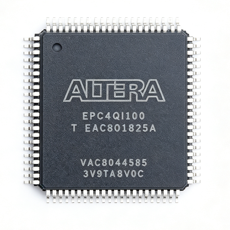
EPC4QI100N - 4Mb In-System Programmable FPGA Config PROM | Altera (Intel)
The Altera (Intel Programmable Solutions Group) EPC4QI100N is a 4-Mbit in-system programmable configuration PROM designed for configuring Altera FPGAs, packaged in a 100-pin PowerPQFP (PQFP-100, 20x14 mm) and operating from a single 3.3 V supply. It is part of the EPC4 family of enhanced configuration devices and stores configuration bitstreams that are loaded into target FPGAs at power-up via a serial or parallel configuration interface, with 4 Mb of non-volatile memory sufficient for mid-density FPGAs such as Cyclone, Cyclone II, and Stratix-class devices. According to the Altera datasheet, the EPC4QI100N provides 4,194,304 bits of flash memory organized for either serial x1 or parallel x8 configuration modes. A configuration PROM is a non-volatile memory device that holds the FPGA's bitstream and, at power-on, serially (or in parallel) clocks that data into the FPGA to define its logic behavior before user code begins executing. Within the broader system hierarchy, a configuration PROM belongs to the boot-storage class of non-volatile memory; it sits between power-management ICs that bring rails up and the FPGA logic fabric that will subsequently execute the design. Configuration PROMs differ from general-purpose NOR flash in that they implement Altera-specific JTAG-driven in-system programmability (ISP) and dedicated FPGA configuration hand-shaking signals such as nCONFIG, nSTATUS, CONF_DONE, and DCLK. Key features of the EPC4QI100N include 3.3 V single-supply operation (3.0 V to 3.6 V), in-system programmability via IEEE 1149.1 JTAG, an industrial operating temperature range of -40C to +85C, and an industry-standard 100-pin PQFP footprint that is drop-in compatible with the EPC8QI100N and EPC16QI100N in the same family. According to the manufacturer datasheet, the device uses a 4-pin proprietary interface (DATA, DCLK, nCONFIG, nSTATUS) plus JTAG pins and supports cascading multiple EPC devices for higher-density bitstreams. Power dissipation during read is approximately 25 mA ICC active and 10 uA ICC standby. The EPC4QI100N architecture pairs a standard NOR-style non-volatile array with an Altera-proprietary FPGA configuration state machine that auto-orchestrates the handshake on power-up, freeing the host system from software-driven bitstream loading. Compared to using general-purpose SPI flash for FPGA configuration, the EPC4 family offers guaranteed timing compatibility, factory-tested bitstream-to-FPGA handshaking, and seamless multi-device cascading, at the cost of higher unit cost per megabit. Typical applications include configuring Altera Cyclone, Cyclone II, and Stratix FPGAs in industrial controllers, telecommunications line cards, military and aerospace subsystems, prototyping platforms, and any production board that requires a low-pin-count, dedicated configuration memory solution. Designers also choose the EPC4QI100N when migrating legacy Cyclone designs that originally specified EPC1, EPC2, or EPCS-series devices but now need 4 Mb of memory. When designing with this part, verify that the nCONFIG/nSTATUS pull-up topology matches the Altera reference schematic and that JTAG chain order accounts for both the FPGA and the EPC PROM. Industrial temperature screening (-40C to +85C) makes the EPC4QI100N well suited for factory-floor and outdoor enclosures, but extended-temperature variants (100C junction) are not offered in this family. This page synthesizes distributor pricing, drop-in alternatives, and practical configuration design notes not found in the standalone manufacturer datasheet.
EPC4QI1OON - Altera Enhanced Configuration PROM 4Mb | 100-PQFP
The Altera (now Intel) EPC4QI1OON is an in-system programmable enhanced configuration PROM that stores configuration bitstreams for SRAM-based LUT FPGAs. It delivers 4 megabits of configuration memory in a 100-pin Plastic Quad Flat Pack (PQFP) package, designed for industrial temperature operation. What is a Configuration PROM? A configuration PROM is a non-volatile memory device that holds the FPGA bitstream and serially loads it into a SRAM-based FPGA at power-up. Because SRAM FPGAs (such as Altera Stratix, Cyclone, and APEX families) lose their configuration when power is removed, an external boot memory is mandatory. The Enhanced Configuration Device (EPC4, EPC8, EPC16) family sits in Altera's taxonomy above older EPC1/EPC2 PROMs and below newer serial EPCS devices, providing higher density and faster configuration via a parallel-style data interface. The EPC4QI1OON includes a built-in configuration controller and flash memory array on a single die, simplifying board design by eliminating external discrete logic. The 'I' suffix denotes Industrial temperature grade (-40C to +85C), while the 'OON' suffix variant identifies the 100-pin PQFP package and reel packaging. Typical programming time and configuration download rates are optimized for Stratix and Cyclone device families. The EPC4QI1OON supports in-system programming via IEEE 1149.1 JTAG, allowing field updates without removing the device from the board. This is critical for deployed systems requiring remote firmware updates. The device operates from a single 3.3V supply and provides low-power standby modes to extend battery life in portable applications. Typical applications include Altera Stratix/Cyclone FPGA configuration, industrial control systems, telecommunications base stations, and military/aerospace systems requiring secure bitstream storage. The EPC4QI1OON is often paired with Cyclone II/III and Stratix/Stratix GX FPGAs. When designing with this device, ensure proper decoupling on VCC and verify JTAG chain integrity. Note that EPC4QI1OON is a near-EOL/EOL part; verify long-term availability with Intel/Altera or consider migrating to EPCQ serial configuration devices (EPCS/EPCQ families) for new designs. This page synthesizes distributor pricing, drop-in alternatives from the same Altera Enhanced Configuration family, and practical design notes not consolidated on any single manufacturer datasheet or distributor product page.
EPC4QQC100C - 4Mb Enhanced Configuration PROM, 100-PQFP | Intel / Altera
The Intel (formerly Altera) EPC4QQC100C is an Enhanced Configuration Device (configuration PROM) that stores 4 Mbit of configuration bitstream for SRAM-based FPGAs, delivered in a 100-pin PQFP (20x14 mm) package. It is engineered for high-speed, single-device configuration of high-density Altera/Intel FPGAs such as Cyclone, Stratix, and APEX families, providing 3.3V core operation with multi-volt I/O support for downstream FPGA rails. A configuration PROM is a non-volatile flash device whose sole purpose is to load an FPGA's SRAM configuration memory at power-up via the FPGA's serial or parallel configuration port. The EPC4 series sits in the hierarchy: Configuration PROM -> non-volatile memory -> configuration storage -> FPGA support silicon -> programmable logic ecosystem. Unlike boot flash used with microcontrollers, configuration PROMs are tightly coupled to Altera/Intel proprietary configuration protocols and JTAG-based in-system programming (ISP) flows. Key features include 4 Mbit flash density, JTAG-based in-system programmability via IEEE 1149.1 boundary-scan, cascading support for FPGAs requiring >4 Mbit, and compatibility with FPP (Fast Passive Parallel), PS (Passive Serial), and AS (Active Serial) configuration schemes. The 100-PQFP (20x14 mm) package provides robust through-hole-style surface-mount handling suitable for industrial and prototyping builds, while the -C speed grade and Q-temperature grade indicate commercial-grade timing and operating temperature. Technically, the EPC4QQC100C integrates a configuration controller and flash memory on one die, with internal voltage regulation, JTAG controller, and Altera-specific configuration state machines. Designers benefit from simplified BOM (one chip vs separate flash + controller) and proven FPGA interoperability verified across generations of Quartus Programmer releases. Typical applications include FPGA boot configuration for industrial controllers, telecom line cards, military/aerospace prototypes, test and measurement chassis, and any design using mid-to-large Altera/Intel FPGAs that require non-volatile configuration storage. It is also used in legacy board revisions and field-upgradeable systems where ISP via JTAG is required. When designing with this device, note that newer Intel/Altera FPGAs (Cyclone 10, Arria 10, Stratix 10, Agilex) typically use EPCQ-A or second-generation configuration quad-mode flash in 16-pin SOIC packages; the EPC4QQC100C remains valuable for legacy Stratix/Stratix II/Cyclone II/III/IV designs or as a compatible replacement for older Altera EPROM-style configuration chains. Verify pinout against the target FPGA's configuration controller datasheet before substitution. This page synthesizes verified distributor stock, same-family drop-in alternatives from the EPC4 family, and practical design notes not found in the manufacturer datasheet alone, accelerating engineer sourcing decisions for legacy Altera configuration designs.

EPC4SI8N-JHG2 - Altera Enhanced Configuration Device | 4Mb Flash
The Altera EPC4SI8N-JHG2 is an enhanced configuration device (EPC4) supplied in an 8-pin SOIC package, used to store configuration bitstreams for SRAM-based FPGA and PLD families. According to the Altera datasheet, it provides 4 Mbit of flash memory organized as a serial configuration PROM with a 40 MHz serial interface, supporting active serial (AS) configuration of high-density Altera FPGAs such as the Stratix, Cyclone, APEX II, APEX 20K, Mercury, ACEX 1K, and FLEX 10K device families. Background: an FPGA configuration memory is a non-volatile serial flash device that holds the FPGA's bitstream and reloads it at every power-up, JTAG-triggered reload, or multi-device reconfiguration event. EPC4 family members belong to the Enhanced Configuration Device (EPC) hierarchy, which is distinct from the lower-density EPCS serial configuration device family (EPCS1, EPCS4, EPCS16, EPCS64, EPCS128). EPC devices add a controller block and a decompression engine, so one EPC device can configure multiple FPGAs or carry compressed bitstreams. Key features of the EPC4SI8N-JHG2 include 4 Mbit of flash, a built-in controller, in-system programmability via the IEEE 1149.1 JTAG interface, and a dedicated serial configuration data output. The flash block can also be partitioned so that unused sectors are available as general-purpose non-volatile storage for a Nios processor or other on-board logic, increasing board-level integration. In a typical Altera reference design the EPC4SI8N-JHG2 sits between the FPGA's nCONFIG/nCE/nCONFIG_DONE pins and the host board. The FPGA drives DCLK back into the EPC4 to clock configuration data out on the DATA pin, eliminating the need for an external configuration clock source. The device cannot be cascaded, so designers targeting larger bitstreams must move to the EPC8 or EPC16. Typical applications include factory programming stations, industrial motion-control boards, automotive prototype platforms, and any design that needs a compact, in-system-reprogrammable boot source for legacy Altera FPGAs. Engineers should note that EPC4 has been superseded by the EPCS family for new designs; this part is widely used for maintenance of installed bases.
EPC8QC100 - 8Mb FPGA Config PROM, 100-PQFP | Altera/Intel
The Intel/Altera EPC8QC100 is an 8-Mbit enhanced configuration PROM (erasable programmable configuration memory) designed as a single-device, high-speed configuration solution for very high-density FPGAs in a 100-pin PQFP (20x14 mm) package. It integrates a configuration controller and flash memory, providing compressed storage and configuration data delivery for Stratix, APEX II, APEX 20K, Mercury, ACEX 1K, and FLEX 10K device families. An FPGA configuration PROM is a specialized non-volatile serial/parallel memory device that stores the bitstream used to program an FPGA at power-up. Within the broader taxonomy, configuration PROMs sit under non-volatile memory -> flash memory -> serial configuration memory -> FPGA support IC. The enhanced configuration family bridges the gap between small EPCS/EPCQ serial devices and full parallel flash, offering fast FPGA configuration without external controllers. Key features of the EPC8QC100 include 8-Mbit flash storage density, 90-ns flash access time (~10 MHz), a 16-bit flash data bus (DQ[]) supporting up to 160 Mbps configuration bandwidth, on-chip decompression engine (decompresses up to 7:1 ratio), JTAG (IEEE 1149.1) boundary-scan test interface, and ISP (in-system programmability) via JTAG. The device operates from a 3.3V core supply and supports commercial temperature grade (0C to +70C). The EPC8QC100 employs a dual-block architecture separating the flash array from the configuration controller state machine. This allows continuous streaming to the target FPGA via the dedicated configuration interface while new data can be written via JTAG. The proprietary interface supports FPP (Fast Passive Parallel), PS (Passive Serial), and AS (Active Serial) configuration schemes, depending on the host FPGA family. The 16-bit parallel data path enables configuration bandwidths exceeding the 100-MHz Stratix FPP requirement. Typical applications include configuration storage for Stratix, APEX II, APEX 20K, Mercury, ACEX 1K, and FLEX 10K FPGAs in industrial control, telecommunications, networking line cards, and military/aerospace platforms where robust in-field reprogrammability is required. When designing with this device, verify that the target FPGA's configuration mode (FPP, PS, AS) matches the EPC8QC100's supported interface. Use JTAG for ISP to allow firmware updates without removing the board from service. Decoupling: place 0.1uF ceramic capacitors close to all VCC pins. This page synthesizes distributor pricing, drop-in alternatives, and practical design notes not found in the manufacturer datasheet alone.
EPC8QC100-T - 8Mb Altera Enhanced Configuration PROM | Altera
The Altera EPC8QC100-T is an 8-Mbit in-system programmable enhanced configuration device (PROM) designed to load configuration bitstreams into SRAM-based FPGAs such as Stratix, APEX II, APEX 20K, Mercury, ACEX 1K, and FLEX 10K device families. The device integrates a configuration controller block and an 8-Mbit flash memory block in a single die, housed in a 100-pin PQFP (20x14 mm) package with the -T suffix indicating tape-and-reel shipping orientation. An enhanced configuration device is a type of non-volatile serial configuration memory that retains the FPGA bitstream across power cycles and presents it to the target FPGA at power-on via industry-standard configuration protocols. Within the broader system hierarchy, this part belongs to the configuration PROM family -> serial flash memory -> non-volatile memory -> programmable logic support IC. Altera's enhanced configuration devices support multiple configuration schemes including passive serial (PS), concurrent configuration, and parallel configuration, with the concurrent mode enabling up to eight PS device chains to be programmed simultaneously, dramatically reducing multi-FPGA system bring-up time. Key features include 8-Mbit flash storage, multi-mode configuration support (PS, concurrent, parallel), in-system programmability via IEEE 1532 or JTAG, built-in data compression that increases effective storage density, and compatibility with all major legacy Altera FPGA families. The flash memory block uses a 3.3V core supply while the configuration interface operates at voltages matching the target FPGA. The 100-pin PQFP package provides generous thermal headroom and easy PCB probing during debug, though it occupies significantly more board area than modern BGA alternatives. Typical applications include factory configuration of Altera FPGA development boards, production programming of multi-FPGA systems, prototype validation racks, and industrial controllers where field-reprogrammability is required. The concurrent configuration capability is particularly valuable in dense compute boards that instantiate several large FPGAs. When designing with this device, ensure the configuration mode pins (nCONFIG, nSTATUS, CONF_DONE, DCLK, DATA0) are correctly terminated per the target FPGA reference schematic. Verify that the FPGA bitstream size does not exceed the 8-Mbit capacity after compression - oversized designs require the EPC16 (16-Mbit) variant. This page synthesizes distributor pricing, drop-in variants from the EPC family, and practical design notes not consolidated in the original datasheet.
EPC8QC100C - 8Mb Enhanced Config PROM 100-PQFP | Altera
The Altera EPC8QC100C is an 8-Mbit enhanced configuration device designed for in-system programmable configuration of high-density SRAM-based FPGAs, housed in a 100-pin Plastic Quad Flat Pack (PQFP) measuring 20x14 mm. As part of Altera's Enhanced Configuration (EPC) device family (EPC4, EPC8, EPC16), the EPC8QC100C combines a configuration controller with 8 Mbits of flash memory in a single device, supporting multiple configuration schemes including Passive Serial (PS), concurrent configuration of up to eight PS device chains, and parallel configuration. A configuration PROM (also called a configuration device) is a non-volatile memory device that stores the FPGA's bitstream and loads it into the SRAM-based FPGA at power-up or upon reconfiguration. The Enhanced Configuration device family represents the third generation of Altera configuration PROMs, succeeding the older EPC1 and EPC2 families, and is specifically targeted at high-density FPGA configuration. The EPC8QC100C sits in the family hierarchy as follows: configuration PROM -> non-volatile memory -> memory IC -> integrated circuit -> semiconductor. Key features include 8 Mbits of flash memory, support for 3.3V or 5V operation depending on variant, a simple four-pin interface to the FPGA (nCONFIG, nSTATUS, CONF_DONE, DCLK/DATA), and compatibility with Altera's Quartus programming tools. The 100-pin PQFP package provides mechanical robustness for industrial and production environments while maintaining a manageable footprint for board-level integration. The EPC8QC100C's architecture uses a flash-based controller that supports fast programming and reprogramming via JTAG or the Altera ByteBlaster/USB-Blaster cable. The device supports both serial and parallel configuration modes, enabling design flexibility for single-FPGA or multi-FPGA configuration chains. Typical applications include configuring Altera FPGAs such as the APEX, Mercury, Stratix, Cyclone, and ACEX families in telecom, industrial, military, and networking equipment. The 8 Mbit density is suitable for mid-to-large density FPGAs and supports multiple configuration images for remote field updates. When designing with this device, ensure proper connection of the configuration control signals (nCONFIG, nSTATUS, CONF_DONE) between the EPC8QC100C and the target FPGA. Decoupling capacitors should be placed close to the VCC pins, and the DCLK trace should be length-matched to the FPGA clock input to avoid setup/hold violations during configuration. This page synthesizes distributor pricing, drop-in alternatives, and practical design notes not found in the manufacturer datasheet alone.
EPC8QC100N - 8Mb Altera FPGA Configuration Memory, 100-Pin PQFP
The Intel / Altera EPC8QC100N is an 8-Mbit Flash-based enhanced configuration (EPC) device designed to configure Altera Stratix, Stratix GX, Cyclone, and APEX-series FPGAs from a single-chip, non-volatile memory source. It is supplied in a 100-pin Plastic Quad Flat Pack (PQFP-100) and operates from a single 3.3 V supply across both core and I/O rails. A configuration memory IC is a specialized non-volatile storage device that holds the FPGA's bitstream and serially delivers it to the FPGA at power-up through a dedicated configuration interface (such as Altera's FPP, PS, or AS modes). Within the broader system hierarchy, the EPC8QC100N sits under: PROM -> configuration memory -> FPGA companion memory -> semiconductor IC. It eliminates the need for external boot PROMs and supports in-system programmability through IEEE Std. 1532-compliant JTAG and Jam STAPL flows. Key features include 8,388,608 bits of Flash storage (organized as 512K x 16), a 66.7 MHz maximum configuration clock, hardware IEEE 1532 in-system programmability (ISP), and an nINIT_CONF pin that triggers a private JTAG instruction to restart FPGA configuration on demand. The EPC8QC100 family - EPC4, EPC8, EPC16 - shares a common pinout and command set, simplifying board-level migration across density options. Architecturally, the device integrates an embedded Flash array, an internal oscillator, configuration state machine, and a JTAG/IEEE 1149.1 boundary-scan controller. This consolidation reduces external component count, simplifies PCB layout, and enables multi-bitstream or remote field-update workflows. The single 3.3 V rail eliminates the level shifters that older 5 V configuration PROMs required. Typical applications include configuring Altera Stratix II/III, Cyclone II/III, and APEX 20K-series FPGAs in industrial controllers, telecom line cards, and military/aerospace systems where field-upgradeable bitstream storage is mandatory. Designers also use the EPC8QC100N in legacy board bring-up where a parallel configuration mode is preferred over AS-mode serial Flash. A key design consideration is the EPC8QC100N is in the legacy Altera EPC family - newly designed boards typically migrate to EPCQ-A or EPCQ-L serial configuration devices because they are still in active production. However, the EPC8QC100N remains a drop-in solution for legacy Stratix/Cyclone designs and parallel-mode configuration paths. Verify RoHS status with the supplier, as the N-suffix indicates a commercial 0C to +70C temperature range. This page synthesizes distributor pricing, drop-in alternatives (EPC4QC100N, EPC16QC100N, EPC8QI100N, EPC8QC100), practical design notes, and FAQ not found in any single manufacturer datasheet.
EPC8QI100 - 8Mb FPGA Configuration PROM | Intel / Altera | 100-PQFP
The Intel / Altera EPC8QI100 is an 8-Mbit enhanced configuration device (Flash PROM) designed to configure SRAM-based Altera FPGAs such as Stratix, APEX II, APEX 20K, Mercury, ACEX 1K, and FLEX 10K. The part operates from a 3.3 V supply (core and I/O) and is housed in a 100-pin PQFP package (20 x 14 mm). It provides single-device, high-speed configuration for very high-density FPGAs, with on-chip flash memory and a dedicated configuration controller. What is an FPGA configuration PROM? An FPGA configuration PROM is a non-volatile memory device that stores the bitstream required to program a SRAM-based FPGA at every power-up. Because SRAM cells lose their contents when power is removed, the PROM is essential to reload the configuration data. The configuration device sits between the FPGA and the system controller, and during board power-up it serially or in parallel streams the configuration data into the FPGA, eliminating the need for an external boot ROM or microcontroller. Key features include hardware compliance with IEEE Std. 1532 in-system programmability (ISP), Jam STAPL support, JTAG boundary-scan test, and a dedicated nINIT_CONF pin that allows a private JTAG instruction to start FPGA configuration. Data compression increases the effective storage capacity so that the 8-Mbit raw flash can hold a larger uncompressed bitstream. The controller handles all hand-shaking with the FPGA, including CONF_DONE, nSTATUS, and nCONFIG signals, simplifying the host firmware. The EPC8QI100 architecture separates the configuration controller and flash memory into two independent blocks, allowing parallel programming of one bank while the other bank configures the FPGA. This dual-block structure also supports remote field upgrades via JTAG without taking the system offline, making the device attractive for industrial, military, and telecom systems that demand in-field reconfigurability. Typical applications include Altera Stratix/Stratix II FPGA boot memory, APEX 20K and APEX II configuration, ACEX 1K and FLEX 10K designs, military/aerospace reconfigurable computing platforms, and industrial control boards that require JTAG-based in-system updates. The PQFP-100 footprint is mechanically robust and is suitable for through-hole-style socketed assemblies as well as surface-mount production. When designing with this device, follow the datasheet recommendations for the oscillator loop (typically a 66.7 MHz reference), the nINIT_CONF pull-up, and decoupling on all VCC pins. Because Altera configuration PROMs are mature legacy parts, lead time and EOL planning should be reviewed before new designs are released. This page synthesizes distributor pricing, drop-in alternatives within the EPCx family, and design considerations that are not bundled on the manufacturer datasheet front page.
EPC8QI100T - 8Mb Enhanced Config PROM 100-PQFP | Intel / Altera
The Intel / Altera EPC8QI100T is an enhanced-configuration (serial) configuration PROM designed to load configuration bitstreams into SRAM-based LUT FPGAs such as the Altera Cyclone, Stratix, and APEX families. According to the manufacturer datasheet, the device provides 8 Mb of flash storage in a 100-pin PQFP (20 x 14 mm) package and operates over the industrial -40 C to +85 C range. The EPC8QI100T is the tape-and-reel variant of the EPC8QI100, and both share identical silicon and pinout. A configuration PROM is a non-volatile serial flash device whose sole purpose is to store one or more FPGA bitstreams and stream them into an FPGA at power-up via the Altera serial configuration protocol (typically FPP x8, AS, or PS modes). Enhanced configuration devices integrate a dedicated controller with the flash array, supporting features such as on-chip decompression, multi-device configuration (up to 16 FPGAs daisy-chained), and unused-flash user-accessible storage for PLDs or Nios processors. Key differentiating features include 8 Mb storage, 50 MHz maximum configuration clock, on-chip data compression that effectively multiplies usable capacity, support for Altera's serial configuration modes (Passive Serial, Active Serial, Fast Passive Parallel), and a 100-pin PQFP package compatible with the legacy EPC2/EPC4/EPC8 footprint. Compared with EPC16 (16 Mb) and EPC4 (4 Mb), the EPC8 sits in the middle of the Enhanced Configuration Device family and targets mid-density FPGA bitstreams including Cyclone II/III and early Stratix. Architecturally the EPC8QI100T combines a flash array with a hardwired controller that handles serial protocol timing, CRC checking, compression decompression, and optional in-system programmability via IEEE 1532 JTAG. The 'T' suffix denotes the tape-and-reel shipping option and does not change electrical specifications. Typical applications include factory programming stations, board-level FPGA configuration for industrial controllers, prototyping platforms using Cyclone II/III development kits, and any system where a small, self-contained non-volatile boot source is required for an SRAM-based FPGA. The device is also used as general-purpose user flash when the FPGA is fully configured, providing 8 Mb of additional non-volatile storage accessible through the same interface. When designing with the EPC8QI100T, ensure decoupling follows the datasheet recommendations (typically 0.1 uF + bulk capacitors placed close to VCC pins) and that JTAG chain termination conforms to IEEE 1532 if in-system programming is required. Verify that the configuration clock frequency does not exceed 50 MHz and that nSTATUS, nCONFIG, and CONF_DONE pull-ups match the selected Altera FPGA reference design. This page synthesizes distributor pricing, drop-in same-package alternatives, and practical design notes not found in the manufacturer datasheet, giving engineers a single authoritative reference for the EPC8QI100T.
H5AN4G6NBJR-PBC - 4Gb DDR4 SDRAM 256Mx16 FBGA-96 | SK hynix
The SK hynix H5AN4G6NBJR-PBC is a 4Gb DDR4 SDRAM organized as 268,435,456 words x 16 bits (256M x 16), operating from a 1.2V VDD supply in a 96-ball TFBGA (FBGA-96) package. DDR4 SDRAM (Double Data Rate IV Synchronous Dynamic Random Access Memory) is the fourth generation of the DDR memory family. It transfers data on both rising and falling edges of the clock, and introduces bank groups, a lower 1.2V operating voltage, and dynamic on-chip termination compared to DDR3, delivering higher bandwidth per watt. Within the memory hierarchy, this component is the main-system-memory class of DRAM: DRAM -> DDR4 SDRAM -> volatile memory IC -> semiconductor memory. Key features of the H5AN4G6NBJR family, per the SK hynix datasheet, include fully synchronous operation referenced to both clock edges, internal bank groups for improved parallelism, dynamic on-chip termination (ODT), ZQ calibration, write leveling, CRC and CA parity related features, data mask function, asynchronous reset, and auto self-refresh. The x16 organization simplifies interfacing on 16-bit-wide memory buses common in embedded and industrial designs. Architecturally the device is a 4Gb CMOS DDR4 SDRAM that supports burst, interleaved transactions from a double-data-rate command interface, with programmable CAS latency and burst length per the JEDEC DDR4 specification set referenced in the family datasheet. The FBGA-96 surface-mount package supports automated assembly and high routing density. Typical applications include main memory in embedded systems, industrial controllers, networking equipment, computing modules, and data logging or firmware execution systems requiring large memory density and high bandwidth. Design consideration: DDR4 signal integrity demands length-matched traces, VTT termination, and careful ZQ resistor placement; verify the controller supports the programmed speed grade and CL before layout freeze. This page synthesizes distributor availability, drop-in alternatives, and practical design notes not found in the manufacturer datasheet.
H5AN4G6NBJR-VKC - 4Gb DDR4 SDRAM 2666Mbps x16 | SK Hynix
The SK Hynix H5AN4G6NBJR-VKC is a 4Gb CMOS DDR4 SDRAM organized as 256M x 16, operating at data rates up to 2666 Mbps (1600 MHz clock), supplied at 1.2V nominal (1.14V to 1.26V range) in a 96-ball FBGA (TFBGA/PBGA96, 13 mm x 10 mm, 0.8 mm ball pitch) package. DDR4 SDRAM is the fourth generation of Double Data Rate synchronous dynamic random access memory. As a class of volatile DRAM, DDR4 transfers data on both rising and falling edges of the clock, doubling effective bandwidth versus SDR technology, and occupies a hierarchy from a single memory chip, through DRAM in general, to system main-memory and power-management subsystems. DDR4 lowers operating voltage from the 1.5V of DDR3 to 1.2V, cutting dynamic power while raising density and speed. Key features of the H5AN4G6NBJR-VKC include fully synchronous operation referenced to both clock edges, automatic and self refresh supporting the -40C to +95C operating range, a data mask function, an asynchronous reset input, dynamic on-chip termination (ODT), ZQ calibration, write leveling, and CRC function for link integrity. Architecturally the device is a multi-bank CMOS DRAM using bank-group structure typical of DDR4, enabling fast interleaved accesses. The 16-bit I/O organization suits designs favoring fewer chips per rank and wider buses. The VKC speed grade maps to 2666 Mbps operation with typical supply current of 38 mA, balancing bandwidth and power for embedded platforms. Typical applications include industrial controllers and embedded boards, set-top boxes and networking equipment, and cost-sensitive consumer electronics requiring 4Gb main memory in a compact footprint. Design consideration: DDR4 routing demands length-matched fly-by command/address topology, careful ODT and ZQ resistor placement, and VTT termination supply design; signal integrity at 2666 Mbps is the dominant constraint. This page synthesizes verified distributor pricing, stock data, drop-in family alternatives, and practical design guidance not found in the manufacturer datasheet alone.
H5AN4G8NBJR-RDC - 4Gb DDR4 SDRAM x8 | SK hynix | Main Memory
The SK hynix H5AN4G8NBJR-RDC is a 4Gb (512M x 8) CMOS Double Data Rate IV (DDR4) Synchronous DRAM in a 78-ball FBGA package, delivering the high density and bandwidth required for main memory subsystems. The -RDC suffix identifies the operating temperature and speed-grade bin within the H5AN4G4/8/6NBJR family. A DDR4 SDRAM is a synchronous dynamic random-access memory that transfers data on both edges of the clock (double data rate) and communicates over a point-to-point or multi-drop command/address bus with the memory controller. Within the memory hierarchy, it sits as main system memory between CPU caches and mass storage, and is a member of the broader DRAM > synchronous DRAM > DDR SDRAM family tree, succeeding DDR3 with lower operating voltage, higher data rates, and bank-group architecture. Key features include a 4Gb density organized as 512M words x 8 bits, an internal 8-bank and bank-group (x4/x8: 4 bank groups) architecture that increases effective data rate utilization, and DDR4-class low supply voltage for reduced system power. The device supports the standard DDR4 SDRAM command set including bank-group activation management, making it suitable for memory controllers with DDR4 scheduling. Technical depth: the device uses a CMOS DRAM core with prefetch architecture per the JEDEC DDR4 specification, refreshed internally at standard intervals with self-refresh support for low-power standby. SSTL-12-style signaling on a separate VDD/VDDQ supply domain enables clean signal integrity at DDR4 data rates on the CA and DQ buses, controlled through on-die termination (ODT) and CA parity as defined by the DDR4 standard. Typical applications include desktop and notebook main memory DIMMs and solder-down memory, consumer electronics such as set-top boxes and smart TVs, industrial controllers requiring large memory density, and networking/communication equipment needing high bandwidth per DRAM. Design consideration: DDR4 signal integrity depends heavily on fly-by command/address routing, on-die termination settings, and ZQ calibration resistors; follow the memory controller layout guidelines and verify timing closure at the target data rate. This page synthesizes datasheet references, drop-in alternatives, pricing tiers, and practical design notes not found in a single manufacturer datasheet.
H5AN4G8NBJR-UHC - 4Gb DDR4 SDRAM 2400, 1.2V | SK Hynix
The SK Hynix H5AN4G8NBJR-UHC is a 4Gb (512M x 8) DDR4 SDRAM operating at 2400 Mbps data rate (PC2400) with a 1.2V supply, packaged in a 78-ball TFBGA (11 x 7.5 mm) lead-free, RoHS-compliant package. It is a consumer-class DDR4 DRAM component for main-memory applications requiring large density and high bandwidth. DDR4 SDRAM (Double Data Rate 4 Synchronous Dynamic Random Access Memory) is the fourth generation of the DDR DRAM family defined by the JEDEC DDR4 standard. It sits within the memory IC hierarchy: DRAM -> synchronous DRAM (SDRAM) -> DDR SDRAM -> DDR4 SDRAM. Compared with DDR3, DDR4 lowers operating voltage from 1.5V/1.35V to 1.2V, doubles bank groups to improve effective bandwidth, and raises data rates up to 3200 Mbps, making it the dominant main-memory technology for embedded and consumer computing platforms. Key features of the H5AN4G8NBJR-UHC include a 4Gb density organized as 512M x 8, DDR4-2400 speed grade operation, 1.2V core supply, and a compact 78-ball FBGA footprint that is pinout-standardized across the DRAM industry, simplifying second-sourcing. The device supports standard DDR4 features such as bank-group architecture, on-die termination, and DLL-based timing per the JEDEC DDR4 specification. Architecturally, the die uses SK Hynix CMOS DRAM process technology with an 8n-class bank structure delivering the 4Gb capacity in the x8 organization. The 78-ball TFBGA package minimizes signal-path length for improved signal integrity at 2400 Mbps, and the ball map follows the JEDEC-standard DDR4 x8 component footprint, which enables drop-in assembly on any DDR4 x8 DIMM or onboard-memory land pattern. Typical applications include consumer desktop and notebook main memory, set-top boxes, smart TVs, networking equipment, industrial control memory, and embedded x86/ARM platforms where 4Gb x8 DDR4 components are populated on-module or on-board. The device is well suited for memory modules and soldered-down memory subsystems alike. When designing this part into a DDR4 subsystem, ensure controller training covers write-leveling, VrefDQ calibration, and read training, and follow the recommended termination and routing rules (length-matched fly-by command/address routing, on-die termination enabled). Verify the exact -UHC speed-grade binning parameters in the manufacturer datasheet before timing closure. This page synthesizes distributor pricing from LCSC/JLCPCB, drop-in DDR4 alternatives across SK Hynix, Micron, and Samsung, and practical DDR4 design notes not found in a single datasheet, giving engineers a complete second-source and design-in reference.
H5AN4G8NBJR-UHCR - 4Gb DDR4 SDRAM 2400 | SK hynix
The SK hynix H5AN4G8NBJR-UHCR is a 4Gb (512M x 8) CMOS DDR4 SDRAM operating at DDR4-2400 with a 1.2V core supply, housed in a 78-ball FBGA package measuring 11 mm x 7.5 mm. The -R suffix denotes tape-and-reel delivery of the same die as the commercial-temperature H5AN4G8NBJR-UHC. A DDR4 SDRAM (Double Data Rate Fourth-Generation Synchronous Dynamic Random Access Memory) is a type of volatile semiconductor memory that transfers data on both clock edges, doubling bandwidth relative to SDR memory at the same clock frequency. Within the memory hierarchy, it sits as main-memory DRAM below CPU caches and above storage, and belongs to the broader category of memory ICs and power-management-adjacent system components in embedded and computing platforms. Key features include 4Gb density organized as 512M x 8, an 8n internal prefetch architecture, industrial-grade temperature support with case temperature maintained from -40C to +85C (extended operation up to 95C case per the manufacturer datasheet), and lead-free, halogen-free RoHS-compliant construction. The UH speed grade targets PC2400-class bandwidth for cost-optimized computing platforms. Technically, the device uses SK hynix CMOS DRAM process technology with bank-group architecture that enables higher effective data rates per clock. Terminated IO (ODT) on-die termination and CA parity support preserve signal integrity at 2400 MT/s across the fly-by command/address topology used on DDR4 DIMMs and solder-down memory buses. Typical applications include industrial PCs and embedded controllers, networking and communication equipment main memory, and set-top box or smart-TV system memory where large density and proven DDR4 interoperability are required. Design consideration: DDR4 layout demands length-matched, fly-by-routed address/command lines and per-byte lane matching; verify controller ZQ calibration and VTT termination budgets before layout freeze. This page synthesizes distributor pricing, drop-in alternatives across SK hynix speed grades, and practical DDR4 design notes not found in the manufacturer datasheet.
H5AN4G8NBJR-VKIR - 4Gb DDR4 2666Mbps DRAM | SK hynix
The SK hynix H5AN4G8NBJR-VKIR is a 4Gb CMOS DDR4 Synchronous DRAM (SDRAM) organized as 512M x 8, operating at data rates up to 2666 Mbps per pin from a nominal 1.2V supply, housed in a 78-ball FBGA (Fine-Pitch Ball Grid Array) surface-mount package. The -VKI speed grade with the R suffix denotes tape-and-reel packing for automated assembly. A DDR4 SDRAM is a type of synchronous dynamic random-access memory that transfers data on both the rising and falling edges of the clock (Double Data Rate). Within the memory hierarchy, DDR4 sits under the DRAM family, which sits under semiconductor memory, and serves as the high-bandwidth main-memory layer between the processor cache and non-volatile storage such as NAND flash. DDR4 introduced lower operating voltage (1.2V versus 1.5V for DDR3), bank groups, and higher data rates. Key features of the H5AN4G8NBJR-VKIR include 4Gb (gigabit) density in a single die, a wide x8 bus organization suited to 72-bit and 64-bit wide memory subsystems, 2666 Mbps operation for high-bandwidth main memory, and an industrial operating temperature range in which case temperature must be maintained between -40 and +85 degrees C, with extended operation permitted up to 95 degrees C case per the manufacturer datasheet. Architecturally, this part is a member of SK hynix's 4Gb DDR4 NBJR family (H5AN4G4/6/8NBJR series), a CMOS DRAM generation ideally suited for main memory applications requiring large density and high bandwidth. Internal bank-group parallelism enables efficient column access scheduling at DDR4-2666 speeds. Typical applications include server and networking main memory when populated into RDIMM or soldered-down embedded designs, industrial controllers and factory automation requiring -40 to +85 degrees C qualified DRAM, and embedded/telecom platforms needing stable long-life DDR4 sourcing. Design consideration: DDR4 routing requires length-matched address/command and DQ/DQS fly-by topology, 40-ohm on-die termination settings, and VPP (2.5V) and VDDQ (1.2V) rails with adequate decoupling; verify ZQ calibration resistor placement per the datasheet layout guidelines. This page synthesizes verified distributor stock data, drop-in same-family alternatives, and practical sourcing guidance not found in the manufacturer datasheet alone.
H5AN8G4NAFR-UHC - 8Gb DDR4 SDRAM 1.2V | SK Hynix
The SK Hynix H5AN8G4NAFR-UHC is an 8Gb CMOS DDR4 SDRAM organized as 2G x4, operating from a 1.2 V supply in a 78-ball FBGA package, and is supplied lead-free and halogen-free (RoHS compliant). DDR4 SDRAM is the fourth generation of Double Data Rate synchronous dynamic random-access memory, a family of volatile memory ICs that transfers data on both rising and falling edges of the clock. Within the memory hierarchy, DDR4 sits above DDR3 in the SDRAM lineage and serves as the main-memory workhorse for servers, workstations, PCs, and embedded controllers requiring large density and high bandwidth. Key features of this part include the large 8Gb monolithic density from the H5AN8G4NAFR-xxC family, a x4 organization suited to ECC-heavy server DIMMs, and full synchronization of all address and control inputs to a differential clock (CK_t/CK_c) for tightly timed operation. The UHC suffix denotes a SK hynix DDR4 speed-grade bin within the -xxC product family. Architecturally, the device is a CMOS DDR4 SDRAM with internal bank-group parallelism, on-die termination (ODT) and the DDR4 command/address timing discipline described in the SK hynix datasheet (Rev. 1.2, Jul. 2017). Fully synchronous operation referenced to both clock edges allows high sustained bandwidth per device, which is why x4 DDR4 components are the standard building blocks of registered and load-reduced server memory. Typical applications include server main memory modules (RDIMM/LRDIMM), high-density workstation and desktop DIMMs, networking and telecom line-card memory, and industrial systems requiring large, bandwidth-rich DRAM pools. Designers should confirm the exact UHC speed-grade timing parameters, IDD current table, and package ball map from the official SK hynix datasheet before layout, as DDR4 timing closure depends on the controller, topology, and thermal environment. This page synthesizes datasheet data, same-family drop-in speed-grade alternatives, distributor sourcing links, and practical design notes not consolidated in the manufacturer datasheet.
H5AN8G4NCJR-xxC - 8Gb DDR4 SDRAM | SK Hynix
The SK Hynix H5AN8G4NCJR-xxC is an 8Gb CMOS Double Data Rate IV (DDR4) Synchronous DRAM, ideally suited for main memory applications requiring large memory density and high bandwidth. It features fully synchronous operation referenced to both rising and falling edges of the clock, with internally pipelined and 8-bit prefetched data paths to achieve very high bandwidth. The device is available in a FBGA package and is lead-free and halogen-free, compliant with RoHS standards. DDR4 SDRAM is a type of synchronous dynamic random-access memory that doubles the data rate of its predecessor DDR3, operating at higher speeds and lower voltages (typically 1.2V). It is the industry standard for main memory in servers, desktops, laptops, and networking equipment, providing the high bandwidth and density required for modern computing workloads. DDR4 memory is part of the broader DRAM family, which includes DDR3, DDR4, and DDR5, and is essential for system performance in applications ranging from cloud computing to artificial intelligence. Key features of the H5AN8G4NCJR-xxC include a density of 8Gb, a data rate that supports high-speed operation (specific speed grade indicated by the xxC suffix), and a FBGA package that enables compact, high-density board designs. The device operates with a 1.2V power supply, reducing power consumption compared to earlier generations. It also supports on-die termination (ODT) and programmable read/write latencies, allowing system designers to optimize signal integrity and timing. Technically, the H5AN8G4NCJR-xxC uses a CMOS process and features an 8n-prefetch architecture, which allows it to transfer 8 data bits per clock cycle per pin, achieving high bandwidth. The device includes auto-refresh and self-refresh modes for low-power standby, and it supports a burst length of 8 (BL8) for efficient data transfer. The FBGA package provides excellent thermal and electrical performance, with a ball pitch that supports high-speed signaling. Typical applications include servers, data centers, networking equipment, and high-performance computing systems where large memory capacity and high bandwidth are critical. The device is also used in consumer electronics such as high-end desktops and gaming consoles, where DDR4 memory is the standard. Its low power consumption and high reliability make it suitable for enterprise storage and cloud infrastructure. When designing with this device, ensure proper signal integrity by following the manufacturer's layout guidelines, including controlled impedance traces and adequate decoupling. The device requires a stable 1.2V power supply and a reference voltage (VREF) for optimal operation. Consider using the on-die termination feature to match impedance and reduce reflections on the data bus.
H5AN8G6NAFR - 8Gb DDR4 SDRAM 512Mx16 | SK Hynix
The H5AN8G6NAFR is an 8Gb CMOS Double Data Rate IV (DDR4) Synchronous DRAM from SK Hynix, organized as 512M x 16. It operates from a 1.2V supply and is available in a 96-ball FBGA package. This device is designed for main memory applications requiring high density and bandwidth, offering fully synchronous operations referenced to both rising and falling edges of the clock. All addresses and control inputs are latched on the rising edge of CK, and data is transferred on both edges, enabling data rates up to 2400 MT/s. DDR4 SDRAM is the fourth generation of double data rate synchronous dynamic random-access memory, succeeding DDR3. It provides higher module density and lower voltage (1.2V vs 1.5V) while delivering increased bandwidth. DDR4 is a key component in modern computing systems, from servers and desktops to embedded and networking equipment, where it serves as the main system memory. The H5AN8G6NAFR is part of the DDR4 SDRAM family, which includes x4, x8, and x16 configurations, and is essential for high-performance computing. Key features include a 1.2V power supply, 8Gb density, 512M x 16 organization, and a 96-ball FBGA package. It supports data rates up to 2400 MT/s (PC4-19200) and includes features such as auto self-refresh, auto precharge, asynchronous reset, data mask, dynamic on-chip termination (ODT), ZQ calibration, CRC, and write leveling. The device is lead-free and halogen-free, RoHS compliant, and operates over a temperature range of 0°C to +85°C. Technically, the H5AN8G6NAFR uses a high-performance CMOS process and features a pseudo-open-drain interface for compatibility with DDR4 controllers. It incorporates a DLL (Delay-Locked Loop) to align data output with the clock, and supports on-die termination for improved signal integrity. The device also includes a temperature sensor for auto-refresh rate adjustment, enhancing reliability in varying thermal conditions. Typical applications include servers, data centers, networking equipment, and high-end consumer electronics such as gaming PCs and workstations. Its high density and bandwidth make it ideal for memory-intensive tasks like virtualization, big data analytics, and real-time signal processing. The 1.2V operation reduces power consumption, making it suitable for energy-efficient designs. When designing with this device, ensure proper decoupling of the VDD and VDDQ supplies with 0.1uF and 1uF capacitors placed close to the pins. Follow the DDR4 layout guidelines for impedance matching and signal integrity, and use the ZQ calibration resistor (240 ohm) as specified in the datasheet.
H5AN8G6NAFR-RDC - 8Gb DDR4 SDRAM 512Mx16 | SK Hynix
The SK Hynix H5AN8G6NAFR-RDC is an 8Gb CMOS Double Data Rate 4 (DDR4) Synchronous DRAM organized as 512M x 16, operating from a 1.2V supply in a 96-ball TFBGA (FBGA-96) rectangular package. It delivers the large memory density and high bandwidth required for main-memory applications, with lead-free and halogen-free construction that is RoHS compliant. DDR4 SDRAM is the fourth generation of double-data-rate synchronous dynamic random-access memory, the dominant main-memory technology in servers, workstations, desktop PCs, and embedded systems. As a memory IC within the DRAM hierarchy, it synchronizes all operations to a clock and transfers data on both clock edges, doubling effective bandwidth versus SDR DRAM. DDR4 raised the bank-group architecture, lowered operating voltage from 1.5V (DDR3) to 1.2V, and increased prefetched data per access to 8n. Key features of this device include 8Gb density in a single die, a 16-bit wide data bus, multi-bank page burst access mode, and DDR4 bank-group architecture that improves effective bandwidth at a given clock rate. The 1.2V core supply significantly reduces memory-subsystem power compared with DDR3 solutions, which matters in density-critical modules and battery-operated equipment. Architecturally, the H5AN8G6NAFR family uses CMOS DRAM core technology with DDR4 signaling, on-die termination support, and a JEDEC-standard DDR4 interface. The -RDC speed grade suffix identifies the speed bin and temperature-range configuration of this variant; consult the SK Hynix datasheet for the exact clock-rate and timing parameters of the -RDC bin. Typical applications include main memory for industrial PCs and embedded controllers, DRAM memory modules (SO-DIMM/DIMM component population), networking equipment buffers, and high-capacity storage caching systems. The x16 organization suits designs that need moderate bus widths with high per-device density. Design consideration: DDR4 routing requires length-matched, impedance-controlled fly-by or tree topologies; verify the controller supports x16 devices and the -RDC speed grade before layout. This page synthesizes datasheet data, distributor listings, and verified drop-in alternatives not consolidated in the manufacturer datasheet.