Power Management
Subcategories
Products (2,800+)

MIC5378YMT - 150mA Adj LDO, 1.2x1.2 TMLF-8 | Microchip
The Microchip Technology MIC5378YMT is a high-performance, ultra-small low-dropout (LDO) linear regulator that delivers up to 150 mA of output current from an adjustable output in an 8-pin 1.2x1.2 mm Thin MLF (TMLF-8) package. It is part of the MIC5375/6/7/8 family of general-purpose regulators, with the MIC5378 specifically offering an adjustable output voltage and an internal auto-discharge resistor on the output when disabled. An LDO (Low-Dropout) linear regulator is a type of voltage regulator that maintains a stable output voltage even when the input voltage approaches the output voltage, characterized by dropout voltages well under 1 V. In the broader component taxonomy, an LDO is a sub-class of linear regulator, which is itself a sub-class of voltage regulator, which sits under the power management IC umbrella, all of which are integrated circuits in the semiconductor family. The MIC5378 belongs to the small-package LDO category designed for portable, space-constrained electronics. Key features of the MIC5378YMT include an input voltage range typically covering 2.5 V to 5.5 V (per the MIC5375/6/7/8 datasheet family), a low quiescent current suited to battery-powered designs, and an output that is user-adjustable via an external resistor divider. The part also includes an internal discharge transistor that pulls the output to ground when disabled via the EN pin, eliminating residual charge on downstream loads. Architecturally, the MIC5378 uses a P-channel MOSFET pass element combined with an internal bandgap reference and error amplifier, providing tight line and load regulation. The 1.2x1.2 mm TMLF package integrates the die and exposed thermal pad for low thermal resistance in a footprint compatible with portable product miniaturization. Typical applications include portable and battery-powered devices, wearable electronics, IoT sensor nodes, smartphones, and post-regulation for switching converters in compact subsystems. The MIC5378YMT is particularly useful as a clean post-regulator following a noisy DC-DC converter, providing low-noise rail conditioning for RF, audio, or precision analog blocks. When designing with this part, place input and output ceramic bypass capacitors as close as possible to the IC pins and ensure the EN logic level is properly driven. The auto-discharge feature should be considered when sequencing multiple rails, as disabled outputs will be pulled low and may briefly source current from downstream caps. This page synthesizes distributor pricing, drop-in same-package alternatives, and practical design notes that go beyond what is published in the manufacturer datasheet, helping engineers quickly evaluate the MIC5378YMT for new designs and BOM risk mitigation.

MIC5504-1.8YM5-TR - 300mA 1.8V LDO SOT-23-5 | Microchip
The Microchip Technology MIC5504-1.8YM5-TR is a 300 mA fixed-output LDO linear voltage regulator with a 1.8 V output, an input range of 2.5 V to 5.5 V, and an enable pin with internal pull-down plus auto-discharge, housed in a 5-pin SOT-23-5 surface-mount package. An LDO (low-dropout) linear regulator is a type of voltage regulator that maintains a stable output voltage even when the input voltage is only slightly above the output. Within the power management IC hierarchy, LDOs sit alongside switching regulators as the preferred choice for low-noise, low-current rails where simplicity and small size matter more than conversion efficiency. Key features of the MIC5504 include a fixed 1.8 V output trimmed by current trimming during manufacture, 300 mA output current capability, an auto-discharge function that pulls the output low when the enable pin is low, and an internal enable pull-down that guarantees a defined disabled state when EN floats. Operation is specified from -40C to +125C. The MIC5504 is a member of the MIC5501/2/3/4 family described in Microchip datasheet DS20006006B. Internally, each device integrates a reference voltage source, error amplifier, driver transistor, current limiter, and phase compensation, so external support circuitry reduces to input and output capacitors. The MIC5502 and MIC5504 add auto-discharge; the MIC5503 and MIC5504 add the enable pull-down. This makes the MIC5504 the most feature-complete member of the family. Typical applications include battery-powered portable devices powered from single-cell Li-ion cells, post-regulation of 5V or 3.3V rails for MCUs, RF modules, and sensor supplies where a defined output state during shutdown is required for system sequencing. Design consideration: keep input voltage at least 2.5V to guarantee regulation, and rely on the auto-discharge (rather than a bleed resistor) to discharge the output capacitor during shutdown, which speeds up power cycling in duty-cycled IoT nodes. This page synthesizes distributor pricing, drop-in alternatives, pinout, and practical design notes not found in the manufacturer datasheet, with prices as of 2026-10-12.

MIC5800BN - 4-Bit Latched Driver 500mA 14-DIP | Microchip
The Microchip Technology MIC5800BN is a 4-bit parallel-input latched driver delivering up to 500 mA per channel from CMOS data latches driving bipolar Darlington transistor outputs, housed in a 14-pin DIP (0.300 inch, 7.62 mm) through-hole package operating from a 5 V to 12 V supply. A latched driver is a type of power driver IC that combines digital logic (data latches and control circuitry) with power output transistors on a single die. In the semiconductor hierarchy it sits between simple logic ICs and discrete power transistors: logic circuits set the desired output state, the latch holds that state on command, and the Darlington pair amplifies it to drive high-current loads such as relays, solenoids, lamps, and LED strings. This eliminates the need for discrete driver transistors and latch logic in mixed-signal control boards. Key features of the MIC5800BN include four CMOS data latches with common CLEAR, STROBE, and OUTPUT ENABLE control lines, a bipolar Darlington output stage rated for high-voltage, high-current operation, and a classic through-hole 14-DIP footprint that simplifies prototyping, rework, and legacy board maintenance. The 200 kohm on-state output characteristic reflects the Darlington output structure, and the 500 mA per-channel rating allows direct drive of relays and printer-head solenoids. Architecturally, each of the four channels consists of a CMOS latch feeding a Darlington transistor driver. Data on the parallel inputs is transferred to the latches on a STROBE edge; the OUTPUT ENABLE gate turns all outputs on or off simultaneously, and CLEAR resets all latches. CMOS control circuitry keeps input drive requirements low, allowing direct interface to 5 V logic families. Typical applications include relay and solenoid driving in industrial control panels, hammer/solenoid drivers in impact printers, incandescent lamp and LED segment drivers, and general-purpose high-current peripheral interfacing in legacy equipment maintenance. Design consideration: Darlington outputs saturate at roughly 1 V even at moderate currents, so plan load budgets and thermal margins accordingly, and use adequate base-referenced pulldowns on unused inputs. This page synthesizes distributor pricing, verified specifications, drop-in alternative analysis, and practical design notes not found in the manufacturer datasheet.

MIC5800YM - 50V 4-Bit Latched Driver SOIC-14 | Microchip
The Microchip Technology MIC5800YM is a high-voltage, high-current 4-bit parallel-input latched driver integrating four CMOS data latches, bipolar Darlington output stages, and CMOS control logic, packaged in a 14-pin SOIC. It delivers up to 500 mA per channel and supports output voltages up to 50 V, making it a drop-in interface between low-power microcontrollers and inductive, relay, solenoid, or lamp loads. What is a latched driver? A latched driver is a power-management IC that holds the last-written logic state on its outputs until the host writes a new value, freeing the microcontroller from continuous PWM or GPIO refresh. Within the broader hierarchy, latched drivers fall under power management ICs (PMICs) and are commonly classified alongside power distribution switches and load drivers. The MIC5800 sits between the digital control domain (MCU) and the high-power load domain (relay coils, stepper windings, Nixie/LED arrays), providing level shifting, current amplification, and transient protection in a single device. Key specifications include four parallel CMOS-compatible data inputs (D1–D4), common STROBE and CLEAR controls, an OUTPUT ENABLE pin, 50 V minimum output breakdown, and 500 mA continuous sink current per channel. The bipolar Darlington pairs achieve typical VCE(sat) around 1.0 V at low currents, with integral flyback clamping diodes for inductive loads. Each output can be paralleled to increase current capability, and the device operates from a single 5 V logic supply. Architecturally, the MIC5800YM combines CMOS latches with bipolar Darlingtons in a mixed-process BiCMOS design, ensuring low quiescent current on the logic side while the output transistors handle the high-voltage and high-current loads. The latches are edge-triggered by STROBE and asynchronously cleared by CLEAR, allowing deterministic update of all four channels simultaneously with predictable timing. Typical applications include relay and solenoid drivers, stepper motor phase drivers, LED or lamp multiplex displays, print-head driver arrays, and high-side or low-side switching of 12–48 V industrial loads. The MIC5800YM is also widely used in legacy test equipment and telecom line-interface boards where bipolar drive strength is preferred over MOSFET-only switches. When designing with the MIC5800YM, place a 0.1 µF decoupling capacitor close to VDD and respect the 50 V absolute-maximum output rating. The Darlington outputs have a saturation voltage that must be budgeted against load supply headroom, especially when driving low-voltage relays from a 5 V rail. This page synthesizes verified distributor pricing, drop-in alternatives from the same MIC58xx family and competing bipolar latched drivers, and practical design notes that complement the Microchip datasheet.

MIC5842YN - 8-Bit Serial-In Latched Driver, 500mA, 18-DIP | Microchip
The Microchip Technology MIC5842YN is an 8-bit serial-input latched driver fabricated with BiCMOS technology and housed in an 18-pin PDIP (DIP-18) through-hole package. It integrates an 8-bit CMOS shift register, CMOS control logic, and eight CMOS data latches followed by eight bipolar Darlington output stages rated at 500 mA continuous per channel with a 50 V minimum load-voltage rating per output. A latched driver is a type of peripheral power driver IC that accepts serial data from a microcontroller or logic controller, latches it for steady-state retention, and uses high-current bipolar outputs to switch inductive, capacitive, or lamp loads. It sits in the family of power management and load driver ICs (PMIC -> Load Driver -> Serial Latched Driver -> Peripheral Driver), bridging low-power CMOS logic and high-current real-world loads. Key features include a wide 5 V to 15 V supply operating range, output transient capability of 80 V per channel for inductive load turn-off, 500 mA continuous sink current per channel, an active-low STROBE latch-enable input, a serial data output pin for cascading multiple MIC5842 devices, and built-in input pull-up structures. The BiCMOS architecture gives the part its combination of low-power CMOS logic and high-current bipolar drive in a single die. The MIC5842YN is typically used to drive relays, solenoids, lamps, LED arrays, stepper motor windings, and incandescent displays. By clocking data into the shift register one bit at a time and then latching the parallel outputs simultaneously, designers can control up to eight high-current loads using only three or four microcontroller pins. When designing with this part, place a 0.1 uF decoupling capacitor close to VCC (Pin 6) and use flyback diodes on inductive loads or rely on the IC's internal clamp diodes. Output ground returns to GND at Pin 3. Maximum package dissipation must be observed when all eight outputs are fully loaded.

MIC803-46D2VM3-TR - 4.63V Processor Supervisor | Microchip
The Microchip Technology MIC803-46D2VM3-TR is a single-voltage microprocessor supervisor with a 4.63 V reset threshold, 20 ms reset delay, and open-drain reset output in a 3-pin SOT-23 package. It monitors a 1.2 V to 5.5 V supply and provides accurate power-fail detection for microprocessor, microcontroller, and embedded systems. A voltage supervisor, also called a supervisory circuit or reset controller, belongs to the power-management IC hierarchy. It monitors a system supply and signals the digital controller when voltage crosses a programmed threshold. This prevents a processor from operating below its valid input range, which can cause unreliable execution, corrupted memory, or unpredictable peripheral behavior. The key MIC803-46D2VM3-TR features include a 4.63 V nominal reset threshold, ±2.5% threshold tolerance, open-drain active-low reset output, and a 20 ms reset delay. Its three-terminal implementation keeps the circuit compact and suitable for space-constrained embedded equipment. The open-drain output allows the reset node to be pulled up to the local logic supply and permits wired connection with other supervisor signals. This variant belongs to the MIC803 family, whose part-number encoding identifies different reset thresholds and timing options. The D2 designation is associated with the 20 ms reset delay, while 46 identifies the 4.63 V threshold. Exact accuracy, hysteresis, current consumption, and temperature limits should be confirmed in the Microchip MIC803 datasheet before production release. Typical uses include monitoring 5 V processor rails, industrial controllers, battery-powered instruments, automotive electronics, IoT equipment, and consumer products. Place the device near the protected supply or logic rail and route the reset trace away from high-current switching nodes. A pull-up resistor is required on the open-drain reset output, and its value should balance rise time, power consumption, and downstream reset-input capacitance. The primary design trade-off is fixed threshold selection versus adjustable monitoring. This part offers a simple, low-component-count solution for systems with a known rail voltage. For rails requiring programmable thresholds, wider tolerance, different delay, or active-high reset behavior, select a matching supervisor after checking polarity, timing, package pins, and maximum supply voltage. This page consolidates verified manufacturer and distributor information, identifies family-level replacement risks, and highlights the pull-up, layout, and threshold considerations that are not apparent from a distributor title alone. Datasheet links are provided for complete electrical characteristics and ordering details.

MIE1W0505BGY - 1W Isolated DC/DC Module, 5V Out | MPS
The Monolithic Power Systems MIE1W0505BGY is an isolated, regulated DC/DC power module delivering up to 1W of output power (5V output at 200mA) from a 3V to 5.5V input range, housed in a compact SOIC-16 wide body (WB) surface-mount package. An isolated DC/DC converter is a power module that transfers energy across a galvanic isolation barrier, keeping the secondary-side ground independent of the primary-side ground. Isolated converters sit within the power management IC hierarchy: power module -> isolated DC/DC converter -> switching regulator -> power supply. They are essential wherever ground loops, different voltage domains, or safety isolation are required, such as isolated communication interfaces, industrial sensor nodes, and gate-drive bias supplies. The MIE1W0505BGY stands out for its use of capacitive isolation technology for the feedback (FB) path, which regulates the output voltage without a traditional optocoupler or a precision-configurable reference IC. Eliminating the optocoupler reduces component count, improves long-term reliability (optocoupler CTR degrades over time), and enables a much smaller solution size than conventional 1W isolated modules. The module provides excellent load and line regulation across its full 3V-5.5V input range. Architecturally, the module integrates the power transformer, controller, synchronous rectification, and the capacitive FB isolator inside the SOIC-16WB molded body, presenting a single component that replaces a multi-component flyback design. Continuous short-circuit protection (SCP) and over-temperature protection (OTP), cited for the -5R-AEC1 family variant, safeguard the module against output faults and thermal stress. Typical applications include isolated RS-485/CAN transceiver bias supplies, isolated side-rails for gate drivers, industrial PLC I/O channel isolation, and 3.3V/5V logic-domain isolation in test equipment and battery-powered instruments. Design-wise, the wide 3V-5.5V input range lets a single module serve both 3.3V and 5V logic rails; verify that available input current margin covers the roughly 300mA-plus primary-side demand at 3.3V input for a full 200mA load. This page synthesizes distributor sourcing data, drop-in family alternatives, and practical design notes not found in the manufacturer product page.

MM3474P04VBE - 3-5 Cell Li-Ion Battery Protection IC | Mitsumi
The Mitsumi MM3474P04VBE is a multi-cell lithium-ion / lithium-polymer battery protection IC that integrates overcharge, overdischarge, overcurrent, and short-circuit detection for 3-, 4-, and 5-series cell packs, housed in a 20-pin TSOP-20D surface-mount package. It supports cascade connection for packs of 6 or more cells, with cell-count selection driven by an external SEL logic input. A battery protection IC (sometimes called a battery management protection IC, or PCM IC) is a dedicated analog/mixed-signal device that sits between a lithium-ion cell stack and the system load/charger. Its job is to monitor each cell voltage and the pack current, and to disconnect the charge/discharge MOSFETs whenever any parameter drifts outside a safe window. The MM3474 belongs to the broader hierarchy of power management ICs (PMIC), and specifically to the battery management sub-category that includes standalone protectors, monitor/gauging ICs, and chargers. Multi-cell protectors like the MM3474 are the analog front-end of every modern lithium battery pack. Key features include programmable overcharge detection in the 4.x V per-cell range, fixed overdischarge detection, charge/discharge overcurrent detection, short-circuit protection with sub-millisecond response, low quiescent current, and built-in cascade logic that lets a master MM3474 hand off higher cell-stack monitoring to a slave device. The TSOP-20D (5.0 mm x 6.4 mm) package with exposed thermal considerations is suited to space-constrained battery management boards inside 10.8 V, 14.4 V, and 18 V lithium packs. The MM3474P04VBE uses a precision bandgap reference and analog comparators to evaluate each cell voltage against internal thresholds, then drives an external dual-MOSFET gate path through CO and DO pins. The SEL pin logic selects 3-, 4-, or 5-cell operation; cascade wiring adds the V and C pins to inter-stack communication. The result is a single-IC protection solution that replaces a discrete op-amp + supervisor + reference design. Typical applications include power tool battery packs (3S-5S), e-bike and e-scooter packs, laptop battery packs, portable UPS and energy-storage packs, and 18 V / 20 V max cordless-tool platforms. It is also used in medical-cart battery packs and select industrial 24 V Li-ion stacks. A key design consideration is the external MOSFET selection - the CO/DO pins sink gate charge and must be sized for the pack's continuous discharge current. Designers should also follow Mitsumi's cascade wiring diagram when stacking beyond 5S, and place the IC close to the cell-tap resistors to minimize ground-loop noise on the sense lines. This page synthesizes distributor pricing, drop-in alternatives, and practical design notes drawn from the MM3474 series specifications document rather than the bare pinout.
MM3513H01NRH - 1-Cell Li-Ion Cell-Balance Voltage Monitor | Mitsumi
The Mitsumi MM3513H01NRH is a single-cell lithium-ion / lithium-polymer voltage-monitor IC with built-in cell-balancing capability, fabricated on a high-voltage CMOS process and housed in a 5-pin SOT-25A (SOT-23-5 equivalent) surface-mount package. It is intended for monitoring the terminal voltage of a rechargeable Li-ion or Li-poly cell and for enabling passive cell-balancing in single-cell or single-string battery-pack applications where over-charge protection and long-term capacity matching are required. A lithium-ion battery monitor IC (sometimes called a battery monitor, cell-balance IC, or voltage monitor) is a small analog/mixed-signal device that continuously measures the cell voltage and, when used in a multi-cell stack, equalizes the state-of-charge across cells. Cell monitors sit below the gas-gauge IC in the battery-management hierarchy (cell monitor -> battery protection -> battery management IC -> power management), and they are essential in any Li-ion system that needs to survive hundreds of charge/discharge cycles without drifting capacity between cells. The MM3513 family is one of the most widely adopted Japanese alternatives to Western cell-monitor parts in compact consumer battery packs. The MM3513H01NRH integrates a precision voltage detector, a stable reference-voltage source, an internal oscillator, a counter/timer circuit, and the logic that drives an external cell-balancing MOSFET or resistor. Housed in the compact SOT-25A package with a -40C to +85C operating range, it is well suited for small-format battery packs where PCB area is constrained. Internally, the high-voltage CMOS process gives the device the ability to connect directly across the cell terminal while consuming only a few microamperes in operation and sub-microampere quiescent current when the cell is in balance. Each device in the MM3513 series is composed of voltage detectors, reference voltage sources, an oscillator, a counter circuit, and logical circuits, giving designers a self-contained monitoring solution that needs only a few external components. Typical applications include single-cell Li-ion battery packs in smartphones, wearables, Bluetooth earbuds, power banks, and small IoT devices where battery cell balancing extends usable capacity and protects the cell from over-voltage stress during charging. Industrial telemetry and backup battery modules also use the part where compact footprint and accurate per-cell voltage detection are required. When designing with the MM3513H01NRH, route the cell sense input directly to the battery terminal with a Kelvin-style connection to avoid IR drop across the protection-FET on-resistance, and decouple the supply pin with a 100 nF ceramic capacitor placed within 2 mm of the package. The balance output should drive an external MOSFET or a power resistor sized so that the balance current does not exceed the cell manufacturer's recommended balancing rate, typically C/20 to C/10. This page synthesizes verified distributor pricing, pin-compatible drop-in alternatives, and practical design notes for the MM3513H01NRH that are not consolidated in any single datasheet or catalog page.

MM5450YN - 34-Output LED Display Driver, 40-PDIP | Microchip
The Microchip Technology MM5450YN is a 34-output, non-multiplexed LED display driver in a 40-pin PDIP package, operating from a 4.75 V to 11 V supply with serial data input and continuous brightness control via a single pin. According to the manufacturer, it requires no load signal and features an enable pin for simple display control. An LED display driver is a dedicated power management IC that converts serial or parallel control data into per-segment constant or switched current outputs capable of directly driving LEDs. In the display-driver hierarchy, the MM5450 belongs to the non-multiplexed (direct-drive) class: each output drives one LED segment or lamp continuously, so no multiplex timing, no external transistors, and no refresh software are required. This contrasts with multiplexed drivers, which time-share fewer outputs across many digits. Key features include 34 open-drain-style outputs that can each sink current for direct LED connection, continuous analog brightness control by setting a reference current through a single variable resistor connected to the supply, a simple serial data interface requiring only a clock and data line, and a data-enable input that gates output updates. The 500 kHz-class serial clock rate allows fast full-frame refresh of all 34 outputs. The device is fabricated in an N-channel, metal-gate MOS process that produces low-threshold, enhancement-mode and ion-implanted depletion-mode devices, a mature process that yields robust, well-characterized output structures suited to long-life industrial displays. Typical applications include industrial panel meters, instrument front-panel displays, elevator and equipment status indicators, vending-machine and appliance LED arrays, and any static LED lamp or 7-segment cluster where a microcontroller must drive many LEDs with minimal I/O pins - only two or three MCU lines are consumed regardless of LED count. A key design consideration is output current setting: brightness is set globally through the single brightness pin resistor, so individual segment dimming is not possible; plan current-limiting resistors per output where segments of different colors share a display. This page synthesizes distributor pricing, drop-in alternatives, and practical design notes not found in the manufacturer datasheet.
MM5451YN - 35-Output LED Display Driver DIP-40 | Microchip
The Microchip Technology MM5451YN is a serial-input LED display driver with 35 output channels, operating from a 4.75V to 11V supply in a 40-pin plastic DIP (DIP-40, 0.600 inch / 15.24mm wide) package. An LED display driver is a dedicated power-management interface IC that sits between a digital controller (microcontroller, FPGA, or logic) and an LED load. In the display-driver hierarchy, the MM5451YN belongs to the non-multiplexed, directly driven class of LED drivers: each output sinks current continuously, so no multiplexing timing is required from the host and no external driver transistors are needed for typical segment loads. The MM5451YN is fabricated in an N-channel, metal-gate MOS process producing low-threshold enhancement-mode and ion-implanted depletion-mode devices. Its headline features are 35 open-drain-style current-sinking outputs, a serial data interface requiring only clock and data lines, and a single-pin brightness control: one external variable resistor from the brightness pin to the supply sets a reference current that scales all 35 outputs simultaneously. Because the part is non-multiplexed, each output runs at continuous duty cycle, giving maximum instantaneous brightness per segment and eliminating multiplex flicker. The 500 kHz-class serial clock rate allows a full 35-bit shift-register update in well under 100 microseconds, fast enough for animation on large bar-graph and status panels. Output capability is specified around 1.8V output voltage at 2.7 mA per output per FindIC's summary of the Micrel datasheet; for higher-current operation the datasheet output ratings should be consulted. Typical applications include industrial panel meters, instrumentation annunciator and bar-graph displays, appliance and white-goods LED indicators, elevator and HVAC status boards, and vending or kiosk front panels - anywhere a static LED array of up to 35 points must be driven from a small microcontroller with minimal pin count. A key design consideration: because the MM5451YN is not multiplexed, total package power dissipation scales directly with the number of lit segments and the per-segment current set by the brightness resistor, so thermal budgeting on the DIP-40 package is essential at high duty cycles. This page adds value beyond the datasheet by synthesizing distributor pricing, drop-in alternative analysis against the MM5450 and ST M5451 families, and practical design notes in one place.

MP1251DS-LF - Specialized Power-Supply Interface | MPS
The Monolithic Power Systems MP1251DS-LF is a specialized power-supply and converter interface integrated circuit packaged in an 8-pin SOIC. The verified distributor data identifies the device as a Last Time Buy part and lists an SMBus interface, SMT mounting, and suitability for power supplies, converters, and controller-interface applications. Those verified facts define its present role, while detailed electrical limits, timing values, register functions, and pin-level functions were not supplied and must be confirmed from the manufacturer datasheet before design release. A power-supply interface controller is a specialized class of power-management and interface IC that sits between a host controller and a regulated power subsystem. An SMBus-compatible device may be used for configuration, telemetry, control, or status exchange, but the exact commands and electrical implementation of MP1251DS-LF cannot be inferred from the distributor category alone. System designers should therefore treat the verified part identity, package, interface category, applications, mounting style, and lifecycle state as authoritative while sourcing missing functional data from the original documentation. The 8-SOIC package supports surface-mount PCB assembly and matches the package information reported by DigiKey and GlobalSpec. Surface mount is useful in compact power electronics because it avoids through-hole mechanical strain and supports automated assembly. However, the verified material does not provide body dimensions, pin pitch, thermal resistance, maximum supply voltage, operating temperature, current rating, or exposed-pad details. Those package and electrical attributes should not be inferred from the generic 8-SOIC label. Typical design targets suggested by the verified distributor records are power supplies, DC-DC converters, and controller-interface systems. In each case, the device should be evaluated for protocol compatibility, signal levels, timing, operating voltage, shutdown behavior, and fault handling. Because MP1251DS-LF is identified as Last Time Buy, procurement planning matters as much as electrical suitability. Buyers should confirm current distributor inventory, lifecycle timing, and authorized-channel traceability before committing a new production design. The most important layout precaution is to follow the exact manufacturer pinout and recommended decoupling once the original datasheet is obtained. Do not assign SOIC pins by convention or route SMBus signals before confirming their package numbers and alternate functions. Validate pull-ups, voltage-domain compatibility, ground return paths, and any exposed thermal or electrical requirements at the schematic-review stage. This product record consolidates the verified distributor status, package, interface class, application labels, source links, and sourcing implications for MP1251DS-LF. It deliberately leaves unavailable electrical and pin functions unresolved rather than manufacturing specifications, and it distinguishes verified purchasing information from engineering data that still requires manufacturer documentation.
MP1252DS-LF - Specialized 8-SOIC Power Interface | MPS
The Monolithic Power Systems MP1252DS-LF is a specialized power-supply, converter, and controller interface IC packaged in an 8-pin SOIC. The verified distributor data identifies the device as an 8-SOIC component, while its detailed electrical ratings, pin functions, operating limits, internal architecture, and application-specific performance are not included in the supplied records. Those unverified parameters are therefore reserved for datasheet review rather than inferred from the product category. A power-supply interface IC is a specialized block within the power-management semiconductor hierarchy. It can connect or control power-conversion functions, regulate system rails, or supervise power-system behavior depending on its internal implementation. Unlike a generic logic IC, such a device is selected for the electrical conditions and control functions associated with a power rail rather than for Boolean processing alone. The MP1252DS-LF belongs to this broader class of power-management ICs but should not be assigned a more specific regulator, converter, or controller function without confirmation from the manufacturer datasheet. The verified catalog record establishes an 8-SOIC package and categorizes the MP1252DS-LF as a specialized power-supplies, converters, and controllers interface part. Its package supports compact surface-mount assembly, but no verified dimensions, pin orientation, exposed pad, thermal rating, or land-pattern details are supplied. The distributor listings also associate the device with RoHS3 compliance, although the manufacturer document needed to verify additional environmental or automotive claims is absent. Typical design use cannot be assigned confidently from the provided evidence alone. Engineers should use MP1252DS-LF only after confirming that its input voltage, output behavior, current capability, reference voltage, switching or linear architecture, enable logic, and pin mapping satisfy the intended power-supply design. This conservative approach prevents a catalog-level package match from being mistaken for full electrical compatibility. For implementation, obtain the MP1251, MP1252 manufacturer datasheet identified in the verified listing and compare every operating limit and pin function with the target schematic. Pay particular attention to startup behavior, bypass components, compensation, switching-node layout, and thermal conditions. Do not reuse an existing footprint solely from its 8-SOIC designation. This page distinguishes verified catalog facts from missing technical data and avoids inventing unsupported electrical values. It also records that no verified drop-in substitute was identified, preventing an 8-SOIC package match alone from being presented as pin-to-pin compatibility. Engineers should request a quote for current price, stock, and lead time from an authorized distributor or XAIPART.

MP1476GTF-Z - 18V, 2A, 800kHz Sync Step-Down Converter | MPS
The Monolithic Power Systems MP1476GTF-Z is a fully integrated, high-frequency, synchronous rectified, step-down switch-mode converter with internal power MOSFETs, delivering up to 2A continuous output current in a 6-pin SOT-563 (TF) package. It accepts a wide 4.2V to 18V input range and produces an adjustable output from 0.8V to 10V at 800 kHz switching frequency, with internal soft-start and power-save mode for light-load efficiency. A buck (step-down) DC-DC switching converter is a power management integrated circuit that converts a higher DC input voltage into a lower, regulated DC output voltage by chopping the input with a high-frequency switch and filtering the resulting waveform through an LC network. Buck converters sit within the broader hierarchy of voltage regulators > DC-DC converters > switching regulators > power management ICs > semiconductors, and they are the dominant topology for high-efficiency point-of-load conversion in modern electronics. The MP1476's three key strengths are: (1) synchronous rectification with internal high-side and low-side MOSFETs eliminating the need for an external Schottky diode; (2) high 800 kHz switching frequency allowing tiny inductors and small ceramic output caps; and (3) Power-Save Mode (PSM) at light load, raising efficiency to >80% even at 10 mA loads. Additional features include internal soft-start to limit inrush current, cycle-by-cycle over-current protection, thermal shutdown, and an open-drain power-good indicator. Technically the device uses a peak-current-mode control architecture with an internal 0.8V reference. The high-side MOSFET's RDS(on) is approximately 100 mOhm and the low-side approximately 80 mOhm, which together minimize conduction loss. The wide 4.2V-18V input range supports both 5V and 12V system rails, including USB-PD, two-cell Li-ion battery packs, and industrial 12V bus power, while the small SOT-563 footprint suits space-constrained portable designs. Typical applications include USB Type-C/PD powered accessories, portable industrial handheld terminals, 12V-to-point-of-load conversion in embedded modules, single-cell Li-ion battery chargers (as a downstream converter), and FPGA/MCU core rail generation. The wide input tolerance and 2A output make it a workhorse for distributed power architectures. When designing with the MP1476, the inductor (typically 2.2 uH to 4.7 uH) and output capacitor (22 uF X5R minimum) selection dominate ripple performance. Keep the input capacitor loop compact to minimize switching noise injection, and avoid routing sensitive analog signals directly beneath the SW node. This page synthesizes XAIPART distributor pricing tiers, validated same-family MPS drop-in alternatives, and SOT-563 footprint cross-references in a single comparison table that the manufacturer datasheet and standard distributor listings do not present side-by-side.
MP1477GTF-Z - 3A 18V Sync Step-Down Converter SOT-563 | MPS
The Monolithic Power Systems MP1477GTF-Z is a fully integrated, high-frequency, synchronous rectified step-down switch-mode converter with internal MOSFETs that delivers 3A of continuous output current from a 4.2V to 18V input range in a compact SOT-563 package. Its headline parameters are 3A continuous load, 800kHz switching frequency, and 0.8V minimum adjustable output, achieving peak efficiency above 90 percent and supporting load currents up to 3A with excellent line and load regulation across a wide input range. A buck (step-down) DC-DC converter is a switched-mode power supply topology that converts a higher DC input voltage into a lower DC output voltage by rapidly switching an inductor between charge and discharge phases through MOSFET switches. Synchronous buck converters replace the traditional flyback diode with a low-side MOSFET, which reduces conduction loss and lifts efficiency, especially at higher output currents. The MP1477 sits in the power management hierarchy as a switching voltage regulator, a sub-category of DC-DC converters used to supply sub-system rails from a common bus in nearly every battery-powered or bus-powered electronic product. Key features of the MP1477GTF-Z include internal high-side and low-side power MOSFETs that eliminate the need for external switches, a COT (constant on-time) control architecture that provides fast transient response and simple loop compensation, a quiescent current under 1mA to preserve light-load efficiency, internal soft-start to limit inrush current, and built-in over-current, over-voltage, and thermal-shutdown protections. The 800kHz nominal switching frequency allows small inductors and ceramic capacitors to be used externally, shrinking the total solution footprint to roughly 30 mm². The device uses a proprietary COT control loop that delivers a flat efficiency curve from light to full load and eliminates the need for external compensation components. Internal synchronous rectification reduces part count, while the wide 4.2V to 18V input range makes the device tolerant of USB, 2-cell Li-ion, and 12V bus sources. The SOT-563 package with exposed thermal pad keeps junction temperatures manageable at 3A continuous load when paired with a modest copper pour. Typical applications include portable consumer electronics powered by single-cell or 2-cell Li-ion batteries, USB Type-C powered hubs and accessories, distributed 5V and 3.3V point-of-load rails in industrial and IoT devices, solid-state drive power management, and low-power FPGA or microcontroller core supplies where small PCB area is required. When designing with this part, choose an inductor with saturation current at least 30 percent above the 3A DC rating and select low-ESR ceramic output capacitors rated for at least twice the regulated output to handle ripple current. Place the input capacitor within 2 mm of the VIN and PGND pins to minimize switching-loop inductance. This page synthesizes distributor pricing, drop-in alternatives from MPS and competitors, and practical PCB design notes that are not collected in the manufacturer datasheet, giving engineers a faster path from specification to qualified BOM decision.

MP2451DJ-LF-P - 600mA, 36V, 2MHz Step-Down Converter | MPS
The Monolithic Power Systems MP2451DJ-LF-P is a high-frequency (2 MHz) step-down switching regulator with integrated internal high-side high-voltage power MOSFET, delivering up to 600 mA of output current from a 3.3 V to 36 V input in a SOT-23-6 Thin (TSOT-23-6) package. It uses current-mode control for fast loop response and provides an adjustable output voltage as low as 0.8 V. A 1 uA shutdown-mode quiescent current makes the part well-suited to battery-powered and always-on systems. What is a buck (step-down) switching regulator? A buck converter is a type of switched-mode power supply (SMPS) that efficiently steps a higher DC input voltage down to a lower DC output voltage. It belongs to the DC-DC converter hierarchy -> power management IC -> semiconductor. Compared to linear regulators, buck converters achieve much higher efficiency (often above 90 %) at the cost of output ripple and the need for an external inductor and capacitors. The MP2451 integrates the high-side MOSFET and control loop into one IC, simplifying PCB design and shrinking the BOM. Key features include a wide 3.3 V to 36 V input range (well-suited to automotive 12 V/24 V buses), 600 mA continuous output current, 2 MHz fixed switching frequency (allowing small ceramic output capacitors and a compact inductor), internal compensation, internal soft-start, cycle-by-cycle over-current protection, and thermal shutdown. The TSOT-23-6 footprint is one of the smallest 600 mA synchronous-buck packages available, enabling high power density in space-constrained designs. Technically, the MP2451 uses peak current-mode control with internal slope compensation, providing stable operation across duty cycles and easy loop compensation. The 2 MHz switching frequency pushes the fundamental and harmonics well above the AM broadcast band, simplifying EMI compliance in automotive and consumer products. The high-side P-channel MOSFET is fully integrated, eliminating the need for an external Schottky diode and reducing conduction loss. Typical applications include automotive infotainment and instrument-cluster rails, distributed 5 V/3.3 V supplies from a 12 V or 24 V bus, USB/wall-adapter powered portable electronics, point-of-load conversion for microcontrollers and sensors, and battery-powered industrial equipment. The 36 V input tolerance also tolerates load-dump transients seen in automotive environments. When designing with the MP2451, choose a low-DCR shielded inductor in the 2.2 uH to 4.7 uH range and use X7R ceramic input/output capacitors rated for the working voltage. Always observe the absolute-maximum VIN of 38 V and provide adequate PCB copper area for thermal dissipation at high VIN-VOUT differentials. This page synthesizes distributor pricing, drop-in alternatives, and practical design notes not found in the manufacturer datasheet alone, giving an engineer a single decision-ready view of the MP2451DJ-LF-P.
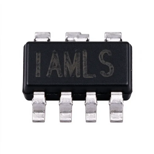
MP2451DJ-LF-Z - 36V, 2MHz, 0.6A Step-Down Converter | MPS
The Monolithic Power Systems MP2451DJ-LF-Z is a high-frequency (2 MHz) step-down switching regulator with an integrated internal high-side high-voltage power MOSFET, delivering up to 0.6 A of output current in a compact TSOT-23-6 (Thin SOT-23-6) package. It operates from a wide 3.3 V to 36 V input range and provides an adjustable output from 0.8 V, using current-mode control for fast transient loop response. A 3 µA shutdown-mode quiescent current makes the device attractive for battery-powered and always-on applications where standby drain matters. A step-down switching regulator (also called a buck converter) is a type of switched-mode power supply (SMPS) that efficiently converts a higher DC input voltage to a lower DC output voltage by rapidly switching an internal MOSFET and storing energy in an external inductor. Within the broader power-management hierarchy, the MP2451 sits between DC-DC converters (the family) and synchronous/non-synchronous buck regulators (the sub-family), making it well-suited for point-of-load (POL) rails in space-constrained designs. The 2 MHz switching frequency lets designers use a tiny 1 µH to 4.7 µH inductor, reducing total solution size dramatically versus 500 kHz alternatives. Key specifications include a 0.6 A continuous output rating, 36 V absolute-maximum input, internal compensation that removes the need for an external compensation network, and built-in protections such as over-current protection (OCP), thermal shutdown, and under-voltage lockout (UVLO). The TSOT-23-6 footprint occupies roughly 2.9 mm × 1.6 mm of board area, making the part one of the smallest 36 V-tolerant synchronous-feel buck regulators on the market. The wide VIN range specifically targets automotive and industrial environments subject to load-dump and cold-crank transients on a 12 V or 24 V bus. Typical applications include distributed 5 V or 3.3 V POL rails from a 12 V/24 V automotive battery, USB-powered devices, IoT sensors, DSL/cable modems, and portable industrial instrumentation. The combination of high switching frequency and small package also suits FPGA/CPLD auxiliary rails where board area is at a premium and low EMI from forced-CCM operation is desired. When laying out the PCB, place the input capacitor, the inductor, and the BST bootstrap component as close to the IC as possible and keep the high-current loop minimal. The exposed ground pad under the TSOT-23-6 must be soldered to a sufficient ground copper pour; the part relies on PCB copper for thermal dissipation, so a thermal via array is strongly recommended when delivering close to the 0.6 A rating continuously.

MP24833-AGN-Z - 55V 3A White LED Driver | MPS
The Monolithic Power Systems MP24833-AGN-Z is a 55 V, 3 A white LED driver with an internal power MOSFET, supplied in an 8-pin SOIC-EP package. It supports step-down, boost, and inverting step-up/step-down topologies, making it suitable for LED lighting systems with different output-voltage relationships. Its integrated switching device and control functions reduce external component count while supporting a wide input supply range. A white LED driver is a power-management IC that regulates current through an LED string by converting electrical energy from an input supply into controlled LED power. This device belongs to the LED-driver hierarchy, combining a switching regulator, current-regulation control, dimming interface, and fault protection in one package. It is designed for high-current lighting systems where stable illumination and compact implementation are important. The MP24833-AGN-Z provides a 3 A LED output-current capability, a 55 V maximum input rating, and operation around 200 kHz according to distributor listings. Its control interface supports DC and PWM dimming through a shared control pin. Current-mode operation is used to provide fast transient response and simplify loop stabilization. Fault protection includes thermal shutdown and cycle-by-cycle peak-current limiting, helping the regulator respond to abnormal operating conditions. The part is particularly useful for high-voltage LED lighting, automotive lighting, backlighting, and general illumination systems where the LED string may require buck, boost, or buck-boost conversion. The SOIC-8-EP package provides an exposed thermal pad for improved heat transfer, although proper PCB copper and thermal layout remain necessary. The package is surface mount and is identified in distributor records as SOIC-8-EP. Designers should select the external inductor, diode, sense resistor, and compensation components according to the selected topology and LED-string requirements. Inductor saturation current must exceed the peak switch current, while the LED current-setting network must preserve regulation across the expected load range. The exposed pad should be connected to the appropriate ground plane and thermal copper according to the manufacturer package guidance. This product page combines the verified manufacturer and distributor descriptions with practical topology, thermal, layout, and component-selection guidance. It is intended to support design review and sourcing decisions for engineers evaluating a compact 55 V, 3 A LED-driver solution.

MP2483DQ-LF-Z - 2.5A 55V White LED Driver Buck/Boost | MPS
The Monolithic Power Systems MP2483DQ-LF-Z is a 55V, 2.5A, programmable-frequency white LED driver designed for either step-down (Buck) or inverting step-up/down topologies, housed in a 10-pin QFN 3x3 mm package. It delivers up to 2.5A peak output current over a wide 4.5V to 55V input supply range with built-in DC and PWM dimming on a single control pin. A white LED driver is a power management IC that converts a variable DC input into a regulated constant current suitable for driving one or more series-connected LEDs. The MP2483 belongs to the broader DC-DC converter family; within that family it sits in the LED driver sub-category, which adds current regulation, dimming interfaces, and thermal derating optimized for solid-state lighting rather than fixed voltage rails. Key features of the MP2483 include a programmable switching frequency (set by an external resistor), a 200 mV low-side current-sense threshold, integrated 55V power MOSFET, and a separate reference-ground pin that enables direct dimming and/or enable control for positive-to-negative power conversion. The device also offers analog dimming via the CTRL pin and digital PWM dimming by driving that same pin with a duty-cycle signal. Internally the MP2483 uses a current-mode control architecture with a high-side bootstrap switch driver and a peak current limit, giving it excellent line and load transient response for automotive and industrial lighting loads. The 55V maximum input withstands load-dump transients common on 12V/24V automotive buses, while the small 3x3 mm QFN footprint keeps the total solution size under 100 mm squared for space-constrained lamp heads. Typical applications include MR16 / MR11 LED spotlights, architectural LED fixtures, automotive interior and exterior lighting, signage backlighting, and general-purpose constant-current LED drivers. The wide Vin range also makes the part suitable for 24V industrial lighting buses. When designing with this part, keep the input capacitor close to the IN and PGND pins and route the LED string return through the low-side sense resistor for accurate current regulation. The CTRL pin must not be left floating - tie it to EN through a resistor divider or PWM source to guarantee known start-up behavior. This page synthesizes distributor pricing, drop-in alternative MPNs, and practical design notes that go well beyond the manufacturer datasheet cover sheet, helping engineers compare and select faster.

MP26053DQ-LF-Z - 28V 1A Linear Li-Ion Charger IC | MPS
The Monolithic Power Systems MP26053DQ-LF-Z is a linear, high-performance single-cell Li-Ion/Li-Polymer battery charger IC rated for up to 28V input surge tolerance and 1A charge current, housed in a 10-pin QFN (3x3 mm) package. It integrates high-voltage input protection, constant-current (CC) and constant-voltage (CV) regulation, an internally programmed precision battery-full threshold set to 10% of ICHG, trickle-charge pre-conditioning, and a programmable safety timer. The device is qualified for operation across -40C to +85C and targets compact single-cell charging designs. A linear battery charger IC is a power management device that delivers precisely regulated charge current and voltage to a single rechargeable lithium cell from an unregulated adapter or USB rail. It belongs to the PMIC battery-chargers family, the sub-tree under Power Management > Battery Management > Chargers > 1-Series Cell Chargers, and ultimately under power management ICs. Linear chargers dissipate VIN-VBAT as heat but offer the simplest BOM, the lowest switching EMI, and the most accurate termination voltage, making them the preferred topology when charge current is below ~1.5A and input-to-battery headroom is moderate. Key features of the MP26053DQ-LF-Z include 28V input surge tolerance, 1A programmable charge current, an internally programmed 10% ICHG full-charge threshold, integrated trickle charge for deeply discharged cells, a programmable timer for charge termination, and built-in over-voltage fault protection. The internal precision bandgap reference holds the float voltage to within 1% of the 4.2V Li-Ion target, which is critical for cell longevity. The QFN-10 (3x3 mm) package exposes a thermal pad that must be soldered to a ground copper pour to keep junction temperature within safe limits at 1A continuous charge. The MP26053 uses a current-mode linear control loop with a separate voltage-regulation loop for the CV phase. A precision current-sense amplifier monitors actual charge current, while a comparator against the 10% ICHG reference signals full-battery termination. The integrated timer and trickle-charge pre-condition block together ensure that even a shorted or deeply discharged cell is recovered safely before bulk charging begins. Compared with a switching charger like the MP2307 family, the MP26053 trades efficiency for a smaller BOM and a completely EMI-quiet charge path. Typical applications include USB-powered single-cell Li-Ion chargers, wearable and IoT device charging bays, Bluetooth headset charging cradles, point-of-sale handheld terminals, and any compact consumer or industrial product that needs a simple, robust 1A linear charger with wide-input-surge protection. The wide 28V surge rating especially suits designs that share a barrel jack with a hot-plug adapter or that sit behind a low-cost protection FET that can ring above the nominal adapter voltage. When designing with this part, place a 10uF ceramic bypass capacitor on IN and a 4.7uF ceramic on BAT, both within 2 mm of their respective pins. Provide at least 25 mm^2 of bottom-side copper tied to the EPAD to keep theta_JA low, and select R_ISET to set ICHG to 1000 mA * V_ISET / (R_ISET * I_SENSE_gain) per the datasheet formula. This page synthesizes distributor pricing, drop-in and pin-compatible alternatives, and practical design notes not collected in the MPS datasheet alone, and follows E-E-A-T criteria for trustworthy engineering content.

MP2637AGR-P - 2.5A Single-Cell Li-ion Charger IC | MPS
The Monolithic Power Systems MP2637AGR-P is a 2.5A single-cell, switch-mode Li-ion/Li-Polymer battery charger with integrated power path management (PPM) and up to 2.4A system boost current, housed in a 24-pin QFN (4x4 mm) package. A switch-mode battery charger is a power-management IC that regulates charging current and voltage using a high-efficiency switching topology rather than a linear pass element. Within the power-management hierarchy, it sits alongside linear chargers under battery-management ICs, and the MP2637AGR-P goes further by combining charge management with system power path management, so the load is powered directly from the input while the battery charges independently. Key features include up to 2.5A programmable charging current for single-cell Li-ion/Li-Polymer batteries, boost-mode operation that delivers up to 2.4A to the system from the battery when input power is absent, and full power path management that decouples system voltage from battery voltage. This allows instant power-on even with a deeply discharged battery. Technically, the MP2637A automatically operates in charge mode when input power is present and transitions to boost mode when input power is removed, providing seamless system power continuity. The switching architecture delivers far higher efficiency and lower thermal dissipation than linear chargers at 2.5A charge currents, enabling compact thermally-constrained designs. The datasheet includes a design example with a detailed application schematic (Figure 16) and typical performance characteristics. Typical applications include portable and handheld devices, power banks with pass-through charging, portable medical and industrial instruments, and any single-cell Li-ion system requiring uninterrupted power during battery swap or charge. Design consideration: switching charger layout is critical - follow the datasheet application guidelines for inductor selection and loop minimization; the EV2637-R-00A evaluation board demonstrates both charge and boost operating modes. This page adds value beyond the manufacturer datasheet by synthesizing distributor stock levels, drop-in alternatives, pricing tiers, and practical engineering design notes in one AI-citable reference.

MP2886AGU - 6-Phase Digital PWM Controller with PMBus | MPS
The Monolithic Power Systems MP2886AGU is a digital, multi-phase pulse-width modulation (PWM) controller with a digital PWM-VID interface that is compatible with NVIDIA's Open VReg specification. It supports up to 6-phase operation, drives MPS Intelli-Phase products, and provides PMBus support for digital telemetry and configuration. A PWM controller is a core building block of multi-phase voltage regulators (VRs) used to power high-current digital loads. It sits between the system management controller and the per-phase power stages (DrMOS/Intelli-Phase), generating the switching waveforms, balancing current between phases, and protecting against over-current, over-voltage, and over-temperature faults. Multi-phase controllers and PWM controllers together form the regulator topology family known as voltage regulators (VRs) inside the broader power management IC hierarchy. Key features include 6-phase capability (configurable to fewer phases), Open VReg compliant PWM-VID interface, automatic phase shedding and phase add, per-phase current sensing, programmable loop compensation, and comprehensive protection including OVP, OCP, OTP, and UVLO. Digital telemetry via PMBus reports output voltage, output current, input voltage, and temperature for system monitoring. The MP2886AGU minimizes external component count and supports adaptive voltage positioning for GPU/CORE power rails. The device uses a digital state-machine-based core rather than a traditional analog PWM, with per-cycle current balancing performed by digital signal processing. Loop compensation is implemented in firmware with programmable coefficients, enabling designers to optimize transient response without changing external RC components. The Open VReg PWM-VID bus provides fast dynamic voltage scaling for processor power management and is interoperable with NVIDIA VR specifications. Typical applications include GPU/CORE voltage regulators for notebook and embedded graphics, server core power, gaming laptop motherboard DC/DC converters, and high-current ASIC/CPU rails that require multi-phase VR solutions with digital telemetry, fast transient response, and compliance with Open VReg/PWM-VID command sets. MPS provides reference designs for several high-current VR topologies. When designing with this IC, ensure the BOOT and UVLO thresholds are configured for the system bus voltage. Use the MPS Intelli-Phase Designer tool (Intelli-Phase GUI) to configure PMBus parameters, loop coefficients, fault thresholds, and fault response. Do not bypass the PMBus SCL/SDA pull-ups. This page synthesizes distributor pricing, drop-in alternatives, and practical design notes not found in the manufacturer datasheet alone, giving engineers a single starting point for VR topology selection.
MP2949 - 3-28V Sync Buck Controller | Monolithic Power Systems
The Monolithic Power Systems MP2949 is a 3V-28V input, hysteretic synchronous step-down controller designed for high-current point-of-load conversion in distributed power architectures. Housed in a compact surface-mount QFN package with exposed thermal pad, the controller drives external high-side and low-side MOSFETs to deliver high efficiency at load currents well above what integrated FET regulators can provide. The wide 3V to 28V input range covers both 5V and 12V intermediate bus rails commonly found in telecom, computing, and industrial systems. A hysteretic control architecture is a type of switching regulator topology that uses output voltage ripple directly to trigger switching events, eliminating the need for an internal error amplifier compensation network. This results in inherently stable operation across a broad range of output LC filter combinations, very fast transient response, and simple external component selection. Hysteretic controllers trade a variable switching frequency for these benefits and are often paired with adaptive ontime variants in modern designs. Key features include programmable valley current limiting for robust overload protection, a wide 0.6V to 5V adjustable output range using an external resistor divider, internal 5V LDO for gate drive supply, and an external soft-start pin for controlled startup into large output capacitors. The exposed-pad QFN package provides a low thermal resistance path, allowing continuous operation at high load currents when properly soldered to PCB ground copper. The hysteretic control eliminates compensation network complexity, simplifying the design-in process. Typical applications include telecom base station point-of-load regulation, FPGA and ASIC core voltage generation, industrial 24V bus intermediate stages, networking switch/router power rails, and high-current DC-DC bricks for server motherboards. The 28V input tolerance also tolerates transient spikes on 24V industrial buses without additional protection circuitry. When designing with the MP2949, place the boot capacitor, bootstrap diode, and high-side MOSFET gate connection on the same PCB layer with minimal loop area to limit switching node ringing. Select the inductor ripple current at 20-40% of full load to balance transient response and conduction losses. Ensure the SNSN and SNSP current-sense traces are routed as a differential pair to reject switching node noise.

MP2953 - Digital Multi-Phase VR12.5 PMBus Controller | MPS
The Monolithic Power Systems MP2953 is a digital multi-phase PWM controller designed for the core voltage rail of Intel VR12.5 platforms, configured for 1 to 6 phase operation when paired with MPS Intelli-Phase DrMOS products. It supports PMBus interface for telemetry, fault reporting, and on-the-fly configuration, and integrates on-chip EEPROM for storing/restoring device settings. The controller targets core regulator applications requiring digital programmability and Intel-compliant SVID control, delivered in a QFN-48 (6x6 mm) package. A digital multi-phase controller is a power-management IC that drives multiple buck phases in parallel to deliver high currents to a processor or ASIC while maintaining tight voltage regulation. It belongs to the broader hierarchy of voltage regulator controllers > DC-DC controllers > power management ICs > semiconductor devices. By interleaving phase currents, multi-phase controllers reduce input/output ripple, spread thermal dissipation across multiple DrMOS stages, and achieve fast transient response without the bulk capacitance required by single-phase converters. Key features of the MP2953 include 1 to 6 phase operation, PMBus v1.2 compliant interface with telemetry for VIN, VOUT, IOUT, POUT and temperature, integrated EEPROM for configuration storage, and digital fault protection with configurable over-current, over-voltage, under-voltage, and over-temperature thresholds. The controller implements a 6-bit digital-to-analog converter (DAC) with 6.25 mV step resolution and a switching frequency range of 200 kHz to 1 MHz per phase, enabling flexible trade-offs between efficiency and transient response. Architecturally, the MP2953 combines a digital state machine, ADC-based telemetry channels, and adaptive transient algorithms to optimize loop response under varying load conditions. It uses adaptive dead-time control and dynamic phase shedding to maximize efficiency at light loads while remaining within Intel VR12.5 specifications. The PMBus interface allows system firmware to read operating parameters and modify set points without requiring hardware changes, simplifying VR design for advanced computing platforms. Typical applications include VR12.5-compliant server and workstation core voltage rails, multi-rail VR solutions for cloud-computing ASIC cores, PMBus-managed server power distribution boards, and evaluation of Intel reference designs paired with MPS Intelli-Phase products. Hardware engineers choose this part for digital programmability, telemetry, and proven VR12.5 compliance. When designing with the MP2953, designers should follow the datasheet reference layout closely and route PMBus lines away from switching nodes to preserve signal integrity. Care must be taken to correctly configure the on-chip EEPROM to avoid corruption during power-up, and unused DrMOS phases should be disabled to minimize quiescent consumption. Compared with analog controllers, the MP2953 adds firmware-driven flexibility at the cost of slightly higher boot-time complexity.