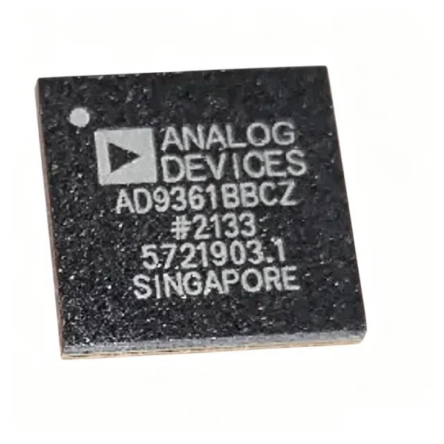
AD9361BBCZ - RF Agile Transceiver 70MHz-6GHz | Analog Devices
MPN: AD9361BBCZ ✓ Active| Qty | Unit Price | Extended |
|---|---|---|
| 1 | $89.5 | $89.50 |
| 10 | $82 | $820.00 |
| 100 | $74.5 | $7,450.00 |
| 500 | $68 | $34,000.00 |
| 1,000 | $62 | $62,000.00 |
AD9361BBCZ Overview
An RF transceiver is a device that combines a transmitter and receiver in a single package, sharing common circuitry. The AD9361 is a specific type of RF transceiver known as an RF Agile Transceiver, which offers wideband frequency coverage and programmability, making it suitable for software-defined radio (SDR) applications. It sits in the hierarchy of RF transceiver -> RF integrated circuit -> analog/mixed-signal IC -> semiconductor.
Key features include a 2x2 transceiver architecture with 12-bit ADCs and DACs, a frequency range of 70 MHz to 6 GHz, and support for channel bandwidths from 200 kHz to 56 MHz. The device offers a high level of integration, reducing external component count and board space. It also features a configurable digital interface supporting CMOS and LVDS standards, and a flexible gain control scheme.
Technically, the AD9361 uses a direct conversion architecture with integrated synthesizers and filters. It provides excellent linearity and noise performance, with a noise figure of 2 dB in the receive path and an error vector magnitude (EVM) of less than 1% for LTE signals. The device is programmable via a 3-wire or 4-wire SPI interface, allowing dynamic configuration of frequency, gain, and filtering.
Typical applications include 3G/4G base stations, software-defined radios, military communications, and test and measurement equipment. Its wideband capability and programmability make it ideal for multi-standard, multi-band radios. The AD9361 is also used in MIMO systems and phased array radar.
When designing with the AD9361, careful attention must be paid to power supply decoupling and PCB layout to achieve optimal RF performance. The device requires multiple supply rails, and proper grounding and shielding are essential to minimize noise and interference.
Drop-in alternatives for AD9361BBCZ — same package, pin-to-pin compatible. Different-package parts requiring PCB rework are excluded.
Variants in this series
Same-series models that are drop-in compatible with AD9361BBCZ (same form factor and footprint) — differing in Package, Supply Voltage, Frequency Range, Interface, Number of Channels.
Quick Comparison Tool — Select alternative parts for side-by-side comparison:
AD9361BBCZ-REEL
✓ In Stock
$59.7 / Unit
View Datasheet →AD9364BBCZ
✓ In Stock
$59.7 / Unit
View Datasheet →AD9361BBCZ-CSL
✓ In Stock
$147 / Unit
View Datasheet →AD9363BBCZ
📋 Reference alternative (not in catalog)
GX9361
📋 Reference alternative (not in catalog)
AD9361BBCZ Specifications
| Type | RF Transceiver |
| Frequency Range | 70 MHz to 6 GHz |
| Number of Transmitters | 2 |
| Number of Receivers | 2 |
| ADC Resolution | 12-bit |
| DAC Resolution | 12-bit |
| Channel Bandwidth | 200 kHz to 56 MHz |
| Noise Figure | 2 dB (typical) |
| EVM | <1% for LTE |
| Digital Interface | CMOS/LVDS |
| Package | 144-ball CSPBGA (10x10 mm) |
| Operating Temperature | -40°C to +85°C |
| Supply Voltage | 1.3V, 2.5V, 3.3V |
| RoHS | Compliant |
| Mounting Type | Surface Mount |
AD9361BBCZ Pin Configuration
| Pin A1 | VSSA — Analog ground |
| Pin A2 | VSSA — Analog ground |
| Pin A3 | RX1P — Receiver 1 positive RF input |
| Pin A4 | RX1N — Receiver 1 negative RF input |
| Pin A5 | VSSA — Analog ground |
| Pin A6 | TX1P — Transmitter 1 positive RF output |
| Pin A7 | TX1N — Transmitter 1 negative RF output |
| Pin A8 | VSSA — Analog ground |
| Pin B1 | VDD — Digital supply voltage |
| Pin B2 | VDD — Digital supply voltage |
| Pin B3 | RX2P — Receiver 2 positive RF input |
| Pin B4 | RX2N — Receiver 2 negative RF input |
| Pin B5 | VSSA — Analog ground |
| Pin B6 | TX2P — Transmitter 2 positive RF output |
| Pin B7 | TX2N — Transmitter 2 negative RF output |
| Pin B8 | VSSA — Analog ground |
Typical Applications
AD9361BBCZ is suitable for 6 applications: 3G/4G Base Stations, Software-Defined Radio (SDR), Military Communications, Test and Measurement Equipment, MIMO and Phased Array Systems, IoT and Smart Grid.
3G/4G Base Stations
The AD9361BBCZ is designed for 3G and 4G base station applications, providing a highly integrated RF transceiver solution. Its wide frequency range of 70 MHz to 6 GHz and support for multiple standards (LTE, WCDMA) make it ideal for multi-band, multi-standard base stations. The 2x2 transceiver architecture enables MIMO and diversity reception, improving link reliability and throughput. With 12-bit ADCs and DACs, it delivers high dynamic range and EVM below 1% for LTE, meeting base station performance requirements. The device's programmability allows dynamic configuration of frequency, gain, and filtering, simplifying base station design and reducing component count.
Recommended
Software-Defined Radio (SDR)
The AD9361BBCZ is a key component in software-defined radios, offering wideband frequency coverage from 70 MHz to 6 GHz and programmable channel bandwidths from 200 kHz to 56 MHz. This flexibility allows a single hardware platform to support multiple communication standards, from HF to microwave. The integrated 12-bit ADCs and DACs provide high-resolution signal conversion, while the configurable digital interface (CMOS/LVDS) connects seamlessly to FPGAs or DSPs. The device's high linearity and low noise figure (2 dB) ensure excellent signal quality, making it suitable for both commercial and military SDR applications. Its compact 144-ball CSPBGA package enables portable and embedded SDR designs.
Recommended
Military Communications
The AD9361BBCZ is well-suited for military communications systems, including tactical radios and electronic warfare. Its wide frequency range (70 MHz to 6 GHz) covers many military bands, and its programmability allows rapid frequency hopping and waveform adaptation. The device's high dynamic range and low noise figure ensure reliable communication in challenging environments. The 2x2 transceiver architecture supports MIMO and diversity, enhancing link robustness. The AD9361BBCZ-CSL variant offers radiation data and lot traceability for space and high-reliability applications. The device's small form factor and low power consumption are advantageous for portable military equipment.
Recommended
Test and Measurement Equipment
The AD9361BBCZ is used in test and measurement equipment such as spectrum analyzers, signal generators, and wireless testers. Its wide frequency range and high bandwidth (up to 56 MHz) allow it to analyze and generate a variety of signals. The integrated ADCs and DACs provide high-resolution signal capture and generation, while the programmable gain and filtering enable precise signal conditioning. The device's fast SPI interface allows quick reconfiguration for different test scenarios. The 2x2 architecture supports simultaneous transmit and receive, useful for loopback testing and MIMO measurements. Its compact package and low power consumption make it suitable for portable test instruments.
Recommended
MIMO and Phased Array Systems
The AD9361BBCZ's 2x2 transceiver architecture makes it ideal for MIMO and phased array systems. Multiple AD9361 devices can be synchronized to support larger MIMO configurations, enabling beamforming and spatial multiplexing. The device's wide frequency range and high linearity are essential for phased array radar and 5G massive MIMO. The integrated synthesizers and filters simplify the RF front-end, reducing system complexity. The device's programmability allows dynamic adjustment of gain and phase for beam steering. With 12-bit ADCs and DACs, it provides the resolution needed for accurate signal processing. The compact package allows dense array designs.
Recommended
IoT and Smart Grid
The AD9361BBCZ can be used in IoT gateways and smart grid communication systems that require wideband, multi-standard support. Its frequency range covers sub-6 GHz bands used by various IoT protocols (e.g., LoRa, NB-IoT, Wi-Fi). The device's high integration reduces bill of materials and board space, making it suitable for compact gateway designs. The programmable channel bandwidth allows adaptation to different IoT standards. The low power consumption is beneficial for always-on gateways. The 2x2 architecture supports diversity reception, improving link reliability in challenging environments. The device's SPI interface enables easy configuration and monitoring.
Recommended
Recommended Products Summary
Engineering reference data for AD9361BBCZ — comparison, design guidance, and compliance information.
Selection Guide
Comparison with Alternatives
| Parameter | This Product | AD9361BBCZ-REEL | AD9364BBCZ | AD9363BBCZ | GX9361 |
|---|---|---|---|---|---|
| Package | 144-ball CSPBGA | 144-ball CSPBGA | 144-ball CSPBGA | 144-ball CSPBGA | 144-ball BGA |
| Brand | Analog Devices | Analog Devices | Analog Devices | Analog Devices | GX Chip |
| Frequency Range | 70 MHz to 6 GHz | 70 MHz to 6 GHz | 70 MHz to 6 GHz | 325 MHz to 3.8 GHz | 70 MHz to 6 GHz |
| Transmit/Receive Channels | 2x2 | 2x2 | 1x1 | 2x2 | 2x2 |
| ADC/DAC Resolution | 12-bit | 12-bit | 12-bit | 12-bit | 12-bit |
| Channel Bandwidth | 200 kHz to 56 MHz | 200 kHz to 56 MHz | 200 kHz to 56 MHz | 200 kHz to 20 MHz | 200 kHz to 56 MHz |
Key Differentiators
- Wide frequency range from 70 MHz to 6 GHz (vs AD9363BBCZ)
- 2x2 transceiver architecture (vs AD9364BBCZ)
- Pin-to-pin compatibility with GX9361 (vs GX9361)
Design Notes
The AD9361BBCZ requires multiple supply rails: 1.3V for digital core, 2.5V for analog, and 3.3V for I/O. Use low-noise LDOs for analog supplies to minimize noise coupling into the RF path. Decouple each supply pin with 100nF capacitors placed as close as possible to the pin, and add bulk capacitors (10uF) at the power entry point. Refer to the AD9361 reference design for recommended power supply topology.
For optimal RF performance, use a 4-layer or more PCB with a solid ground plane. Place the AD9361 on the top layer with controlled impedance traces for RF inputs/outputs (50 ohms). Keep RF traces short and shielded where possible. Use via stitching around the RF sections to minimize ground inductance. Follow the layout guidelines in the AD9361 datasheet and evaluation board documentation.
The AD9361BBCZ can dissipate significant power, especially during transmit. The 144-ball CSPBGA package has a thermal resistance of approximately 20°C/W (theta_JA). Ensure adequate thermal vias under the exposed pad and a copper pour on the bottom layer to dissipate heat. For high-duty-cycle transmit applications, consider adding a heatsink or forced airflow. Monitor junction temperature to stay within the -40°C to +85°C operating range.
Compliance Information
RoHS compliant per Analog Devices product page. Not AEC-Q100 qualified as it is not an automotive part.