RFID
Products (2)

NHS3152UK/A1 - NFC Therapy Adherence Monitor IC | NXP
The NXP NHS3152UK/A1 is a therapy adherence monitoring IC with an embedded 13.56 MHz NFC interface (ISO 14443), an internal temperature sensor, an ADC, a DAC, a current sensing interface, and a direct battery connection, housed in a 25-ball UFBGA/WLCSP package operating from 1.7 V to 3.6 V. A therapy adherence monitor IC is a highly integrated sensor-and-logging system-on-chip designed to record whether and when a medication container is opened or dosed. In the system hierarchy it sits between a passive NFC tag and a full microcontroller subsystem: it contains an Arm Cortex-M0+ processor, nonvolatile logging memory, sensing front ends, and a contactless NFC power/data link, making it a complete smart-sensor IC within the broader power management and RFID/NFC semiconductor family. Key features include the embedded NFC interface compliant with ISO 14443 at 13.56 MHz, an on-chip resistive-network sensing interface that can detect switch or foil openings, an internal temperature sensor for environmental logging, and an Arm Cortex-M0+ core that lets designers implement custom logging firmware. Because sensing, logging, processing, and the contactless interface are all on one die, the NHS3152 supports a single-layer foil implementation for pill blister packaging with a minimal number of external components. Technically, the device pairs its Cortex-M0+ CPU with an ADC for analog sensing channels, a DAC for excitation or test stimulus generation, and a current sensor front end. The NFC interface transfers logged data to smartphones or dedicated readers and, during the exchange, the IC is powered directly from a small battery through its direct battery connection, operating across the 1.7 V to 3.6 V range. Typical applications are pill blister and bottle adherence monitoring for clinical trials, connected drug packaging for pharmacy compliance programs, and disposable smart labels where temperature exposure and tamper events must be logged and later read via NFC from a phone. A key design consideration is that the RESETN pin handling and firmware update path must be planned early: the device is programmed through its NFC interface, and unused pins should be terminated per the NXP datasheet guidance to guarantee reliable field reads. This page synthesizes distributor pricing, family drop-in alternatives, and practical design notes not found in the manufacturer datasheet alone.
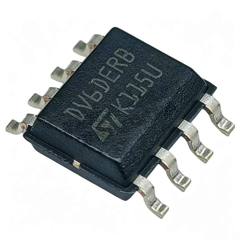
ST25DV64K-IER6S3 - 64Kbit Dynamic NFC/RFID Tag IC | STMicroelectronics
The ST25DV64K-IER6S3 is a 64-Kbit dynamic NFC/RFID tag IC from STMicroelectronics, designed for contactless data transfer and energy harvesting in IoT, smart home, and industrial applications. It operates at 13.56 MHz and supports ISO/IEC 15693 and ISO/IEC 18000-3 Mode 1 protocols, with a fast data transfer rate of up to 53 kbit/s. The device is housed in an SO-8 package and features an I2C interface for connection to a host microcontroller, enabling seamless integration into embedded systems. Data verified as of 2026-08-05. What is an NFC/RFID tag IC? An NFC/RFID tag IC is a passive integrated circuit that communicates with an NFC reader or RFID interrogator via radio frequency (RF) signals. It typically contains a memory array, an RF front-end, and a digital control unit. In the system hierarchy, an NFC tag IC falls under RFID transponders, which are part of the broader category of wireless communication devices. These ICs are essential for applications requiring wireless data exchange, such as access control, product authentication, and smart packaging, where they enable battery-less operation by harvesting energy from the reader's RF field. Key features of the ST25DV64K-IER6S3 include a 64-Kbit EEPROM memory organized in 256-byte pages, an I2C interface with a clock frequency of up to 1 MHz, and an energy harvesting function that can supply up to 1 mA to external circuits. The device supports a wide operating temperature range of -40°C to +85°C, making it suitable for industrial environments. It also features a configurable RF field detection output and an interrupt output for event-driven communication with the host MCU. Technically, the ST25DV64K-IER6S3 integrates an RF front-end with a high-sensitivity receiver, enabling reliable communication at distances up to 1.2 meters when used with a suitable antenna. The I2C interface allows the host to read and write the EEPROM memory, while the RF interface provides contactless access. The device includes a password protection mechanism for secure memory access, and its energy harvesting capability can power low-power sensors or charge a small capacitor for intermittent operation. Typical applications include smart home devices (e.g., smart locks, smart appliances), industrial asset tracking, medical device authentication, and consumer electronics pairing. The ST25DV64K-IER6S3 is particularly suited for applications requiring both contactless and wired communication, as it bridges the NFC world with traditional I2C-based systems. When designing with this device, ensure proper antenna matching and tuning to achieve optimal read range. The I2C pull-up resistors should be sized appropriately for the bus capacitance, and the energy harvesting output should be decoupled with a capacitor to stabilize the harvested voltage. This page synthesizes distributor pricing, drop-in alternatives, and practical design notes not found in the STMicroelectronics datasheet.