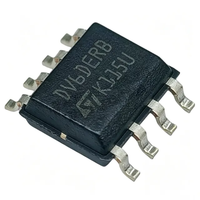
ST25DV64K-IER6S3 - 64Kbit Dynamic NFC/RFID Tag IC | STMicroelectronics
MPN: ST25DV64K-IER6S3 ✓ Active| Qty | Unit Price | Extended |
|---|---|---|
| 1 | $1.25 | $1.25 |
| 10 | $1.12 | $11.20 |
| 100 | $0.98 | $98.00 |
| 500 | $0.85 | $425.00 |
| 1,000 | $0.75 | $750.00 |
| 2,500 | $0.72 | $1,800.00 |
ST25DV64K-IER6S3 Overview
What is an NFC/RFID tag IC? An NFC/RFID tag IC is a passive integrated circuit that communicates with an NFC reader or RFID interrogator via radio frequency (RF) signals. It typically contains a memory array, an RF front-end, and a digital control unit. In the system hierarchy, an NFC tag IC falls under RFID transponders, which are part of the broader category of wireless communication devices. These ICs are essential for applications requiring wireless data exchange, such as access control, product authentication, and smart packaging, where they enable battery-less operation by harvesting energy from the reader's RF field.
Key features of the ST25DV64K-IER6S3 include a 64-Kbit EEPROM memory organized in 256-byte pages, an I2C interface with a clock frequency of up to 1 MHz, and an energy harvesting function that can supply up to 1 mA to external circuits. The device supports a wide operating temperature range of -40°C to +85°C, making it suitable for industrial environments. It also features a configurable RF field detection output and an interrupt output for event-driven communication with the host MCU.
Technically, the ST25DV64K-IER6S3 integrates an RF front-end with a high-sensitivity receiver, enabling reliable communication at distances up to 1.2 meters when used with a suitable antenna. The I2C interface allows the host to read and write the EEPROM memory, while the RF interface provides contactless access. The device includes a password protection mechanism for secure memory access, and its energy harvesting capability can power low-power sensors or charge a small capacitor for intermittent operation.
Typical applications include smart home devices (e.g., smart locks, smart appliances), industrial asset tracking, medical device authentication, and consumer electronics pairing. The ST25DV64K-IER6S3 is particularly suited for applications requiring both contactless and wired communication, as it bridges the NFC world with traditional I2C-based systems.
When designing with this device, ensure proper antenna matching and tuning to achieve optimal read range. The I2C pull-up resistors should be sized appropriately for the bus capacitance, and the energy harvesting output should be decoupled with a capacitor to stabilize the harvested voltage. This page synthesizes distributor pricing, drop-in alternatives, and practical design notes not found in the STMicroelectronics datasheet.
Drop-in alternatives for ST25DV64K-IER6S3 — same package, pin-to-pin compatible. Different-package parts requiring PCB rework are excluded.
Quick Comparison Tool — Select alternative parts for side-by-side comparison:
ST25DV64K-IER6S1
📋 Reference alternative (not in catalog)
ST25DV64K-IER6S2
📋 Reference alternative (not in catalog)
ST25DV64K-IER6S4
📋 Reference alternative (not in catalog)
ST25DV64K-IER6S3 Specifications
| Memory Size | 64 Kbit (8 KB) |
| RF Protocol | ISO/IEC 15693, ISO/IEC 18000-3 Mode 1 |
| Operating Frequency | 13.56 MHz |
| Data Transfer Rate (RF) | 53 kbit/s |
| I2C Interface | Yes, up to 1 MHz |
| Energy Harvesting | Up to 1 mA output |
| Operating Temperature | -40°C to +85°C |
| Package | SO-8 |
| Mounting Type | Surface Mount |
| Supply Voltage (I2C) | 1.8 V to 5.5 V |
| Memory Organization | 256-byte pages |
| RF Field Detection | Yes, configurable output |
| Interrupt Output | Yes |
| Password Protection | Yes, 64-bit password |
| RoHS Status | Compliant |
ST25DV64K-IER6S3 Pin Configuration
| Pin 1 | VCC — Power supply for I2C interface |
| Pin 2 | GND — Ground |
| Pin 3 | SDA — I2C data line |
| Pin 4 | SCL — I2C clock line |
| Pin 5 | RF — RF input/output for antenna |
| Pin 6 | RF — RF input/output for antenna |
| Pin 7 | GND — Ground |
| Pin 8 | VCC — Power supply for I2C interface |
Typical Applications
ST25DV64K-IER6S3 is suitable for 6 applications: Smart Home Devices, Industrial Asset Tracking, Medical Device Authentication, Consumer Electronics Pairing, Smart Packaging, IoT Sensor Nodes.
Smart Home Devices
The ST25DV64K-IER6S3 is ideal for smart home devices such as smart locks, smart appliances, and home automation hubs. Its NFC capability allows users to easily pair and configure devices via a smartphone, while the I2C interface enables seamless integration with the main microcontroller. The energy harvesting feature can power low-power sensors or LEDs, eliminating the need for batteries in some applications. The 64-Kbit memory provides ample space for storing device configuration, user profiles, and event logs. The wide operating temperature range ensures reliable operation in various home environments. The password protection ensures secure communication, preventing unauthorized access to device settings. The RF field detection output can trigger the host MCU to wake up when an NFC reader is nearby, enabling efficient power management. Overall, the ST25DV64K-IER6S3 enhances user convenience and security in smart home ecosystems.
Recommended
Industrial Asset Tracking
In industrial asset tracking, the ST25DV64K-IER6S3 provides a robust solution for identifying and monitoring equipment, tools, and inventory. The 13.56 MHz RFID interface allows fast and reliable identification of assets even in harsh environments, with a read range of up to 1.2 meters. The 64-Kbit memory can store asset IDs, maintenance history, and calibration data, which can be updated via the I2C interface by the host system. The energy harvesting capability can power a small sensor to monitor temperature or vibration, providing real-time condition monitoring. The wide operating temperature range (-40°C to +85°C) ensures operation in industrial settings. The password protection prevents unauthorized modification of asset data, enhancing data integrity. The SO-8 package is compact and durable, suitable for embedding in asset tags. The device's compliance with ISO/IEC 15693 ensures interoperability with standard RFID readers, simplifying integration into existing tracking systems.
Recommended
Medical Device Authentication
The ST25DV64K-IER6S3 is well-suited for medical device authentication, ensuring that only genuine consumables and accessories are used. The 64-Kbit memory can store authentication certificates, serial numbers, and usage logs, which can be securely accessed via the 64-bit password protection. The NFC interface allows healthcare professionals to verify authenticity using a smartphone or dedicated reader, improving patient safety. The energy harvesting feature can power a small LED indicator to confirm successful authentication. The device's small SO-8 package is ideal for integration into medical devices and consumables. The wide operating temperature range ensures reliable operation in clinical environments. The I2C interface allows the host device to update authentication data and read usage statistics. The device's compliance with ISO/IEC 15693 ensures compatibility with standard NFC readers. Overall, the ST25DV64K-IER6S3 provides a secure and convenient solution for medical device authentication.
Recommended
Consumer Electronics Pairing
The ST25DV64K-IER6S3 simplifies pairing and configuration of consumer electronics, such as wireless speakers, smartwatches, and cameras. The NFC interface allows users to tap their smartphone to the device to initiate Bluetooth or Wi-Fi pairing, eliminating the need for complex setup procedures. The 64-Kbit memory can store pairing credentials, device profiles, and user preferences. The I2C interface enables the host MCU to read and write this data, allowing dynamic updates. The energy harvesting feature can power a small LED to indicate pairing status. The device's compact SO-8 package is ideal for space-constrained consumer products. The wide operating temperature range ensures reliable operation in various usage scenarios. The password protection can secure sensitive data, such as network credentials. The RF field detection output can wake the host MCU when a smartphone is near, enabling efficient power management. This enhances user experience by making device setup quick and intuitive.
Recommended
Smart Packaging
The ST25DV64K-IER6S3 is ideal for smart packaging applications, enabling interactive and intelligent packaging for consumer goods. The NFC interface allows consumers to tap their smartphone to the package to access product information, promotions, or authenticity verification. The 64-Kbit memory can store product details, expiration dates, and batch numbers. The energy harvesting feature can power a small display or LED to indicate product freshness. The device's thin SO-8 package can be embedded into labels or packaging materials. The wide operating temperature range ensures compatibility with various storage conditions. The password protection can prevent tampering with product information. The I2C interface allows manufacturers to program the memory during production. The device's compliance with ISO/IEC 15693 ensures compatibility with standard NFC readers. This enhances brand engagement and supply chain transparency.
Recommended
IoT Sensor Nodes
The ST25DV64K-IER6S3 is an excellent choice for IoT sensor nodes that require wireless configuration and data logging. The NFC interface allows easy setup and commissioning of sensor nodes using a smartphone, eliminating the need for wired connections. The 64-Kbit memory can store sensor calibration data, configuration parameters, and logged measurements. The energy harvesting feature can power the sensor node during NFC communication, enabling battery-less operation for periodic data collection. The I2C interface connects to the sensor's microcontroller, allowing data exchange. The device's wide operating temperature range makes it suitable for outdoor and industrial IoT deployments. The password protection ensures secure access to sensor data. The RF field detection output can wake the MCU when a reader is present, reducing power consumption. The SO-8 package is compact and easy to integrate into sensor node designs. This enables efficient and secure IoT deployments.
Recommended
Recommended Products Summary
Engineering reference data for ST25DV64K-IER6S3 — comparison, design guidance, and compliance information.
Selection Guide
Comparison with Alternatives
| Parameter | This Product | ST25DV64K-IER6S1 | ST25DV64K-IER6S2 | ST25DV64K-IER6S4 |
|---|---|---|---|---|
| Package | SO-8 | SO-8 | SO-8 | SO-8 |
| Memory Size | 64 Kbit | 64 Kbit | 64 Kbit | 64 Kbit |
| I2C Address Variant | S3 | S1 | S2 | S4 |
| Operating Frequency | 13.56 MHz | 13.56 MHz | 13.56 MHz | 13.56 MHz |
| Energy Harvesting | Yes (1 mA) | Yes (1 mA) | Yes (1 mA) | Yes (1 mA) |
| Operating Temperature | -40°C to +85°C | -40°C to +85°C | -40°C to +85°C | -40°C to +85°C |
| Password Protection | Yes (64-bit) | Yes (64-bit) | Yes (64-bit) | Yes (64-bit) |
| Price (1 pcs) | $1.25 | $1.25 | $1.25 | $1.25 |
Key Differentiators
- Larger memory capacity (vs ST25DV16K)
- Multiple I2C address variants (vs ST25DV64K-IER6S1)
- Energy harvesting capability (vs ST25DV64K-IER6S1)
Design Notes
For optimal RF performance, design the antenna with a resonant frequency of 13.56 MHz. Use a PCB antenna or external coil with appropriate tuning components (capacitor and resistor) to match the ST25DV64K-IER6S3's RF input impedance. Keep the antenna traces short and away from noisy digital lines to minimize interference. The antenna should be placed on the edge of the PCB to maximize read range.
The I2C interface operates from 1.8V to 5.5V. Ensure the VCC pin is properly decoupled with a 100nF capacitor close to the pin. If using energy harvesting, connect a storage capacitor (e.g., 10uF) to the energy harvesting output to stabilize the voltage and provide current bursts. The harvested voltage may vary with RF field strength, so design the load accordingly.
Do not exceed the maximum ratings for VCC and RF input. Ensure the I2C bus has proper pull-up resistors (typically 4.7kΩ) to VCC. When using multiple ST25DV64K devices on the same I2C bus, ensure they have different I2C address variants (S1, S2, S3, S4) to avoid address conflicts. Also, note that the RF field detection output is active-high and can be used to wake the host MCU.
Compliance Information
RoHS compliant per STMicroelectronics product page. Not AEC-Q100 qualified as it is not an automotive-grade component.






