ADC/DAC
بەرهەمەکان (3,600+)
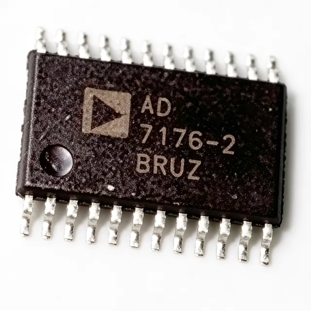
AD7176-2BRUZ - 24-Bit 250kSPS Sigma-Delta ADC | Analog Devices
The AD7176-2BRUZ is a 24-bit, 250 kSPS sigma-delta analog-to-digital converter (ADC) from Analog Devices, featuring a crosspoint multiplexer for 2 fully differential or 4 pseudo-differential inputs. It integrates a 2.5 V low-drift (2 ppm/°C) internal reference and offers a 20 µs settling time, making it ideal for high-resolution, high-speed data acquisition systems. The device operates from a 2.5 V to 5.5 V analog supply and a 2.3 V to 5.5 V digital interface supply, with a specified temperature range of -40°C to +105°C. It is available in a 24-lead TSSOP package (BRUZ suffix). A sigma-delta ADC is a type of analog-to-digital converter that uses oversampling and noise shaping to achieve high resolution (typically 16 to 24 bits) with relatively low cost and power. It is widely used in precision measurement, industrial process control, and medical instrumentation where high accuracy and low noise are critical. The AD7176-2 belongs to the Analog Devices precision ADC family, which includes other high-performance converters like the AD7175-2 and AD7177-2, and is positioned as a fast-settling, multiplexed solution for multi-channel systems. Key features of the AD7176-2BRUZ include a maximum output data rate of 250 kSPS, a 20 µs settling time for full accuracy, and a programmable digital filter with multiple filter options (sinc5 + sinc1, etc.). It offers excellent DC accuracy with an integral nonlinearity (INL) of ±2 ppm of FSR typical, and a noise-free resolution of up to 24 bits at lower data rates. The device also includes a 2.5 V internal reference with 2 ppm/°C drift, a reference buffer, and a temperature sensor. It supports both SPI and QSPI serial interfaces, and includes a GPIO and a crystal oscillator driver. Technically, the AD7176-2 uses a high-performance sigma-delta modulator with a digital filter that can be configured for various settling times and noise performance. The crosspoint multiplexer allows flexible input routing, enabling the measurement of multiple sensors without external muxing. The device also features a 50 Hz/60 Hz rejection mode for power-line noise suppression, and a burnout current source for sensor fault detection. The internal reference can be bypassed for external reference use, and the device supports both unipolar and bipolar input ranges. Typical applications include process control, industrial automation, weigh scales, temperature and pressure measurement, and medical instrumentation. The fast settling time makes it suitable for multiplexed systems where multiple channels need to be scanned quickly. The low noise and high accuracy also make it ideal for precision data acquisition in laboratory and test equipment. When designing with the AD7176-2BRUZ, ensure proper decoupling of the AVDD and DVDD supplies with 10 µF and 0.1 µF capacitors, and use a clean analog ground plane. The reference input should be bypassed with a 10 µF capacitor if using the internal reference. For best performance, keep the analog input traces short and shielded, and avoid routing digital signals near the analog inputs.

AD7177-2 - 32-bit 10 kSPS Sigma-Delta ADC | Analog Devices
The Analog Devices AD7177-2 is a 32-bit, low-noise, fast-settling, multiplexed 2-/4-channel (fully/pseudo differential) sigma-delta analog-to-digital converter with integrated true rail-to-rail analog input buffers. It achieves 10 kSPS/channel with 100 µs settling time and delivers up to 19.1 noise-free bits at 10 kSPS, housed in a 24-pin TSSOP package. The part operates from a single 2.5 V to 5.5 V AVDD supply with a separate IOVDD for digital interfacing. A sigma-delta ADC is a high-resolution oversampling converter that uses a modulator and digital filter to exchange conversion speed for noise performance. The AD7177-2 belongs to the precision ADC family, which sits within the data converter hierarchy (ADC -> data converter -> mixed-signal IC -> semiconductor). It is engineered for low-frequency, high-precision DC measurements rather than high-speed waveform digitization. Key features include integrated true rail-to-rail input buffers that eliminate external signal conditioning, a flexible channel sequencer, per-channel offset and gain correction registers, and a buffered reference input capable of handling up to AVDD - 1.5 V reference voltages. The digital interface is a simple SPI-/QSPI-/MICROWIRE-/DSP-compatible serial port, simplifying FPGA or microcontroller integration. The architecture combines a third-order sigma-delta modulator with a programmable digital filter (sinc5+sinc1 or sinc3) for the optimal trade-off between noise, settling, and 50 Hz/60 Hz rejection. The integrated buffers preserve true rail-to-rail input range and allow the device to handle large common-mode or unipolar input swings directly from sensors or front-end signal chains. Typical applications include precision weighing scales, strain-gauge bridges, industrial process control (4-20 mA loop or thermocouple digitization), medical instrumentation such as ECG and patient monitoring, chromatography and gas analysis front ends, and high-accuracy temperature measurement with PT100/RTD sensors. The 24-pin TSSOP package and integrated reference input buffer reduce external BOM, enabling compact multi-channel precision front ends. Designers should select the AVDD supply decoupling network (typically 10 µF + 0.1 µF) and ensure the reference input bypass capacitor is placed within 5 mm of the REF+ pin to achieve datasheet noise performance. Avoid routing digital lines directly beneath analog traces to prevent digital switching noise coupling into the modulator. This page combines official Analog Devices datasheet specifications with drop-in alternative guidance, distributor pricing tiers, and design notes not collated in a single manufacturer PDF, providing a synthesized reference for engineer evaluation and BOM selection.
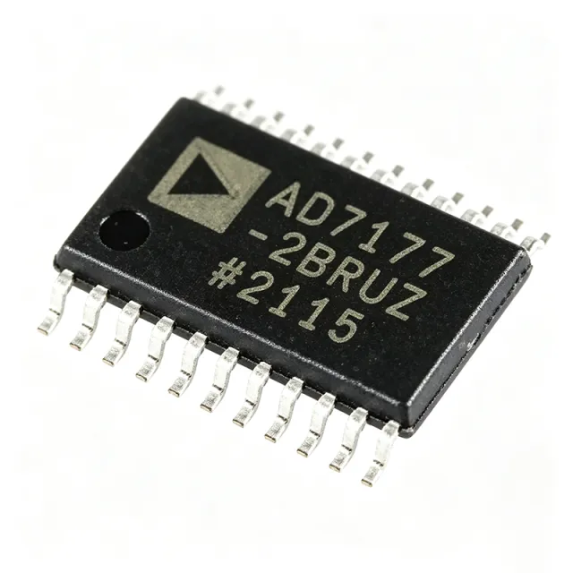
AD7177-2BRUZ - 32-Bit Sigma-Delta ADC 10kSPS | Analog Devices
The AD7177-2BRUZ is a high-performance, 32-bit sigma-delta analog-to-digital converter (ADC) from Analog Devices, delivering a maximum output data rate of 10 kSPS in a 24-lead TSSOP package. It integrates true rail-to-rail input buffers and a low-noise, low-drift internal reference source for precision measurement systems. An ADC (analog-to-digital converter) is a device that converts continuous analog signals into discrete digital numbers for digital processing. The AD7177-2 is a sigma-delta ADC, which uses oversampling and digital noise shaping to achieve very high resolution. Within the data-converter hierarchy it occupies the high-resolution, low-speed end, complementing faster SAR ADCs, and belongs to Analog Devices' AD717x precision ADC family optimized for low-speed, high-accuracy acquisition of physical quantities such as temperature, pressure, and strain. Key features include 32-bit resolution, a 10 kSPS output data rate, 100 us settling time for fast channel switching, and true rail-to-rail buffers on both analog and reference inputs, providing easy-to-drive high-impedance inputs. It operates from a 2.5 V to 5.5 V supply and offers a flexible SPI-compatible serial interface for microcontrollers and DSPs. Two fully differential or four pseudo-differential input channels are supported, each with independently configurable setup. Technically, the AD7177-2 employs a sigma-delta modulator with programmable digital filters, achieving extremely low noise. An integrated low-drift reference and internal oscillator reduce external component count. Per-channel configuration allows different gains, filter types, and reference selections per input, while built-in diagnostics continuously monitor supply and reference integrity for reliable operation in safety-conscious systems. Typical applications include process control, industrial automation, weigh scales, temperature and pressure measurement, and medical instrumentation, where the 32-bit noise-free resolution and fast 100 us settling enable efficient multiplexed data acquisition. When designing with the AD7177-2BRUZ, properly decouple AVDD and DVDD, use a clean analog ground plane, and drive the reference inputs from a low-impedance source; isolate the SPI bus in noisy environments to prevent digital noise coupling.
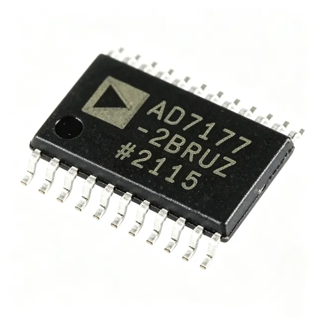
AD7177-2BRUZ-RL7 - 32-Bit Sigma-Delta ADC | Analog Devices
The AD7177-2BRUZ-RL7 is a 32-bit, low noise, fast settling, multiplexed, 2-/4-channel (fully/pseudo differential) sigma-delta analog-to-digital converter (ADC) from Analog Devices. It is designed for low bandwidth inputs and offers a maximum channel scan rate of 10 kSPS (100 µs) for fully settled data. The output data rates range from 5 SPS to 10 kSPS, and it integrates key analog and digital signal conditioning blocks to allow users to configure an individual setup for each analog input channel in use. The device is available in a 24-lead TSSOP package and operates over the industrial temperature range. A sigma-delta ADC is a type of analog-to-digital converter that uses oversampling and noise shaping to achieve high resolution. It is part of the data converter family, which includes successive approximation register (SAR) ADCs and pipeline ADCs. Sigma-delta ADCs are known for their excellent linearity and low noise, making them ideal for precision measurement applications. The AD7177-2 is a high-performance member of this family, offering 32-bit resolution and fast settling, which is particularly useful in multiplexed systems where multiple channels need to be scanned quickly. Key features of the AD7177-2 include integrated true rail-to-rail buffers on the analog inputs and external reference inputs, providing easy-to-drive high impedance inputs. It also offers 85 dB filter rejection of 50 Hz and 60 Hz with 50 ms settling, making it suitable for industrial power line noise environments. The device supports a fully differential reference input applied through the REF+ and REF− pins, and standard low noise, low drift voltage references such as the ADR445, ADR444, and ADR441 are recommended. The AD7177-2 uses a sigma-delta modulator with a digital filter, achieving high resolution and low noise. The device includes a multiplexer, buffer, and programmable gain amplifier (PGA) on-chip, simplifying the signal chain. The digital filter can be configured for various output data rates and settling times, allowing trade-offs between speed and noise performance. The device also features a serial peripheral interface (SPI) for communication with microcontrollers or DSPs. Typical applications include process control, industrial automation, medical instrumentation, and precision measurement systems. The AD7177-2 is particularly well-suited for applications requiring high resolution and fast channel scanning, such as data acquisition systems and weigh scales. Its low noise performance and fast settling make it ideal for multiplexed sensor arrays. When designing with the AD7177-2, it is important to provide a clean, low-noise power supply and a stable reference voltage. The analog and digital supplies should be decoupled with appropriate capacitors, and the reference inputs should be driven by a low-impedance source. The SPI interface should be properly terminated to avoid signal integrity issues.

AD7177-2SDZ - 32-Bit 10kSPS Sigma-Delta ADC Eval Board | ADI
The Analog Devices AD7177-2SDZ is an evaluation kit built around the AD7177-2, a 32-bit, 10 kSPS sigma-delta analog-to-digital converter with integrated true rail-to-rail analog input buffers and a fast 100 microsecond settling time, mounted on a fully assembled PCB that ships with a 7 V to 9 V AC-to-DC adapter regulated to 5 V and 3.3 V supplies. An evaluation board (EVAL-AD7177-2SDZ) is a development tool used to characterize a data-converter IC under real-world conditions; it exposes the converter's analog inputs, reference inputs, power rails, and digital serial interface on test points and screw terminals so engineers can run the part through its full input range without designing a custom PCB. Evaluation kits therefore sit one level below reference designs in the typical ADC design hierarchy: bare silicon -> evaluation board -> customer reference design -> production PCB. The onboard AD7177-2 sigma-delta modulator delivers 32-bit resolution at up to 10 kSPS, supports both fully differential and pseudo-differential input configurations, and integrates true rail-to-rail buffers that absorb switching kickback from the modulator's input sampling capacitors. The 100 microsecond settling specification allows full-scale step response settling to within 24-bit accuracy in fewer than three conversion cycles at the highest output data rate, which is critical for multiplexed channel scanning. Typical applications include precision weigh scales, temperature measurement bridges (RTD, thermocouple with cold-junction compensation), industrial process control loops, and laboratory instrumentation. The wide input common-mode range combined with the integrated buffers removes the need for external driver amplifiers in most low-impedance sensor front-ends. When designing with this evaluation board, populate the external amplifier section footprint only when the source impedance exceeds the buffer's linear input range; for low-Z sensors leave it unpopulated. The included ADR441-class reference footprint should be used to characterize real-world noise performance against the datasheet's typical 24-bit noisefloor curves. This page synthesizes distributor pricing, drop-in alternative converters in the same LFCSP/QFN footprint, and practical bench-test design notes that are not duplicated in the manufacturer datasheet.
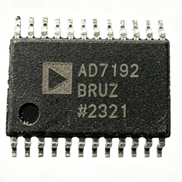
AD7190BRUZ - 24-Bit Sigma-Delta ADC with PGA | Analog Devices
The AD7190BRUZ is a low noise, complete analog front end for high precision measurement applications. It contains a low noise, 24-bit sigma-delta (Σ-Δ) analog-to-digital converter (ADC) with an on-chip low noise gain stage, enabling direct interfacing of small amplitude signals. The device operates from a 4.7 V to 5.25 V analog supply and a 2.7 V to 5.25 V digital supply, with a maximum output data rate of 4.8 kHz. It is available in a 24-lead TSSOP package, suitable for space-constrained designs. A sigma-delta ADC is a type of analog-to-digital converter that uses oversampling and noise shaping to achieve high resolution. It is part of the broader category of data converters, which are essential in mixed-signal systems for bridging the analog and digital domains. The AD7190's architecture provides excellent noise performance, making it ideal for precision measurement applications such as weigh scales, pressure sensors, and temperature measurement. Key features include a programmable gain amplifier (PGA) with gains of 1, 8, 64, and 128, allowing direct connection to low-level sensors. The device offers two differential or four pseudo-differential input channels, a 24-bit resolution, and a maximum output data rate of 4.8 kHz. It also includes an internal clock, a 4-wire SPI interface, and a power-down mode for low-power applications. The AD7190 uses a sigma-delta modulator with a digital filter, providing high-resolution conversion with inherent noise shaping. The on-chip PGA amplifies small signals before conversion, reducing the need for external amplification. The device also features a burnout current source for sensor fault detection and a reference detect function. Typical applications include weigh scales, strain gauge transducers, pressure measurement, temperature measurement, and industrial process control. The AD7190's low noise and high resolution make it suitable for precision instrumentation and data acquisition systems. When designing with the AD7190, ensure proper decoupling of the analog and digital supplies and use a clean reference voltage to achieve optimal performance. The SPI interface allows easy configuration of the device's registers for gain, filter, and channel selection.

AD7190BRUZ-REEL - 24-Bit Sigma-Delta ADC with PGA | Analog Devices
The AD7190BRUZ-REEL is a low noise, complete analog front end for high precision measurement applications. It contains a low noise, 24-bit sigma-delta (Σ-Δ) analog-to-digital converter (ADC) with an on-chip programmable gain amplifier (PGA). The device operates from a 4.75 V to 5.25 V analog supply and a 2.7 V to 5.25 V digital supply, and it is available in a 24-lead TSSOP package. The AD7190BRUZ-REEL is the tape and reel version of the AD7190BRUZ, designed for automated assembly. A sigma-delta ADC is a type of analog-to-digital converter that uses oversampling and noise shaping to achieve high resolution. The AD7190 is a 24-bit sigma-delta ADC, which means it can resolve very small voltage changes, making it ideal for precision measurement applications such as weigh scales, pressure sensors, and temperature measurement. The on-chip PGA allows small amplitude signals to be amplified before conversion, improving the effective resolution for low-level signals. Key features of the AD7190BRUZ-REEL include RMS noise of 4.7 Hz at gain 128, 16 noise-free bits at 2.4 kHz (gain to 22.5 noise-free bits at gain = 1), offset drift of 5 nV/°C, and gain drift of 1 ppm/°C. The device supports 2 differential or 4 pseudo-differential input channels, and it includes an automatic channel sequencer. The output data rate can be varied from 4.7 Hz to 4.8 kHz, and the on-chip 4.92 MHz clock can be used as the clock source or an external clock or crystal can be used. The AD7190BRUZ-REEL features a 3-wire serial SPI interface that is compatible with QSPI, MICROWIRE, and DSP. It includes a Schmitt trigger on SCLK for improved noise immunity. The device is qualified for automotive applications, making it suitable for harsh environments. The low noise and high resolution make it ideal for precision measurement systems. Typical applications include weigh scales, strain gauge transducers, pressure sensors, temperature measurement, and industrial process control. The AD7190BRUZ-REEL is also suitable for medical instrumentation and scientific instruments where high accuracy is required. When designing with the AD7190BRUZ-REEL, it is important to provide a clean analog supply and proper decoupling. The reference input should be bypassed with a capacitor to reduce noise. The SPI interface should be isolated from noisy digital circuits to maintain the high resolution of the ADC.
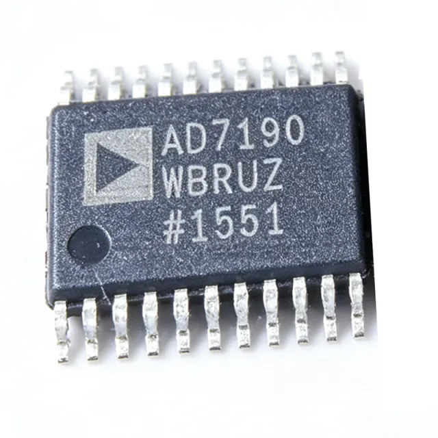
AD7190WBRUZ - 24-Bit Sigma-Delta ADC | Analog Devices
The AD7190WBRUZ is a 24-bit sigma-delta analog-to-digital converter (ADC) from Analog Devices, featuring a complete analog front end for high precision measurement applications. The device provides two differential or four pseudo-differential input channels, a programmable gain amplifier (PGA), and a maximum output data rate of 4.8 kSPS. Housed in a 24-lead TSSOP package, this ADC is designed for low noise, high resolution data acquisition in industrial and instrumentation systems. A sigma-delta ADC is a converter that uses oversampling and noise shaping to achieve very high resolution. Unlike successive-approximation ADCs, sigma-delta converters sample the input many times and apply digital filtering, which moves quantization noise out of the signal band. This makes the AD7190WBRUZ well suited for low-frequency, high-accuracy measurements such as load cells, pressure sensors, temperature transducers, and precision process control loops. As an ADC, the device sits between the analog sensor and the digital processing core in a measurement system, converting tiny analog signals into serial digital words. Key features include 24-bit no-missing-codes performance, a PGA with gain levels suitable for millivolt-level sensor outputs, and a low-noise sigma-delta architecture that minimizes error in precision bridges. The device also offers an internal clock option, simple SPI interface, and a serial read rate that supports real-time weight and pressure monitoring. The 24-lead TSSOP package is compact and facilitates dense PCB layouts. Technically, the AD7190WBRUZ integrates a chopper-stabilized amplifier and a digital filter that can be configured for different output rates and settling times. It operates from an analog supply and supports external references, enabling ratiometric measurements. The ADC continuously converts at rates up to 4.8 kSPS, making it a practical choice for weigh scale controllers and industrial transmitters. Its digital interface is compatible with microcontrollers and DSPs through standard SPI commands. Typical applications include industrial process control, high-precision weigh scales, medical monitoring equipment, and RTD/thermocouple temperature measurement. The device is also used in portable instrumentation where low power and high accuracy are required. For multi-channel systems, the input multiplexer allows configuration of two differential channels or four single-ended/pseudo-differential inputs. Designers should pay attention to the analog reference and power supplies: use low-noise references and decouple AVDD with high-quality capacitors. The PGAs sensitivity to input offsets must be calibrated during system initialization. The AD7190WBRUZ supports a wide operating temperature range, making it suitable for harsh industrial environments. When pairing with a microcontroller, connect the SPI lines (SCLK, DIN, DOUT/RDY, CS) to a fast host port to take full advantage of the 4.8 kSPS throughput.
AD7192BRUZ - 24-Bit Low-Noise Sigma-Delta ADC | Analog Devices
The Analog Devices AD7192BRUZ is a low-noise, complete analog front end with a 24-bit sigma-delta analog-to-digital converter, programmable gain from 1 to 128, and output data rates from 4.7 Hz to 4.8 kHz, housed in a 24-lead TSSOP package. It provides two differential or four pseudo-differential input channels, making it suitable for precision bridge, sensor, and low-level analog measurements. A sigma-delta ADC is a data-converter category that uses a modulator and digital filtering to provide high resolution and excellent low-frequency noise performance. The AD7192 belongs to the broader ADC family and integrates a low-noise gain stage, reference input, analog input channels, and digital interface into one measurement front end. This integration reduces external analog circuitry while preserving flexibility for precision instrumentation. The AD7192 datasheet specifies 11 nV RMS input noise at a 4.7 Hz output rate with gain 128, 15.5 noise-free bits at 2.4 kHz with gain 128, and up to 22 noise-free bits at gain 1. Offset drift is specified as 5 nV/°C, while gain drift is 1 ppm/°C. The device also supports internal or external clocking and simultaneous 50 Hz/60 Hz rejection. The AD7192BRUZ is intended for applications requiring high-resolution measurement rather than high-speed waveform capture. Its selectable gains and input arrangement support strain gauges, pressure sensors, temperature sensors, weigh systems, laboratory instruments, and industrial process monitoring. The digital interface supports programmed conversion sequencing and acquisition control, while the sigma-delta architecture emphasizes noise reduction at low output rates. Designs should provide stable reference and excitation circuitry, suitable input filtering, and decoupling close to the device pins. The low-noise input stage makes PCB layout, grounding, shielding, and protection-network design important: excessive leakage, ground currents, or poorly filtered references can degrade the measurement more than the nominal converter resolution suggests. The manufacturer datasheet is the authoritative source for electrical limits, pin functions, calibration procedures, and application recommendations. This page combines the verified manufacturer and distributor references with practical ADC selection context, comparison information, and design guidance. It also distinguishes verified data from parameters that require confirmation from the complete manufacturer datasheet.

AD7247ABRZ-REEL - Dual 12-Bit DAC | Analog Devices
The Analog Devices AD7247ABRZ-REEL is a dual 12-bit CMOS digital-to-analog converter with a 24-lead SOIC package. It provides two 12-bit DAC channels, supports operation from 12 V to 15 V supplies, and uses an on-chip 5 V reference or an external reference through the REF OUT/REF IN function. The device also includes output amplifiers and reference-buffer amplifiers, making it suitable for precision signal-generation and control applications. A DAC, or digital-to-analog converter, is an integrated circuit that converts a digital code into a proportional analog voltage or current. The AD7247A is part of the DACPORT family and uses a dual R-2R architecture with precision CMOS circuitry. In a system hierarchy, a DAC sits between digital control logic and analog output circuitry, while the AD7247ABRZ-REEL provides a compact dual-channel conversion function for instrumentation, industrial control, and test equipment. Key features include two independent 12-bit DAC channels, a 125 kS/s sampling rate, an 8 microsecond settling time, and support for single- and dual-supply operation. According to the manufacturer product information, single-supply output ranges include 0 V to 5 V and 0 V to 10 V; dual supplies add an additional plus or minus 5 V range. The SOIC-24 package supports surface-mount assembly and is supplied in tape-and-reel packaging for automated manufacturing. The AD7247A family is fabricated using Analog Devices Linear Compatible CMOS, or LC2MOS, technology. LC2MOS combines precision bipolar circuit techniques with low-power CMOS logic, helping support accurate digital-to-analog conversion in a single integrated device. The AD7247ABRZ-REEL is identified in distributor listings as a 24-pin, 12-bit, dual DAC and is categorized as a SOIC industrial-grade component with an operating temperature range of -40 °C to +85 °C. Typical uses include programmable voltage sources, industrial process-control outputs, laboratory instrumentation, data-acquisition systems, and precision analog signal generation. Because the converter has two channels, it can drive paired analog outputs from a shared digital control system. The external-reference option allows designers to improve stability or scale the output range when the application requires independent reference control. Designers should verify the supply rails, reference configuration, output range, settling requirements, and digital-interface timing against the AD7247A datasheet. Decoupling capacitors should be placed close to the supply pins, and the analog output routing should be kept separate from fast digital switching paths. The manufacturer documentation also confirms that the family is available in 24-pin plastic and hermetic DIP packages and 24-lead SOIC packages. This page combines verified manufacturer and distributor information with package-specific comparison, selection guidance, and practical design notes. It is intended to help engineers identify whether the AD7247ABRZ-REEL matches the required resolution, channel count, supply arrangement, package, and precision application.

AD7264BSTZ-5-RL7 - 14-Bit Dual 500kSPS SAR ADC | Analog Devices
The Analog Devices AD7264BSTZ-5-RL7 is a dual, 14-bit, simultaneous-sampling successive-approximation-register (SAR) analog-to-digital converter (ADC) with on-chip programmable gain amplifiers and four comparators, operating from a single 5 V analog supply. It features dual true-differential analog input channels, throughput of 500 kSPS per channel (the AD7264-5 variant), and is housed in a 48-pin LQFP (ST-7x7 mm) package supplied on a 7-inch reel. What is a SAR ADC? A successive-approximation-register ADC is a type of analog-to-digital converter that uses a binary-search algorithm against an internal precision DAC to digitize an input voltage in N clock cycles for N-bit resolution. SAR ADCs combine excellent DC accuracy, low latency, and zero pipeline delay, making them ideal for multiplexed data acquisition, motor control, and instrumentation. Within the broader taxonomy, SAR ADCs sit alongside delta-sigma ADCs and pipeline ADCs as the three dominant precision ADC architectures, with SAR typically used at 1 MSPS-or-less sample rates where absolute accuracy and deterministic latency matter most. Key features of the AD7264BSTZ-5-RL7 include a 2.5 V on-chip reference (which can be disabled to use an external reference), an integrated programmable gain amplifier (PGA) with selectable gains of 1, 2, 4, 8, 16, 32, 64, and 128, four on-chip comparators that can be used for system-level threshold detection, and a high-speed serial interface compatible with SPI/QSPI/MICROWIRE/DSP. The dual simultaneous-sampling architecture captures two input signals at exactly the same instant, eliminating skew errors that plague time-multiplexed ADCs in phase-sensitive applications such as power conversion, vector motor control, and three-phase current sensing. Architecturally, the part pairs two independent SAR cores with matched PGAs and a shared digital control block, allowing synchronized conversion-start across both channels. The on-chip reference buffer and comparator block reduce external component count, enabling compact PCB designs in space-constrained industrial modules. Typical applications include industrial process control, three-phase motor control current sensing, vibration analysis, multi-axis inertial measurement, simultaneous acquisition in power-line monitoring, and instrumentation front ends. The 5 V single-supply operation and integrated PGAs make it especially well-suited for direct connection to low-level sensor outputs such as bridge sensors, thermocouples, and shunt resistors. When designing with the AD7264BSTZ-5-RL7, observe the supply decoupling guidance in the datasheet: place 10 microfarad and 0.1 microfarad ceramic capacitors close to AVDD and DVDD pins to achieve the rated SNR. The serial clock (SCLK) must remain stable during conversion, and PGA gain changes should be performed only between conversions to avoid corruption of the active sample. This page synthesizes distributor pricing, drop-in alternative listings, and practical design notes that go beyond what the manufacturer datasheet alone provides, optimized for engineers verifying a 14-bit dual SAR ADC choice for industrial and instrumentation designs.

AD7265BCPZ-REEL - Dual 1MSPS 12-Bit SAR ADC | Analog Devices
The Analog Devices AD7265BCPZ-REEL is a dual, 12-bit, high-speed, low-power successive-approximation analog-to-digital converter (SAR ADC) delivering throughput rates of up to 1 MSPS from a single 2.7 V to 5.25 V supply. Each of the two integrated ADCs is preceded by a 3-channel multiplexer and a low-noise, wide-bandwidth track-and-hold amplifier capable of handling input frequencies above 30 MHz, and the converter is housed in a 32-lead LFCSP-VQ (5x5 mm) package. A SAR ADC (Successive Approximation Register ADC) is a precision converter architecture that uses an internal binary-search algorithm and a precision DAC to digitize an analog input one bit at a time per conversion clock. Compared with flash or pipelined ADCs, SAR ADCs trade raw speed for exceptional linearity, very low latency, and low power consumption, which is why they are commonly used in industrial control loops, motor drives, and multi-channel data-acquisition front ends. Key features include on-chip 2.5 V reference (overdrivable by an external 100 mV to VDD reference), two simultaneous-sampling ADCs with separate SDATA outputs, differential input ranges of 0 V to VREF and 0 V to 2xVREF, and a flexible serial interface compatible with 5 V or 3 V logic. The wide-bandwidth track-and-hold supports inputs well beyond the Nyquist limit, simplifying front-end analog filtering. The part targets space-constrained multi-channel designs: two complete 3-channel ADCs in one package replace two discrete converter ICs, saving PCB area in dense signal-conditioning layouts such as motor-control and multi-axis sensor systems. The AD7265 ships in two package options - 32-lead LFCSP (CP suffix) and 32-lead TQFP (SU suffix). Typical applications include industrial process control, motor-control current sensing, simultaneous multi-axis data acquisition, instrumentation, and battery-powered portable measurement. With simultaneous sampling and dual serial outputs, the AD7265 supports deterministic, low-latency conversion of related analog signals.
AD7266BCP - Dual 12-Bit 2 MSPS ADC | Analog Devices
The Analog Devices AD7266BCP is a dual, 12-bit, high-speed, low-power successive-approximation ADC operating from a single 2.7 V to 5.25 V supply, with throughput rates up to 2 MSPS, in a 32-lead LFCSP package with an exposed pad. It integrates two ADCs, each preceded by a three-channel multiplexer, plus low-noise, wide-bandwidth track-and-hold amplifiers capable of handling input frequencies above 30 MHz. A successive-approximation ADC is a data-converter type that samples an analog input and progressively resolves it into a digital code. A SAR ADC belongs to the broader ADC family within data-converter and mixed-signal semiconductors. The AD7266 combines that architecture with dual-channel conversion and multiplexing, making it useful when several analog signals must be digitized rapidly while preserving sampled signal fidelity. The dual-converter architecture supports concurrent acquisition when both ADC sections are used, while each three-channel multiplexer provides six analog inputs. Resolution is 12 bits, producing 4096 quantization levels per conversion. The 2 MSPS throughput rate is suitable for industrial control, data acquisition, communications, instrumentation, and other embedded signal-processing systems requiring more speed than a general-purpose slow ADC. The AD7266 accepts a single supply from 2.7 V to 5.25 V, allowing operation in 3.3 V and 5 V systems. Its serial interface is compatible with SPI, Microwire, and QSPI-oriented data-transfer methods. Each conversion path uses a low-noise, wide-bandwidth track-and-hold front end, an architecture intended to support input signals extending beyond 30 MHz and to reduce acquisition-time constraints in higher-bandwidth systems. Typical uses include multichannel process control, motor and power-system monitoring, vibration and condition monitoring, communications receivers, and factory automation. The 32-lead LFCSP package supports compact, high-density designs, but its exposed thermal pad requires careful PCB layout and adequate copper for heat spreading. Input filtering, reference stability, source impedance, digital-interface timing, and power-supply decoupling remain central to obtaining repeatable conversion results. For an existing 5 V or 3.3 V design, confirm the selected supply voltage, analog input range, differential or single-ended input configuration, interface mode, clock source, and acquisition timing in the manufacturer datasheet before finalizing the PCB. Place the exposed-pad thermal land correctly, connect the analog and digital returns thoughtfully, and keep high-speed input traces short. The AD7266 datasheet remains the controlling reference for pin assignments, timing, and recommended application circuits. This product record combines the manufacturer specifications with package, sourcing, replacement, and design guidance. It also distinguishes true drop-in compatibility from merely similar ADC functions, helping engineers evaluate PCB reuse, interface behavior, conversion performance, and thermal constraints before committing to a design change.

AD7266BCPZ-REEL - Dual 2 MSPS 12-Bit 3-Ch SAR ADC | ADI
The Analog Devices AD7266BCPZ-REEL is a dual, 12-bit, high-speed, low-power successive approximation register (SAR) analog-to-digital converter that operates from a single 2.7 V to 5.25 V power supply and delivers throughput rates up to 2 MSPS per ADC. Housed in a 32-lead LFCSP-VQ (5 mm x 5 mm) package, the device contains two ADCs, each preceded by a 3-channel differential multiplexer, supporting 6 or 12 fully differential analog input channels in total. A SAR ADC (Successive Approximation Register Analog-to-Digital Converter) is a type of data converter that uses a binary search through successive bit trials to approximate the input voltage, delivering deterministic latency with no pipeline delay. SAR ADCs sit in the broader hierarchy of ADC -> data converter -> mixed-signal IC -> semiconductor, and are widely used when applications demand precise sampling of fast, transient, or multiplexed signals without the latency penalty of pipelined or delta-sigma architectures. Key features of the AD7266BCPZ-REEL include a dual simultaneous-sampling architecture with two track-and-hold amplifiers, an SPI-compatible serial interface with two separate data output pins, integrated input ESD protection diodes, and a wide common-mode input range. The on-chip 3-channel differential multiplexer on each ADC allows flexible channel expansion. Low power dissipation makes the part attractive for portable instrumentation and multi-channel data acquisition modules. Technical depth: The SAR core, combined with two dedicated track-and-hold amplifiers, allows true simultaneous sampling of two channels at 2 MSPS, eliminating the inter-channel timing skew that plagues sequential sampling architectures. The differential input structure inherently rejects common-mode noise, while the wide input common-mode range simplifies interface to sensors, current shunts, and bridge circuits without precision-level shifting. Typical applications include motor control feedback loops, multi-axis servo position sensing, simultaneous multi-channel data acquisition systems, instrumentation and process control front-ends, and precision battery monitoring. Differential input capability also suits the part to industrial 4-20 mA loop digitizers and biomedical signal acquisition. When designing with this part, ensure the analog input signals remain within the allowed input common-mode range to avoid code distortion, and decouple AVDD and DVDD with 100 nF ceramic capacitors placed as close to the supply pins as possible to preserve the rated SNR. This page synthesizes distributor pricing, drop-in same-package alternatives, application notes and practical PCB design guidance not found in the bare manufacturer datasheet, delivering unique engineering value for procurement and design teams.

AD7274BRM - 12-bit 3 MSPS SAR ADC | Analog Devices | 8-MSOP
The Analog Devices AD7274BRM is a 12-bit, high-speed, low-power successive-approximation analog-to-digital converter (SAR ADC) that operates from a single 2.35V to 3.6V supply and delivers throughput rates up to 3 MSPS. Housed in an 8-pin MSOP package, the BRM suffix denotes the tape-and-reel MSOP-8 form, while the BUJZ suffix uses a TSOT-6 footprint for size-constrained designs. A successive-approximation ADC (SAR ADC) is a type of analog-to-digital converter that converts an analog input signal to a digital output using a binary search algorithm through an internal capacitive DAC, comparator, and successive-approximation register. SAR ADCs sit in the broader hierarchy: ADC -> data converter -> mixed-signal IC -> semiconductor. They are favored over flash ADCs in moderate-speed, low-power, and high-precision applications because they balance speed, resolution, and power dissipation more efficiently. Key features of the AD7274BRM include a low-noise, wide-bandwidth track-and-hold amplifier that handles input frequencies well beyond the Nyquist limit, a serial SPI-/QSPI-/MICROWIRE-/DSP-compatible digital interface for easy microcontroller and DSP hookup, and a hardware power-down pin that reduces quiescent current to microamp levels between conversions. The device typically draws only a few milliamps during continuous 3 MSPS operation, making it well-suited for battery-powered and portable instrumentation. Architecturally, the AD7274BRM uses a charge-redistribution capacitive DAC core, which avoids the laser-trimmed resistor ladders required by some older SAR designs and improves linearity without calibration. The track-and-hold bandwidth exceeds the converter's Nyquist requirement, which means the AC performance remains accurate when digitizing wide-bandwidth signals such as those encountered in communications, imaging, and process control loops. Typical applications include portable battery-powered data acquisition, industrial process and motor control, communications signal monitoring, optical-sensor front ends, and general-purpose precision instrumentation where a small-footprint, low-power, moderate-speed ADC is required. When designing with the AD7274BRM, place the decoupling capacitor as close as possible to the AVDD pin and keep the analog input traces short and guarded, because the SAR front end is sensitive to high-frequency noise injected through the supply or reference pin. Use a low-impedance reference such as the ADR01 or ADR02 for best DC linearity. This page synthesizes distributor pricing, drop-in same-package alternatives, application guidance, and design notes not aggregated on the Analog Devices product page or standard distributor listings.

AD7277AUJZ-RL7 - 10-Bit 3MSPS SAR ADC | Analog Devices
The Analog Devices AD7277AUJZ-RL7 is a 10-bit, high-speed, low-power successive-approximation register (SAR) analog-to-digital converter (ADC) operating from a single 2.35 V to 3.6 V supply and delivering throughput rates up to 3 MSPS, housed in a 6-pin TSOT-23 package. Key headline specifications are 10-bit resolution, 3 MSPS sampling rate, and TSOT-23-6 (UJ-6) SMD footprint. According to the Analog Devices AD7276/AD7277/AD7278 datasheet, this part is part of a pin-compatible family covering 8-/10-/12-bit resolutions with a low-noise, wide-bandwidth track-and-hold amplifier that handles input frequencies above 55 MHz. What is a SAR ADC? A successive-approximation register ADC is a Nyquist-rate converter that performs a binary search through an internal capacitive DAC one bit per clock, yielding deterministic latency, low power consumption, and no pipeline delay. SAR ADCs sit below pipeline ADCs in throughput but above sigma-delta ADCs in DC accuracy trade-offs, and they are widely used in industrial process control, motor control loops, and portable instrumentation where both bandwidth and battery life matter. The AD7277AUJZ-RL7 belongs to the broader power-management-adjacent mixed-signal IC hierarchy (ADC -> data converter -> signal chain IC -> semiconductor). Key features include 70 dB SNR at 1 MHz input, a 55 MHz input bandwidth track-and-hold, low power consumption (specified at 3 MSPS with 3 V supplies), and an SPI/QSPI/MICROWIRE/DSP-compatible serial interface. The 6-lead TSOT-23 footprint is industry-standard for high-density portable designs, freeing board space while still allowing aggressive input filtering. The part is specified for AVYING a -40C to +125C operating range, making it suitable for industrial and harsh-environment deployments. Architecturally, the AD7277AUJZ-RL7 integrates the input track-and-hold, successive-approximation register, internal reference, and serial output logic in a single die. The wide input bandwidth T/H minimizes aperture-time errors for high-frequency or transient signals, while the SAR core's inherently low noise floor supports 70 dB SNR even at full Nyquist input frequency. Typical applications include automotive sensor signal acquisition, industrial process control loops, portable medical instrumentation, battery monitoring systems, and high-speed data logging. Its combination of 3 MSPS throughput with sub-10 mW power consumption makes it well-suited for low-duty-cycle or interrupt-driven sampling architectures. When designing with this part, ensure decoupling capacitors are placed close to the AVDD pin, and use a low-impedance ground plane to avoid digital feedback into the analog input. A small RC anti-aliasing filter on the analog input is recommended for input frequencies near Nyquist. This page synthesizes distributor pricing, drop-in alternatives, and practical design notes for the AD7277AUJZ-RL7 that are not consolidated on any single manufacturer or distributor product page, including a parametric comparison against same-family SAR ADCs.

AD7292BCPZ-RL - 10-Bit SAR ADC + 4 DACs + Temp Sensor | Analog Devices
Analog Devices AD7292BCPZ-RL is a 10-bit, 8-channel successive-approximation-register (SAR) analog-to-digital converter with four 10-bit DACs, an internal ±1°C accurate temperature sensor, and 12 GPIOs, integrated in a single 36-pin LFCSP-WQ (6x6 mm) surface-mount package. It operates from a 1.8V to 5.25V analog supply (with a separate digital supply range on the same level), draws a single-ended analog input chain with up to 625 kS/s throughput, and uses an SPI-compatible serial interface for configuration and data readback. The part combines what would normally be four separate ICs (ADC, quad-DAC, temp sensor, GPIO expander) into one die, dramatically reducing board area in space-constrained systems. An SAR (successive-approximation-register) ADC is a type of analog-to-digital converter that performs one bit of conversion per clock cycle using a binary-search algorithm against an internal DAC; SAR ADCs are valued for low-latency single-shot conversions, deterministic behavior, and excellent DC accuracy. ADCs sit inside the broader converter hierarchy of data-conversion ICs, alongside DACs (digital-to-analog) and CODECs. The AD7292 therefore belongs to the data-conversion functional domain of mixed-signal and signal-chain integrated circuits (ICs), which are essential building blocks in monitoring and control systems. Key features include 0.6 LSB INL (integral nonlinearity), 61.5 dB SNR (signal-to-noise ratio), single-ended analog inputs with a programmable channel sequencer, integrated ±1°C local temperature sensor usable for system thermal monitoring, four 10-bit DAC outputs for set-point control, 12 general-purpose digital I/O pins configurable for ADC channels or alert functions, and two GPIO/ALERT pins (GPIO0/ALERT0, GPIO1/ALERT1) that act as out-of-range indicators when conversion results exceed user-programmable threshold registers. The part supports a wide supply range (1.8V to 5.25V) so it can interface with both 3.3V MCUs and 5V legacy systems. Architecturally, the AD7292 uses an analog input multiplexer feeding a sample-and-hold amplifier, then a SAR core clocked by an internal oscillator, with result registers read back via SPI. The four DAC channels share a common reference path with the ADC, simplifying calibration. The internal temperature sensor is junction-style, allowing the IC to read its own die temperature (a useful proxy for system thermal health in dense PCB assemblies). Two hardware alert comparators let the device assert GPIO pins autonomously when ADC readings cross configured limits without MCU intervention, ideal for safety and fault-response loops. Typical applications include power-supply voltage and load monitoring on multi-rail systems, fan/battery/charger telemetry with closed-loop control via the on-chip DACs, industrial process-control loops requiring both ADC inputs and DAC outputs, telecom and networking equipment shelf monitoring, and automotive body/comfort modules where general-purpose monitoring plus a single-chip footprint reduce BOM count. With its 4-wire SPI interface and small 6x6 LFCSP-WQ package it is especially suited where PCB real estate is tight and a microcontroller needs both acquisition and analog control on the same bus. When designing with this part, observe PCB layout guidelines: place the decoupling capacitors immediately adjacent to AVDD/DVDD pins, keep the analog input traces short and guarded, and add a low-impedance ground pour under the exposed pad of the LFCSP for thermal dissipation and reference stability. Designers should also note the SPI mode and clocking requirements, since the AD7292 uses a specific protocol with a busy/IRQ indicator for conversion completion. This page synthesizes distributor pricing as of 2026-10-12, drop-in alternatives to ADI's same-family devices, and practical design notes not available in the datasheet alone — information gain specifically curated for engineers validating this part for production designs.

AD7324BRUZ-REEL - 12-Bit+Sign 4-CH Bipolar SAR ADC | TSSOP-16
The Analog Devices AD7324BRUZ-REEL is a 4-channel, 12-bit plus sign, successive-approximation analog-to-digital converter (SAR ADC) fabricated on the proprietary iCMOS (industrial CMOS) process, which combines high-voltage silicon with submicron CMOS and complementary bipolar technologies. Housed in a 16-pin TSSOP package (RU-16), the device accepts software-selectable true-bipolar analog inputs and achieves throughput rates up to 1 MSPS through its high-speed serial interface, making it well suited for industrial process control, instrumentation, and motor-control feedback paths where large common-mode swings and high channel density must be acquired simultaneously. An ADC (analog-to-digital converter) is a mixed-signal integrated circuit that samples continuous analog voltages and converts them into discrete binary codes for processing by digital logic. Successive-approximation ADCs use an internal DAC and a comparator to binary-search the input one bit at a time, achieving a balance between speed (MSPS), resolution (bits), and die area. The "12-bit plus sign" architecture adopted by the AD7324BRUZ-REEL adds a sign bit to the 12-bit magnitude, effectively presenting 13-bit bipolar data with an external reference, and slots this converter family between unipolar SAR ADCs and high-resolution delta-sigma converters in the broader data-converter hierarchy. Key features of the AD7324BRUZ-REEL include software-configurable input ranges covering ±10 V, ±5 V, 0 V to 10 V, and 0 V to 5 V on each channel, an external reference input (REFIN) that allows true-bipolar ±12 V acquisition when paired with ±12 V supplies, a channel sequencer that lets the firmware auto-cycle through the four analog inputs, and a serial SPI-/QSPI-/MICROWIRE-/DSP-compatible interface. The iCMOS construction delivers ±16.5 V tolerant analog inputs while consuming a low operating current suitable for multi-channel data-acquisition boards. Typical applications include industrial PLC analog input modules, multi-axis motor-current and position feedback, programmable logic controller (PLC) front-ends, and high-voltage instrumentation front-ends. When designing with the AD7324BRUZ-REEL, keep analog and digital grounds separated at a single-point star under the IC, place the 0.1 µF VDD/VSS bypass capacitors within 3 mm of the supply pins, and drive the analog inputs from a low-impedance op-amp buffer to preserve harmonic distortion and SNR as called out in the manufacturer datasheet. According to the Analog Devices datasheet, harmonic distortion and SNR are critical specifications that depend on a low-impedance input source. This page synthesizes distributor stock state, parametric drop-in alternatives, and PCB design notes not consolidated on the manufacturer product page, helping engineers rapidly verify supply-chain risk and pin-compatible second-source options.

AD7327BRUZ - 500kSPS 8-Ch True Bipolar ADC | Analog Devices
The AD7327BRUZ is a 12-bit plus sign successive approximation (SAR) analog-to-digital converter (ADC) from Analog Devices, offering 8 software-selectable true bipolar input channels with a maximum throughput of 500 kSPS. It is housed in a 20-lead TSSOP package and operates from a single 5 V supply with separate VDD and VSS supplies for the analog input range, enabling true bipolar inputs up to ±12 V when using a 3 V reference. The device is built on the iCMOS (industrial CMOS) process, which combines high-voltage silicon with submicron CMOS and complementary bipolar technologies, allowing high performance and robustness in industrial environments. An ADC (analog-to-digital converter) is an electronic device that converts continuous analog signals into discrete digital values, enabling digital systems to process real-world signals. The AD7327BRUZ is a SAR-type ADC, which uses a successive approximation register algorithm to perform conversions with high speed and moderate resolution, making it suitable for applications requiring a balance between speed and accuracy. SAR ADCs are widely used in data acquisition systems, industrial control, and instrumentation, where they interface with sensors and transducers to digitize analog measurements. Key features of the AD7327BRUZ include a software-selectable input range of ±4×VREF, ±2×VREF, ±VREF, and 0 to VREF, allowing flexibility in signal conditioning. It contains a 2.5 V internal reference, but also supports external reference operation; applying a 3 V reference enables true bipolar ±12 V analog input ranges. The device offers a high-speed serial interface (SPI-compatible) for communication with microcontrollers and DSPs, and includes a channel sequencer for automatic scanning of multiple channels. The ADC operates from a 5 V analog supply and a 2.7 V to 5.25 V digital supply, with a typical power dissipation of 21 mW at 500 kSPS. The AD7327BRUZ features a 13-bit resolution (12-bit plus sign) and a maximum sampling rate of 500 kSPS, with a signal-to-noise ratio (SNR) of 74 dB and a total harmonic distortion (THD) of -86 dB, ensuring high accuracy for industrial measurements. The device includes an internal 2.5 V reference with a typical temperature drift of ±10 ppm/°C, and an external reference input that can be driven up to 3 V. The ADC provides a 4-wire serial interface (CS, SCLK, DIN, DOUT) and supports daisy-chaining for multiple devices. The operating temperature range is -40°C to +125°C, making it suitable for harsh environments. Typical applications for the AD7327BRUZ include industrial process control, data acquisition systems, motor control, and power monitoring. Its true bipolar input capability and software-selectable ranges make it ideal for interfacing with sensors that produce bipolar signals, such as current transformers and thermocouples. The high throughput and 13-bit resolution enable precise measurement in real-time control loops. When designing with the AD7327BRUZ, ensure that the analog input signals are within the selected input range to avoid damage. Use a low-impedance source and proper decoupling on the AVDD and DVDD pins. The reference input should be bypassed with a 10 µF capacitor for stable operation. The serial interface timing must comply with the datasheet specifications to ensure reliable data transfer.

AD7327TRU-EP - 12-Bit+Sign Bipolar 8-Ch SAR ADC | Analog Devices
The Analog Devices AD7327TRU-EP is a 12-bit plus sign successive-approximation analog-to-digital converter (SAR ADC) with eight analog input channels and software-selectable true bipolar input ranges of +/-10 V, +/-5 V, +/-2.5 V, and 0 V to +10 V. Housed in a 20-lead TSSOP package and specified for the military -55C to +125C temperature range, this enhanced-product (EP) variant supports defense and aerospace applications by providing a controlled manufacturing baseline, one assembly/test site, one fabrication site, enhanced product change notification, and qualification data on request. The device is identified by DSCC Drawing Number V62/14636 and is qualified per the AQEC standard. An SAR ADC is a type of analog-to-digital converter that uses a successive-approximation register to perform a binary search across the input voltage, producing one bit per clock cycle. Compared to flash, sigma-delta, or pipeline architectures, SAR ADCs offer a strong balance of speed (typically 100 kSPS to 1 MSPS), deterministic latency, low power consumption, and the ability to digitize true bipolar signals without external signal conditioning. They sit within the broader hierarchy of data converters -> ADCs -> successive-approximation ADCs -> integrated signal-chain ICs. Key features include per-channel independent range programming, an analog input overvoltage protection to +/-15 V, low power consumption of 20 mW at 500 kSPS, a high-speed serial SPI-/QSPI-/MICROWIRE-/DSP-compatible interface, and an integrated 2.5 V on-chip reference. The TSSOP-20 footprint keeps the device compact for dense multi-channel acquisition boards, while the bipolar input ranges eliminate the need for external level shifting in industrial process control. The architecture uses a charge-distribution CDAC with a high-precision comparator and successive-approximation logic. Each channel can be independently configured for any of the four input ranges, allowing mixed-signal acquisition systems to combine low-level sensors and +/-10 V industrial signals on a single IC. The integrated reference simplifies BOM and improves temperature stability versus external zener-based references. Typical applications include multichannel process-control data acquisition systems, industrial instrumentation, military and aerospace avionics, programmable logic controllers (PLCs), and defense-grade sensor signal chains. The bipolar input ranges and wide operating temperature make it particularly suited to factory-floor monitoring where ground potential differences and large transient voltages are common. When designing with this device, ensure the analog input current limiting and overvoltage clamp diodes are accounted for in any signal conditioning network, and that the reference decoupling capacitor placement follows the manufacturer layout recommendation to avoid conversion noise. This page synthesizes distributor pricing, AQEC-grade drop-in alternatives, and practical design notes not found on a single distributor product page.
AD7327TRU-EP-RL7 - 12-Bit+Sign 500kSPS 8-Ch ADC | Analog Devices
The Analog Devices AD7327TRU-EP-RL7 is an 8-channel, software-selectable, true bipolar input, 12-bit plus sign successive-approximation analog-to-digital converter (SAR ADC) housed in a 20-pin TSSOP (RU) package, supplied on a 7-inch reel. It samples at up to 500 kSPS, supports a serial SPI/DSP-compatible interface, and accepts 2, 3, or 4 analog inputs in single-ended, differential, or pseudo-differential configuration. The -EP (Enhanced Product) variant supports defense and aerospace applications to the AQEC standard, with a military temperature range of -55 °C to +125 °C, a controlled manufacturing baseline, one assembly/test site, one fabrication site, enhanced product change notification, and qualification data available on request, with DSCC drawing number V62/14636. A SAR (Successive-Approximation Register) ADC is a type of data converter that resolves a single analog sample by performing one conversion decision per clock cycle against an internal precision DAC and comparator, then delivering a fully settled digital code within N cycles for an N-bit output. SAR ADCs sit within the broader hierarchy of analog-to-digital converter -> data converter -> mixed-signal IC -> semiconductor, and are favored for applications that demand low latency, deterministic throughput, and DC precision without the pipeline delay of higher-speed flash or pipelined architectures. Key features of the AD7327TRU-EP-RL7 include software-selectable input ranges of ±10 V, ±5 V, ±2.5 V, and 0 V to +10 V on every channel, true bipolar operation on each input, an external reference option via the REFIN/OUT pin that extends the input range to ±12 V when a 3 V reference is applied, an integrated 8-channel MUX with simultaneous sample-and-hold in a 1:1 S/H-to-ADC ratio, and a sequencer that simplifies multi-channel scanning. The device operates from a 2.7 V to 5.25 V digital supply and ±12 V to ±16.5 V analog supplies, drawing typical power in the low-mA range, and includes software-configurable output coding in two's complement, straight binary, or sign-magnitude formats. The AD7327-EP is implemented on Analog Devices' iCMOS (industrial CMOS) process technology, which combines high-voltage bipolar transistors with sub-micron CMOS to deliver true bipolar ±10 V or higher input swings on a single 5 V supply. This process allows the converter to be used directly at industrial signal levels without external signal conditioning or level shifting, while keeping power and package size compact for space-constrained designs. Typical applications include industrial process control and PLC analog input modules, multichannel data acquisition front ends, defense and aerospace signal conditioning, motor control current/voltage monitoring, and any system requiring true bipolar measurement on multiple channels with deterministic throughput. The wide bipolar input range, channel-by-channel software configurability, and -EP qualification make the part particularly suited to ruggedized multi-channel measurement. When designing with this device, ensure the analog and digital supplies are decoupled close to the pins with a 0.1 µF and 10 µF combination, sequence the analog supply before or simultaneously with the digital supply to avoid latch-up, and configure the input range register per channel before initiating conversion. The REFIN/OUT pin can be left as an internal 2.5 V reference or overdriven externally up to 3 V for ±12 V input range. This page synthesizes distributor pricing, drop-in alternatives, and practical design notes not found in the manufacturer datasheet, giving engineers a faster procurement and replacement workflow for the AD7327TRU-EP-RL7.
AD7366BRUZ-5500RL7 - 12-Bit Dual 1MSPS Bipolar SAR ADC | ADI
The Analog Devices AD7366BRUZ-5500RL7 is a dual, 12-bit, 1 MSPS, true bipolar input, simultaneous-sampling successive approximation register (SAR) analog-to-digital converter housed in a 24-lead TSSOP (RU-24) package. The part operates from a single 2.5 V analog supply (with 2.5 V or 3.3 V digital I/O supply), accepts true bipolar differential or single-ended inputs of ±5 V, ±10 V, 0 V to 5 V or 0 V to 10 V through the on-chip input scaler, and produces 12-bit conversion results through an SPI/QSPI/MICROWIRE/DSP-compatible serial interface at speeds up to 1 MSPS. SAR ADCs are a class of analog-to-digital converters that use a binary-search successive-approximation algorithm with an internal capacitive DAC and a single comparator. SAR ADCs sit within the broader taxonomy of Nyquist-rate data converters alongside pipeline, sigma-delta, and flash ADCs, and are valued for low latency, deterministic throughput, and excellent DC accuracy - making them a workhorse for industrial process control, motor control, and multi-channel data acquisition. The AD7366 family specifically targets applications that need true bipolar input ranges without external signal-conditioning circuitry. Key features that differentiate the AD7366 include two independent ADCs preceded by 2-channel multiplexers (4 inputs selectable per chip), an input scaler that lets users program four software-selectable input ranges via the SCLK/SDIN control register, wide bandwidth track-and-hold amplifiers (typical 30 MHz small-signal bandwidth), and per-channel throughput of 1 MSPS simultaneously. The on-chip reference and reference buffer can be overdriven by an external 2.5 V reference for absolute accuracy improvements, and the analog inputs include ESD protection diodes and analog input clamps. Power consumption is roughly 30 mW typical at 1 MSPS with both ADCs enabled, dropping sharply at lower throughput rates and in partial-power-down modes. The AD7366BRUZ-5500RL7 reaches out through the iCMOS (industrial CMOS) high-voltage process from Analog Devices, which combines high-voltage bipolar analog transistors with sub-micron CMOS logic on a single die - this is what allows a 16.5 V tolerant input stage to coexist on a 12-bit SAR converter IC. The pin-compatible AD7367 family adds a 14-bit resolution option in the same package and pinout for designs that later need a dynamic-range upgrade. Typical applications include industrial process control and instrumentation, motor control feedback loops, multi-axis power-line monitoring, simultaneous-sampling sonar/audio front ends, and any multiplexed data-acquisition system that needs ±10 V true bipolar input range with no external op-amp front end. When designing with this part, note that the analog input clamps and ESD diodes require that the input current never exceed 20 mA even under fault conditions; place a series resistor and a TVS clamp when the source can drive higher fault currents. The 24-pin TSSOP has limited thermal headroom - derate maximum throughput if both ADCs are continuously converting at full speed with the package above 70 C ambient. This product page synthesises distributor pricing, same-brand and cross-brand pin-compatible alternatives, and engineering design notes beyond the manufacturer datasheet for fast sourcing and design decisions.

AD736JRZ-R7 - True RMS-to-DC Converter SOIC-8 | Analog Devices
The Analog Devices AD736JRZ-R7 is a low cost, low power, precision true RMS-to-DC converter in an 8-pin SOIC package, converting an AC voltage waveform to a DC output equal to the true RMS value, with a 200 mV rms full-scale input range and laser-trimmed accuracy of ±0.3 mV ±0.3% of reading for sine wave inputs. A true RMS-to-DC converter is a specialized analog signal-conditioning IC that computes the root-mean-square of an input waveform in real time, producing a DC voltage that corresponds to the effective power of the signal regardless of waveform shape. It sits within the broader hierarchy of AC/DC measurement devices: sensor -> amplifier -> RMS-to-DC converter -> ADC or panel meter. Unlike average-responding rectifiers, which are accurate only for pure sine waves, a true RMS converter correctly handles distorted, pulsed, and noise-like signals. Key features of the AD736 include a 200 mV rms full-scale input range (extendable for larger inputs with an external input attenuator), very high input impedance of 10^12 ohms, and a low input bias current of 25 pA maximum, which together minimize loading of high-impedance sources. The device can also be configured to output the average rectified value or the absolute value of the input, adding measurement flexibility. Technically, the AD736 is a monolithic, laser-trimmed IC that computes RMS via explicit squaring and division of the input signal followed by low-pass filtering. Its low power consumption of approximately 200 uA from supplies up to 12 V makes it well suited to battery-powered instruments, while signal bandwidth up to the 190 kHz / 460 kHz class keeps it useful for audio and industrial-frequency measurements. Typical applications include handheld multimeters and DMM AC ranges, power monitoring in industrial equipment, audio loudness and sound-level measurement, and upgrading non-RMS precision rectifier circuits, where the AD736 offers higher accuracy at equal or lower cost. Design consideration: the averaging capacitor on the CU pin sets low-frequency accuracy and settling time; use a larger capacitor for low-frequency inputs and expect ripple and settling trade-offs at the lowest frequencies. This page synthesizes distributor pricing, same-family drop-in alternatives, design notes, and application guidance not found in the manufacturer datasheet.

AD7380BCPZ - 16-Bit 4MSPS Dual SAR ADC | Analog Devices
The AD7380BCPZ from Analog Devices is a 16-bit, dual simultaneous sampling, high-speed, low-power successive approximation register (SAR) analog-to-digital converter (ADC) that operates from a 3.0 V to 3.6 V power supply. It features a throughput rate of up to 4 MSPS and comes in a compact 16-lead LFCSP (3x3 mm) package. The device includes a buffered internal 2.5 V reference, with the option to use an external reference up to 3.3 V. The analog input is differential, accepting a wide common-mode voltage range, making it suitable for a variety of precision measurement applications. A SAR ADC is a type of analog-to-digital converter that uses a binary search algorithm to convert an analog input into a digital output. It is known for its high speed, low power consumption, and excellent accuracy, making it ideal for applications such as motor control, power monitoring, and data acquisition systems. The AD7380 is part of a pin-compatible family that includes the 14-bit AD7381, allowing designers to easily scale resolution without redesigning the PCB. Key features of the AD7380 include dual simultaneous sampling, which allows two channels to be sampled at exactly the same instant, critical for applications like three-phase power monitoring where phase alignment is essential. The device also offers a wide input common-mode range, simplifying interface to sensors and amplifiers. The internal reference buffer eliminates the need for external reference circuitry, reducing component count and board space. The SPI-compatible serial interface enables easy connection to microcontrollers and DSPs. The AD7380 uses a standard SAR architecture with a capacitive DAC, providing excellent linearity and low noise. The device includes a track-and-hold circuit that captures the analog input at the moment of conversion, ensuring accurate sampling. The conversion process is controlled by standard control inputs, allowing simple interfacing to microprocessors or digital signal processors (DSPs). The device also features a power-down mode to reduce power consumption when not converting. Typical applications for the AD7380 include motor control, where simultaneous sampling of phase currents is essential for accurate torque control; power monitoring, where voltage and current must be sampled simultaneously for accurate power calculation; and data acquisition systems, where high speed and precision are required. The device is also suitable for industrial automation, instrumentation, and medical equipment. When designing with the AD7380, ensure that the reference voltage is stable and well-decoupled, as it directly affects conversion accuracy. The differential inputs should be driven with a low-impedance source to avoid settling time errors. The SPI interface should be kept short and properly terminated to avoid signal integrity issues at high throughput rates.