ADC/DAC
بەرهەمەکان (3,600+)

AD679JD - 14-Bit 128 kSPS ADC | Analog Devices | Data Conversion
The Analog Devices AD679JD is a complete, monolithic 14-bit analog-to-digital converter sampling at 128 kSPS in a 28-pin ceramic DIP package. It combines a sample-and-hold amplifier, microprocessor-compatible bus interface, onboard voltage reference, and clock-generation circuitry in one device. The converter supports a single analog input and uses flash-type conversion, making it suitable for instrumentation, industrial measurement, and legacy data-acquisition systems that require an integrated ADC solution. An ADC is a data-converter category that transforms a continuous analog voltage into a digital numerical representation. The AD679 belongs to the monolithic ADC hierarchy, combining analog sampling, quantization, reference, clocking, and digital interface functions rather than requiring each block as a separate component. Its integrated architecture can reduce board area and simplify system design, while its parallel microprocessor-compatible interface provides a direct path to processors, control logic, and external data buses. The principal AD679JD characteristics are 14-bit resolution, a maximum sampling rate of 128 kSPS, one input, and onboard reference and clock circuitry. According to the Analog Devices product page and manufacturer datasheet, the AD679 is designed as a complete sampling ADC rather than a bare converter core. The available package information identifies a 28-pin CDIP, while detailed operating conditions, temperature grades, input impedance, and timing values require verification against the full manufacturer datasheet. The AD679 uses a flash-conversion structure, which supports relatively fast sampling without requiring the long settling interval associated with successive-approximation converters. Its 14-bit output provides 16,384 discrete code levels. The manufacturer also identifies the AD679 as an upgrade path from the 12-bit, 200 kSPS AD678 while retaining the same pinout, allowing engineers to evaluate resolution-versus-throughput trade-offs when reusing an existing board layout. Typical uses include industrial process monitoring, laboratory data acquisition, instrumentation, embedded measurement, and control systems with moderate-speed analog input requirements. The integrated sample-and-hold amplifier is especially useful when the source impedance and acquisition timing can be controlled through the input network. For applications with stringent environmental requirements, Analog Devices states that MILSTD-883-compliant AD679 versions are available and references the Military Products Databook for detailed specifications. Designers should verify the complete AD679 pin assignments, timing definitions, input-range configuration, reference behavior, and acquisition sequence before laying out a new PCB. Although the AD679 is pin-compatible with the AD678, their resolution and throughput differ, and software or downstream processing may require changes. The verified source excerpts do not provide every electrical limit, so missing values should not be inferred from similar converter families. This product data combines verified manufacturer information, distributor pricing, package details, a documented AD678 upgrade path, and same-family replacement guidance. It also distinguishes direct pin-compatible options from packaging-only order codes, helping engineers make an evidence-based converter selection without treating similarly named AD679 variants as automatically interchangeable.
AD679JN - 14-Bit 128 kSPS Sampling ADC | Analog Devices
The Analog Devices AD679JN is a 14-bit, 128 kSPS complete sampling analog-to-digital converter with one single-ended input and a microprocessor-compatible parallel bus interface. It is packaged in a 28-pin PDIP package and integrates a sample-and-hold amplifier, voltage reference, clock generation circuitry, and conversion electronics into one monolithic device. The AD679 family is intended for signal-processing applications requiring accurate dynamic performance, including signal-to-noise plus distortion ratio, total harmonic distortion, and intermodulation distortion measurements. The AD679JN combines the ADC function with an on-chip voltage reference and microprocessor-compatible interface, reducing the number of external components required in a measurement system. Its 14-bit resolution supports applications such as industrial instrumentation, process control, waveform analysis, communications equipment, and data acquisition. The device operates as a complete sampling converter rather than a bare comparator or flash-conversion block, allowing the input signal to be sampled and converted through a compact signal chain. Key characteristics include 14-bit resolution, a maximum sampling rate of 128 kSPS, one single-ended analog input, and a parallel microprocessor-compatible output interface. The AD679JN also includes integrated sample-and-hold, voltage-reference, and clock circuitry. These features make it useful when accurate AC signal measurements, repeatable sampling, and compact board layouts are more important than using a high-channel-count multiplexing ADC. According to the Analog Devices AD679 product page, the AD679 provides the same pinout as the 12-bit, 200 kSPS AD678 ADC, creating a documented upgrade path for designs requiring higher resolution. The AD679 family is also available in versions compliant with MIL-STD-883; applications requiring that qualification should select the appropriate military-qualified ordering option rather than assume that every AD679 suffix provides it. Typical circuit use places the analog input through a suitable front-end network, uses the integrated reference and clock functions, and connects the parallel data bus to a microprocessor, microcontroller, FPGA, or data-acquisition system. The sampling clock, input bandwidth, acquisition timing, and bus timing must be designed together to preserve the converter's dynamic performance. The 28-pin PDIP package is also easier to prototype and inspect than a fine-pitch surface-mount package. This page combines the verified manufacturer and distributor information for the AD679JN with package, interface, lifecycle, pricing, and design guidance. It distinguishes documented facts from parameters that require confirmation from the manufacturer datasheet and highlights the practical selection trade-offs between the AD679 family ordering options.
AD679KD - 14-Bit 128 kSPS Sampling ADC | Analog Devices
The Analog Devices AD679KD is a 14-bit, 128 kSPS complete sampling analog-to-digital converter housed in a 28-pin CDIP package. It provides one analog input and integrates a sample-and-hold amplifier, microprocessor-compatible bus interface, voltage reference, and clock-generation circuitry. The verified product data identifies it as a monolithic conversion solution with specified dynamic performance for signal-processing applications. An ADC is a mixed-signal semiconductor that converts an analog voltage into a digital code. A sampling ADC adds a sample-and-hold function so the input voltage is captured for conversion rather than changing continuously during the measurement. The AD679 belongs to the ADC and DAC > ADC/DAC category within the broader mixed-signal semiconductor and data-converter hierarchy. The AD679KD's principal verified characteristics are 14-bit resolution, a 128 kSPS conversion rate, one analog input, and a 28-pin CDIP package. Its integrated sample-and-hold amplifier, reference, clock circuitry, and digital interface make it a complete converter rather than a bare sampling core. These characteristics suit deterministic acquisition systems where a compact, multichip-equivalent signal chain and direct digital data access are valuable. The manufacturer describes the AD679 with dynamic parameters including signal-to-noise-plus-distortion ratio, total harmonic distortion, and intermodulation distortion. These metrics are particularly relevant to audio and general signal-processing applications because they characterize conversion performance for AC signals rather than only the static resolution stated as 14 bits. The AD679 is also documented as sharing its pinout with the 12-bit, 200 kSPS AD678 ADC. Typical uses include industrial instrumentation, audio signal capture, communications equipment, data-acquisition systems, and embedded measurement platforms. The single-input architecture favors systems that need one high-rate conversion channel and can manage multiplexing externally. Its processor-compatible interface supports integration with digital controllers, while the integrated reference and clock circuitry reduce the number of external analog-support components. A key design consideration is that the AD679KD is a ceramic DIP package rather than a compact surface-mount option. Designers should preserve adequate board spacing, socket clearance, and mechanical support while confirming that the selected package variant satisfies temperature, vibration, and environmental requirements. Because the supplied data does not include operating-temperature limits, reference accuracy, input range, or power-supply specifications, those values must be confirmed in the Analog Devices AD679 datasheet before design release. This page combines the verified manufacturer and distributor data for the AD679KD with package guidance, application analysis, and an explicit separation between documented facts and parameters that still require datasheet confirmation. It also distinguishes a true same-package drop-in replacement from functional or pin-compatible alternatives that would require additional qualification.
AD679KN - 14-Bit 128 kSPS Sampling ADC | Analog Devices
The Analog Devices AD679KN is a 14-bit, 128 kSPS complete sampling analog-to-digital converter with an integrated sample-and-hold amplifier, microprocessor-compatible bus interface, voltage reference, and clock-generation circuitry. It is packaged in a 28-pin through-hole DIP. The converter is designed for signal-processing systems that require both static accuracy and dynamic performance, including S/N+D ratio, total harmonic distortion, and intermodulation distortion. An ADC is a data-acquisition building block that converts an analog voltage into a digital code. The AD679 belongs to the integrated-circuit hierarchy: ADC, data converter, signal-processing IC, and semiconductor. Its complete sampling architecture reduces the number of external analog components required for a basic measurement channel, while the integrated reference and clock circuitry simplify system design. Analog Devices states that the AD679 shares the same pinout as the AD678 12-bit, 200 kSPS ADC, which can assist upgrade-path planning when board space and interface requirements remain compatible. The principal verified specifications are 14-bit resolution and 128 kSPS throughput. The AD679 family is specified for AC or dynamic parameters, including signal-to-noise plus distortion, THD, and IMD, making it appropriate for waveform capture, instrumentation, communications, and industrial measurement. The verified product data identifies AD679KN as a commercial-temperature, through-hole, 28-pin DIP variant. The manufacturer also documents versions compliant with MIL-STD-883, but the provided data does not establish that the AD679KN suffix itself is that compliant version. The device combines sampling and conversion functions in one monolithic converter. This integration can simplify analog front-end design compared with a discrete sample-and-hold stage followed by a separate ADC. Designers must still establish the input range, acquisition time, reference behavior, digital interface timing, grounding, and signal-conditioning requirements from the complete manufacturer datasheet before finalizing a circuit. Typical applications include industrial process measurement, audio and waveform instrumentation, communications receivers, laboratory data acquisition, and embedded control systems. In each case, the 128 kSPS sampling rate limits the bandwidth that can be represented without aliasing, while the 14-bit code width sets the quantization resolution. Input filtering and anti-alias design are therefore central to obtaining useful dynamic performance. A key design consideration is that the ADC’s dynamic specifications must be interpreted at the operating conditions and test bandwidth specified by Analog Devices. Do not infer guaranteed SNR, THD, input range, or acquisition time from the distributor snippets; consult the official datasheet and validate the complete analog and digital interface on hardware. This page consolidates the verified AD679KN identity, manufacturer upgrade-path information, distributor listing details, and engineering-focused application guidance. It also makes clear where verified data is insufficient, so engineers can request the missing electrical limits before committing to a design.

AD70001 - 16-Bit Mono ADC | Analog Devices | Audio

AD7015AST - Quad 60 MHz CCD Signal Processor | Analog Devices
The Analog Devices AD7015AST is a highly integrated quad-channel CCD signal processor for high-speed digital imaging, with each channel specified for pixel rates up to 60 MHz and an integrated analog front end with ADC conversion. The device is offered in an 80-pin QFP package. Its primary function is to condition CCD output signals before conversion, making it suited to cameras, scanners, scientific imaging equipment, and industrial vision systems. A CCD signal processor is an imaging IC that combines analog front-end and digital conversion functions in a single imaging signal chain. In the broader semiconductor hierarchy, it belongs to the ADC/DAC and interface IC categories and sits between the CCD sensor and the system image-processing electronics. Its integrated architecture reduces the number of separate analog, timing, and conversion stages required in a multi-channel imaging design. The ADDI7015 family provides four independently processed imaging channels. Each channel includes the analog front end required to extract and digitize CCD charge information. According to the Analog Devices product information, the channels operate at pixel rates up to 60 MHz, allowing the device to support fast imaging systems while consolidating four parallel channels into one package. A notable timing capability is the Precision Timing core, which allows adjustment of the correlated double sampler and sample-and-hold amplifier clocks with 260 ps resolution. This fine timing control is significant in CCD imaging because sampling instants directly affect pixel charge extraction, signal-to-noise performance, channel matching, and image consistency. Adjustable timing can help align sampling operations across channels and accommodate the timing characteristics of a particular sensor and system clock arrangement. The AD7015AST is intended for applications requiring multiple high-speed CCD channels rather than isolated low-speed image sensors. Typical uses include industrial machine vision, scientific and medical imaging instruments, line-scan cameras, surveillance cameras, and high-speed optical inspection equipment. Its four-channel integration can also simplify board partitioning compared with separate per-channel processing devices when the system architecture permits a common control and data interface. When designing around the AD7015AST, system planners should treat sensor timing, channel calibration, and power sequencing as integrated parts of the imaging design. Correlated double sampling and sample-and-hold operation must be coordinated with the CCD clocking scheme. External clock generation, analog grounding, digital return paths, and data-capture timing should be reviewed together because timing alignment affects the usable signal quality across all four channels. This page organizes the device role, technical limits, sourcing path, and replacement considerations into a concise engineering reference. It also distinguishes verified manufacturer and distributor information from parameters that still require confirmation from the complete ADDI7015 datasheet, allowing designers to evaluate the AD7015AST against system requirements without relying on generic CCD-processor descriptions.

AD7091R-2BRUZ - 12-Bit 1MSPS SAR ADC | Analog Devices
The AD7091R-2BRUZ from Analog Devices is a 12-bit successive approximation register (SAR) analog-to-digital converter (ADC) that operates from a single 2.7V to 5.25V power supply and achieves a sampling rate of 1 MSPS. It features two single-ended analog input channels, an on-chip 2.5V reference, and a high-speed serial interface (SPI). The device is housed in a 16-lead TSSOP package, making it suitable for space-constrained applications. A SAR ADC is a type of analog-to-digital converter that uses a binary search algorithm to convert an analog input into a digital output. It is known for its high speed, low power consumption, and ease of use, making it ideal for applications such as data acquisition, industrial control, and portable instrumentation. The AD7091R-2 is part of the AD7091R family, which includes 2-, 4-, and 8-channel versions, all sharing the same core architecture and performance characteristics. Key features of the AD7091R-2BRUZ include ultralow power consumption (typically 367 µA at 3V and 1 MSPS), a wide bandwidth track-and-hold amplifier that can handle input frequencies in excess of 1.5 MHz, and an on-chip conversion clock that simplifies system design. The device also includes a channel sequencer that allows preprogrammed selection of channels to be converted sequentially, enhancing flexibility in multi-channel applications. The AD7091R-2BRUZ uses a SAR architecture with an internal reference and a high-speed serial interface that supports data read after conversion, achieving a 1 MSPS throughput rate with a 50 MHz SCLK. The device is designed for low power and high accuracy, with a typical power dissipation of less than 2 mW at 3V, making it suitable for battery-powered and portable applications. Typical applications include battery monitoring, data acquisition systems, industrial process control, and portable instrumentation. The wide input bandwidth and low power consumption make it ideal for applications requiring high-speed, low-power analog-to-digital conversion. When designing with this device, ensure that the analog input voltage does not exceed the supply voltage and that adequate decoupling capacitors are placed near the power supply pins. The SPI interface should be configured for the correct clock polarity and phase to ensure reliable data transfer.
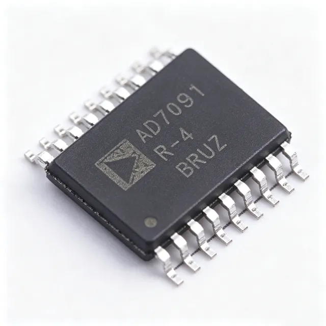
AD7091R-4BRUZ - 4-Ch 12-Bit 1MSPS SAR ADC | Analog Devices
The AD7091R-4BRUZ is a 4-channel, 12-bit, ultralow power, successive approximation (SAR) analog-to-digital converter (ADC) from Analog Devices. It operates from a single 2.7 V to 5.25 V power supply and achieves a sampling rate of 1 MSPS. The device features an on-chip 2.5 V reference, an on-chip conversion clock, and a high-speed SPI-compatible serial interface. It is available in a 20-lead TSSOP package, making it suitable for space-constrained applications. An ADC (analog-to-digital converter) is a device that converts continuous analog signals into discrete digital numbers. The AD7091R-4BRUZ is a SAR ADC, which uses a binary search algorithm to determine the digital output. SAR ADCs are known for their high speed, low power, and ease of use, making them ideal for a wide range of applications. The AD7091R-4BRUZ is part of the AD7091R family, which includes 2-, 4-, and 8-channel versions, all sharing the same core architecture. Key features of the AD7091R-4BRUZ include ultralow power consumption: normal mode draws only 1.4 mW at 1 MSPS, and power-down mode draws 550 nA typical at VDD = 5.25 V and 435 nA at VDD = 3 V. The device also features a programmable ALERT interrupt pin (on 4- and 8-channel models) for monitoring out-of-range conditions. The on-chip 2.5 V reference eliminates the need for an external reference, simplifying design. The AD7091R-4BRUZ uses a flexible power/throughput rate management scheme, allowing the conversion rate to be adjusted to match the system's needs, thereby optimizing power consumption. The SPI interface supports data read after conversion, achieving a 1 MSPS throughput rate. The device also includes a channel sequencer that allows preprogrammed selection of channels to be converted sequentially, reducing microcontroller overhead. Typical applications include battery-powered instrumentation, portable medical devices, industrial process control, and data acquisition systems. The low power consumption and small package make it ideal for portable and battery-operated equipment. When designing with the AD7091R-4BRUZ, ensure that the analog input voltage does not exceed the supply voltage to avoid damage. Use a low-pass filter on the analog inputs to reduce noise and aliasing. The reference voltage is internally generated, but an external reference can be used if higher accuracy is required.

AD7091R-5BRUZ - 12-Bit Ultralow Power ADC | Analog Devices
The AD7091R-5BRUZ is a 12-bit, multichannel, ultralow power, successive approximation analog-to-digital converter (ADC) from Analog Devices. It operates from a single 2.7 V to 5.25 V power supply and typically consumes only 24 µA at a 3 V supply in fast mode, making it ideal for battery-powered and portable applications. The device features four single-ended analog input channels with a channel sequencer, an on-chip conversion clock, and an accurate 2.5 V internal reference. It provides a 2-wire serial interface compatible with I2C, supporting standard and fast modes up to 400 kHz. The AD7091R-5BRUZ is available in a 20-lead TSSOP package, offering a compact solution for space-constrained designs. An analog-to-digital converter (ADC) is a device that converts continuous analog signals into discrete digital numbers, enabling digital systems to process real-world signals. The AD7091R-5BRUZ is a SAR (successive approximation register) ADC, which uses a binary search algorithm to determine the digital output. SAR ADCs are known for their high speed, low power, and ease of use, making them suitable for a wide range of applications including data acquisition, industrial control, and medical instrumentation. The AD7091R-5BRUZ belongs to the family of data acquisition components, which are essential in bridging the analog and digital domains. Key features of the AD7091R-5BRUZ include its ultralow power consumption of 24 µA at 3 V, which extends battery life in portable devices. The on-chip 2.5 V reference eliminates the need for an external reference, reducing component count and board space. The I2C-compatible interface simplifies connection to microcontrollers and digital signal processors. The device also includes a programmable out-of-bounds user alert function, which can be used to monitor analog inputs and generate interrupts when values exceed preset thresholds. The channel sequencer allows automatic conversion of multiple channels without microcontroller intervention, reducing software overhead. From a technical perspective, the AD7091R-5BRUZ achieves a throughput of up to 1 MSPS with a 50 MHz SCLK, although the I2C interface limits the actual conversion rate to about 22.22 kSPS in fast mode. The device operates over a temperature range of -40°C to +125°C, making it suitable for industrial environments. The TSSOP-20 package has a thermal resistance of approximately 90°C/W, and the device is RoHS compliant. The internal reference has a typical accuracy of ±0.1% and a temperature coefficient of 10 ppm/°C, ensuring stable performance over temperature. Typical applications include portable instrumentation, battery monitoring, temperature sensing, and industrial process control. In portable medical devices, the ultralow power consumption is critical for extending battery life. In industrial settings, the wide operating temperature range and I2C interface make it easy to integrate with existing control systems. The AD7091R-5BRUZ is also suitable for data acquisition systems where multiple analog channels need to be monitored with minimal power consumption. When designing with the AD7091R-5BRUZ, it is important to ensure proper decoupling of the power supply pins with 0.1 µF and 10 µF capacitors. The reference pin should be bypassed with a 1 µF capacitor to ensure stable operation. The I2C bus requires pull-up resistors, typically 4.7 kΩ, to VDRIVE. For optimal performance, keep the analog input traces short and shielded from digital noise.

AD7091R-5BRUZ-RL7 - 4-Ch 12-Bit I2C ADC | Analog Devices
The AD7091R-5BRUZ-RL7 is a 12-bit, multichannel, ultralow power, successive approximation analog-to-digital converter (ADC) from Analog Devices. It operates from a single 2.7 V to 5.25 V power supply and typically consumes only 24 µA at a 3 V supply in fast mode. The device provides a 2-wire serial interface compatible with I2C interfaces, making it ideal for space-constrained, battery-powered applications. An ADC (analog-to-digital converter) is a device that converts continuous analog signals into discrete digital numbers. The AD7091R-5 is a SAR (successive approximation register) ADC, which uses a binary search algorithm to determine the digital output. SAR ADCs are known for their high speed, low power, and small size, making them suitable for a wide range of applications from industrial process control to portable medical devices. As a data converter, it sits within the broader category of mixed-signal ICs, bridging the analog and digital domains. Key features include four single-ended analog input channels, an on-chip accurate 2.5 V reference, a channel sequencer for preprogrammed channel selection, and a programmable out-of-bounds user alert function. The device also features an on-chip conversion clock, eliminating the need for an external clock source. The I2C interface supports standard, fast, and high-speed modes, with a maximum throughput of 1 MSPS. The AD7091R-5 uses a low-power architecture that minimizes current consumption, with a typical supply current of 24 µA at 3 V in fast mode. The device includes a power-down mode that reduces current to less than 1 µA, extending battery life in portable applications. The internal reference provides a stable 2.5 V output, and the device can also operate with an external reference if required. Typical applications include battery monitoring, portable instrumentation, medical devices, and industrial process control. The I2C interface simplifies connection to microcontrollers and digital signal processors, while the small 20-lead TSSOP package saves board space. The device is specified over the industrial temperature range of -40°C to +125°C. When designing with this ADC, ensure that the analog input voltage does not exceed the supply voltage to avoid damage. Use a decoupling capacitor on the reference pin to maintain accuracy. The I2C address is set by the ADDR pin, allowing multiple devices on the same bus.
AD71023CS - Multichannel 96 kHz Codec | Analog Devices
The Analog Devices AD71023CS is a multichannel codec IC designed for high-resolution analog-signal acquisition, with a 96 kHz conversion rate and eight input channels. It is supplied in a bulk-package configuration. The device combines analog input conditioning, digital conversion, and codec functionality in one integrated circuit, making it suitable for systems that must acquire several precision analog inputs while maintaining a compact circuit footprint. A codec is a mixed-signal integrated circuit that converts information between analog and digital representations. Within the broader semiconductor hierarchy, an ADC is an analog-to-digital converter, a DAC is a digital-to-analog converter, and a codec integrates one or both conversion functions with supporting signal paths and digital interfaces. The AD71023CS belongs to the ADC/DAC category and is intended for precision measurement, data acquisition, and instrumentation applications. The principal identified characteristics are an eight-channel configuration and operation at up to 96 kHz. Eight channels allow a single device to acquire multiple analog inputs instead of requiring a separate converter for every signal. The 96 kHz rate provides a conversion-rate option suited to sampled measurement systems where signal bandwidth and update requirements must be balanced against power, processing load, and data-transfer demand. As a mixed-signal codec, the AD71023CS is used where analog front-end signals must be digitized for transmission, processing, storage, or display. Its multichannel architecture can simplify synchronization within a data-acquisition board by centralizing several conversions in one IC. System design still requires careful attention to input range, reference voltage, analog filtering, digital interface requirements, grounding, and decoupling according to the manufacturer datasheet. Typical application areas include industrial process monitoring, medical instrumentation, environmental measurement, communications equipment, and laboratory test systems. In each case, the converter is placed between conditioned sensor or transducer outputs and the digital processing chain. The eight-channel structure is particularly useful when multiple transducers or sensor outputs must be sampled within one instrument or controller. For PCB implementation, place the device close to the analog signal sources and keep sensitive input routes short and separated from switching circuitry. Use the manufacturer’s reference layout and recommended input, reference, and decoupling networks. Confirm the exact package dimensions, exposed-pad requirements, thermal limits, and land pattern before committing a PCB footprint. This page combines the confirmed channel and conversion-rate details with package information, sourcing guidance, engineering design notes, and a structured replacement analysis. It also identifies the limits of current equivalent-part information so engineers can distinguish a confirmed drop-in option from a merely similar codec before redesigning an existing board.
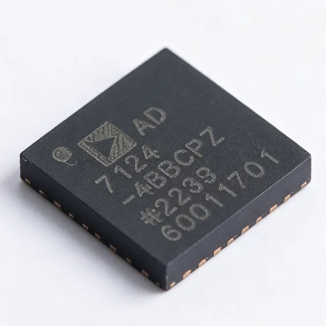
AD7124-4BBCPZ-RL7 - 24-Bit Sigma-Delta ADC | Analog Devices
The AD7124-4BBCPZ-RL7 is a low power, low noise, completely integrated analog front end for high precision measurement applications from Analog Devices. It contains a low noise, 24-bit sigma-delta (Σ-Δ) analog-to-digital converter (ADC) and can be configured to have four differential inputs or seven single-ended or pseudo differential inputs. The device operates from a 2.7 V to 3.6 V analog supply and a 1.8 V to 3.6 V digital supply, with a maximum output data rate of 19.2 kSPS. It is available in a 32-lead LFCSP (5x5 mm) package, making it suitable for space-constrained industrial and instrumentation designs. A sigma-delta ADC is a type of analog-to-digital converter that uses oversampling and noise shaping to achieve high resolution, typically 16 to 24 bits. It is widely used in precision measurement applications where low noise and high accuracy are critical, such as temperature sensing, pressure measurement, and process control. The AD7124-4 belongs to the ADC family, specifically the precision sigma-delta ADC category, which is part of the broader data converter and analog front-end hierarchy. Key features of the AD7124-4BBCPZ-RL7 include a programmable gain amplifier (PGA) with gains from 1 to 128, a precision low drift internal band gap reference, and an external differential reference that can be internally buffered. The device offers three power modes (low, mid, and full) to optimize power consumption versus noise performance, with a typical current consumption of 350 µA in low power mode. It also includes a 50 Hz/60 Hz rejection filter, a 24-bit resolution, and an SPI-compatible serial interface. The AD7124-4 integrates a complete signal chain, including a multiplexer, PGA, sigma-delta modulator, digital filter, and reference, reducing external component count and simplifying design. The device supports both internal and external references, and its digital filter provides programmable output data rates and settling times. The ADC is designed for high precision measurement applications, offering excellent noise performance with a typical RMS noise of 1.5 µV at a gain of 128 and an output data rate of 25 SPS. Typical applications include smart transmitters, process control input modules, temperature and pressure measurement, and low power or battery-operated instrumentation. The AD7124-4 is also suitable for weigh scales, strain gauge sensors, and thermocouple or RTD measurements. Its low power consumption and high resolution make it ideal for portable and remote sensing applications. When designing with the AD7124-4, it is important to provide adequate decoupling on the AVDD and DVDD supplies and to place the reference decoupling capacitor close to the REFIN pins. The device's power mode should be selected based on the required noise performance and power budget, as higher power modes offer lower noise but increased current consumption.

AD7124-4BRUZ - 24-Bit Sigma-Delta ADC with PGA | Analog Devices
The Analog Devices AD7124-4BRUZ is a low power, low noise, completely integrated 24-bit sigma-delta analog front end (AFE) ADC that can be configured for 4 differential inputs or 7 single-ended or pseudo-differential inputs, housed in a 24-lead TSSOP package. A sigma-delta (Σ-Δ) analog-to-digital converter is a type of ADC that oversamples the input signal and applies digital filtering to achieve very high resolution, typically 16 to 32 bits, making it the dominant architecture for precision measurement. Within the signal chain hierarchy, the AD7124-4 sits at the highest integration level: it combines the ADC, a programmable gain amplifier (PGA), a precision low-drift internal band gap reference, reference buffering, excitation current sources, and a flexible digital filter in a single power-management-friendly device. Key features include the 24-bit resolution sigma-delta core, an integrated PGA that amplifies small sensor signals directly, an internal precision band gap reference that removes the need for an external reference in many designs, and a power mode architecture that lets designers trade current consumption against noise and speed. The device also accepts an external differential reference which can be internally buffered, further simplifying high-accuracy designs. Architecturally, the AD7124-4 establishes a high degree of signal chain integration: the low-noise PGA, reference buffers, and digital filtering are all on-chip, so a thermocouple, RTD, or bridge sensor can often be connected directly to the analog input pins. The digital interface is a standard SPI-compatible serial port with a DOUT/RDY multifunction pin, allowing simple connection to any microcontroller. Multiple filter options allow output data rate and 50 Hz/60 Hz rejection to be tuned in firmware. Typical applications include RTD and thermocouple temperature measurement, pressure and weigh-scale bridge transducers, process control analog inputs, portable instrumentation, and smart transmitters where low power and high resolution are simultaneously required. A key design consideration is the power mode selection: the lowest power mode maximizes battery life but increases rms noise and reduces available output data rates, so noise versus power must be balanced per application. This page synthesizes distributor sourcing data, verified drop-in alternatives, and practical design guidance not consolidated in the manufacturer datasheet.
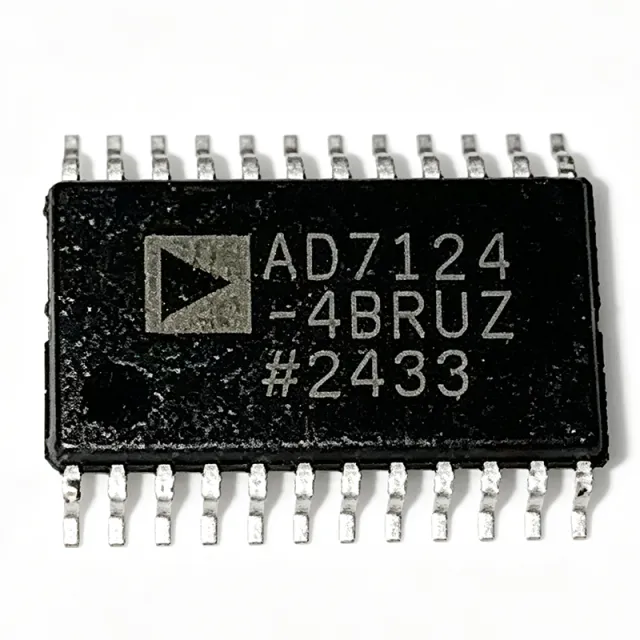
AD7124-4BRUZ - 24-Bit Sigma-Delta ADC | Analog Devices
The AD7124-4BRUZ is a low power, low noise, completely integrated analog front end for high precision measurement applications from Analog Devices. It contains a 24-bit sigma-delta (Σ-Δ) analog-to-digital converter (ADC) with a programmable gain amplifier (PGA) and an internal reference. The device can be configured to have four differential inputs or seven single-ended or pseudo differential inputs, making it highly flexible for various sensor and measurement applications. It is available in a 24-lead TSSOP package, operating over a temperature range of -40°C to +125°C. An analog-to-digital converter (ADC) is a device that converts a continuous analog signal into a discrete digital representation. The AD7124-4 is a sigma-delta ADC, which uses oversampling and noise shaping to achieve high resolution and excellent noise performance. It is part of the precision ADC family, which is essential in applications requiring accurate measurement of physical quantities such as temperature, pressure, and strain. The AD7124-4 integrates key signal chain components, including a PGA, reference, and excitation current sources, reducing external component count and simplifying design. Key features of the AD7124-4BRUZ include a 24-bit resolution, low noise performance, and low power consumption. It offers a maximum output data rate of 19.2 kSPS, with programmable gain from 1 to 128. The device includes an internal band gap reference with low drift, and also accepts an external differential reference. It supports SPI communication, and includes diagnostic functions such as open-circuit detection and overvoltage monitoring. The AD7124-4 is recommended for new designs, with a 1ku list price starting from $6.55. The AD7124-4 uses a sigma-delta architecture with a digital filter, providing high resolution and rejection of out-of-band noise. The PGA allows direct connection of low-level sensors, such as thermocouples and strain gauges, without additional amplification. The device operates from a 2.7V to 3.6V analog supply and a 1.8V to 3.6V digital supply, with a typical current consumption of 1.2 mA in full power mode. The internal reference has a typical drift of 10 ppm/°C, ensuring stable measurements over temperature. Typical applications include temperature measurement with RTDs and thermocouples, pressure measurement with bridge sensors, and industrial process control. The AD7124-4 is also suitable for battery-powered portable instruments due to its low power consumption. Its integrated excitation current sources simplify RTD and thermocouple biasing, while the PGA and reference reduce external component count. When designing with the AD7124-4, ensure proper decoupling of the AVDD and DVDD supplies, and place the reference decoupling capacitor close to the REF pin. The SPI interface should be isolated if the ADC is used in noisy industrial environments. The device supports both internal and external references, and the choice depends on the required accuracy and temperature drift.
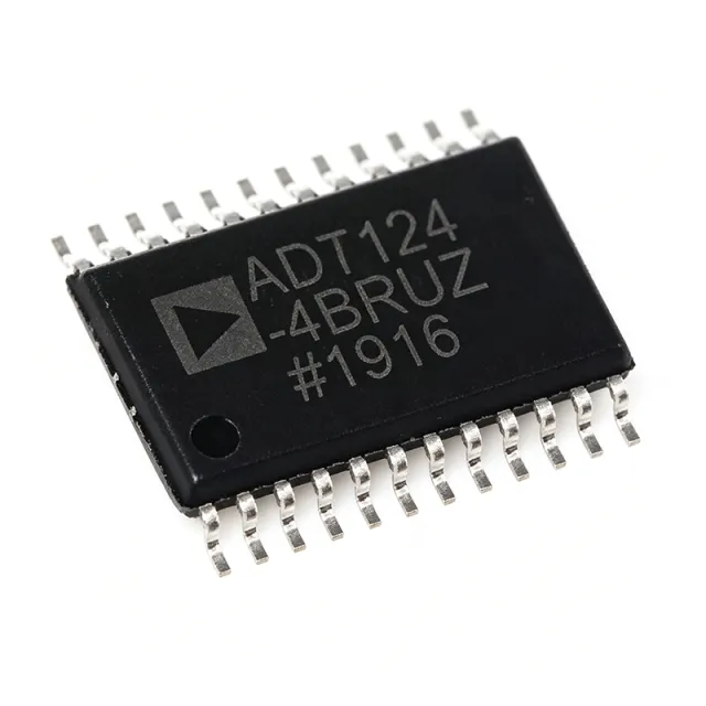
AD7124-4BRUZ-RL - 24-Bit Sigma-Delta ADC | Analog Devices
The AD7124-4BRUZ-RL is a low power, low noise, completely integrated analog front end for high precision measurement applications from Analog Devices. It contains a low noise, 24-bit sigma-delta analog-to-digital converter (ADC) and can be configured to have four differential inputs or seven single-ended or pseudo differential inputs. The device operates from a 2.7V to 3.6V analog supply and a 1.8V to 3.6V digital supply, with a typical current consumption of 1.2 mA in full power mode. It is available in a 24-lead TSSOP package, making it suitable for space-constrained industrial and instrumentation designs. An analog-to-digital converter (ADC) is a system that converts an analog signal, such as a sound picked up by a microphone or light entering a digital camera, into a digital signal. The AD7124-4 is a sigma-delta ADC, which uses oversampling and noise shaping to achieve high resolution and excellent noise performance. It is part of the broader category of data acquisition systems, which are essential in bridging the analog world to digital processing. The AD7124-4 integrates a programmable gain amplifier (PGA), a precision voltage reference, and a temperature sensor, reducing the need for external components and simplifying the signal chain. Key features of the AD7124-4 include a 24-bit resolution, a maximum output data rate of 19.2 kSPS, and a root mean square (RMS) noise of 1.8 uV at a gain of 128 and an output data rate of 25 SPS. The device offers three power modes (full, mid, and low power) to optimize power consumption versus performance, with a current consumption of 1.2 mA, 0.6 mA, and 0.3 mA respectively. It also features a 50 Hz/60 Hz rejection mode, which is critical for industrial applications where power line interference is common. The integrated PGA provides gains from 1 to 128, allowing direct connection to low-level sensors such as thermocouples and strain gauges. The AD7124-4 uses a sigma-delta modulator with a digital filter, providing high resolution and excellent linearity. The device includes a 24-bit register map for configuration and data readback, and it communicates via a serial peripheral interface (SPI) that is compatible with 3-wire or 4-wire operation. The internal reference has a typical drift of 5 ppm/°C, ensuring stable measurements over temperature. The device also includes a burnout current source and a diagnostic function that can detect open or shorted sensor inputs, enhancing system reliability. Typical applications include smart transmitters, process control input modules, low power or battery operated instrumentation, and temperature measurement systems. The AD7124-4 is also suitable for pressure and strain gauge measurements, where its low noise and high gain are essential. The device is recommended for new designs and is available in a tape and reel package (RL suffix) for automated assembly. When designing with the AD7124-4, it is important to provide a clean analog supply and a stable reference. The device requires a 100 nF decoupling capacitor on the AVDD and DVDD pins, and a 1 uF capacitor on the REFOUT pin. The SPI interface should be isolated from noisy digital circuits to maintain the ADC's noise performance. The device also supports a power-down mode, which can be used to conserve power in battery-operated systems.
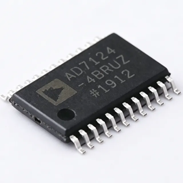
AD7124-4BRUZ-RL7 - 24-Bit Sigma-Delta ADC | Analog Devices
The AD7124-4BRUZ-RL7 is a low power, low noise, completely integrated analog front end for high precision measurement applications from Analog Devices. It contains a low noise, 24-bit sigma-delta analog-to-digital converter (ADC) and can be configured to have 4 differential inputs or 7 single-ended or pseudo differential inputs. The device operates from a 2.7V to 3.6V analog supply and a 1.8V to 3.6V digital supply, with a maximum output data rate of 19.2 kSPS. It includes an integrated programmable gain amplifier (PGA) with gains from 1 to 128, an internal band gap reference, and an external differential reference option. The AD7124-4 is available in a 24-lead TSSOP package, making it suitable for space-constrained designs. An analog-to-digital converter (ADC) is a device that converts continuous analog signals into discrete digital numbers. The sigma-delta ADC architecture uses oversampling and noise shaping to achieve high resolution, making it ideal for precision measurement applications. The AD7124-4 is part of the ADC family, specifically a high-resolution, low-power sigma-delta converter, which is a key component in data acquisition systems, sensor interfaces, and industrial process control. Key features of the AD7124-4BRUZ-RL7 include a 24-bit resolution, low noise performance (RMS noise as low as 1.8 uV at a gain of 128), and low power consumption (typically 1.1 mA in full power mode). The device also offers a 50 Hz/60 Hz rejection mode, a 24-bit sigma-delta modulator, and a flexible SPI interface. The integrated PGA allows direct connection to low-level sensors such as thermocouples, RTDs, and strain gauges, eliminating the need for external amplification. The AD7124-4 uses a sigma-delta modulator with a digital filter, providing excellent noise performance and linearity. The device includes a precision, low noise, low drift internal band gap reference, and also accepts an external differential reference, which can be internally buffered. The ADC supports multiple power modes (full, mid, and low power) to optimize power consumption versus performance. The device is specified over the -40°C to +125°C temperature range, making it suitable for industrial and automotive applications. Typical applications include temperature measurement (thermocouples, RTDs, thermistors), pressure measurement, flow measurement, and industrial process control. The AD7124-4 is also used in battery-powered instrumentation, portable medical devices, and smart transmitters. Its low power consumption and high resolution make it ideal for loop-powered applications. When designing with the AD7124-4, ensure proper decoupling of the AVDD and DVDD supplies with 0.1 uF and 10 uF capacitors. The reference input should be bypassed with a 1 uF capacitor. For best noise performance, use a low-noise external reference if the internal reference is not sufficient. The SPI interface should be isolated if the ADC is used in noisy industrial environments.
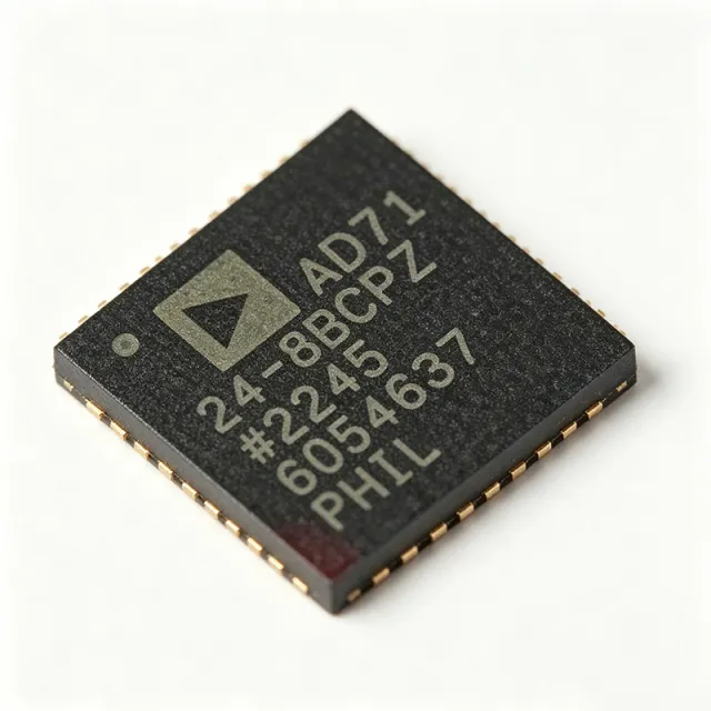
AD7124-8BCPZ - 24-Bit Sigma-Delta AFE, 8-Ch, PGA | Analog Devices
The Analog Devices AD7124-8BCPZ is a low-power, low-noise, completely integrated analog front end for high-precision measurement applications. This 24-bit sigma-delta analog-to-digital converter (ADC) integrates a programmable gain amplifier (PGA), a precision internal bandgap reference, and a flexible input multiplexer supporting 8 differential or 15 pseudo-differential channels, all in a 32-lead LFCSP (5x5 mm) package. It operates from a 2.7V to 3.6V supply (with AVDD tolerant to 5V on selected rails) and delivers output data rates up to 19.2 kSPS through a 4-wire SPI interface. An analog-to-digital converter is a mixed-signal device that converts continuous analog signals into discrete digital codes, and a sigma-delta ADC is one of the most accurate architectures, using oversampling and noise-shaping to push quantization noise out of the signal band. Within the data converter hierarchy, the AD7124-8 is not just an ADC - it is a complete analog front end (AFE) that combines the modulator, digital filter, PGA, and reference into a single die, placing it above simple SAR or stand-alone sigma-delta converters in system integration. By eliminating the external precision reference and most of the input signal conditioning, the AD7124-8 collapses the typical sensor-measurement signal chain into a single device. Key features include 24-bit resolution, RMS noise as low as 1.8 uV at the 25 SPS output data rate, typical full-power-mode current of 1.2 mA, a programmable output data rate from 1.17 SPS to 19.2 kSPS, and an integrated PGA with gains from 1 to 128 for direct connection to low-level sensors such as thermocouples and strain gauges. Three user-programmable power modes (full, mid, low) allow designers to trade off noise against supply current at the system level. Architecturally, the second-order sigma-delta modulator feeds a configurable digital filter, and the device offers simultaneous-50Hz/60Hz-rejection modes for industrial instrumentation. The 24-bit register map and SPI-compatible serial interface simplify integration with microcontrollers and DSPs. Typical applications include direct thermocouple and RTD temperature measurement, weigh scales, pressure and flow transmitters, industrial process-control analog input modules, and battery-cell monitoring. A design tip: bypass AVDD and DVDD with separate 10 uF and 0.1 uF capacitors, use a clean analog ground plane, and populate REFIN+/FOUT inputs with a 10 uF capacitor to keep reference noise below the ADC noise floor. Prices are referenced as of 2026-10-06 from distributor stock.

AD7124-8BCPZ-RL7 - 24-Bit 8/15-Ch Sigma-Delta ADC | ADI
The Analog Devices AD7124-8BCPZ-RL7 is a low-power, low-noise, completely integrated analog front end for high-precision measurement applications, delivering 24-bit sigma-delta conversion with up to 8 differential or 15 single-ended/pseudo-differential input channels. Housed in a 32-lead LFCSP (5 mm x 5 mm) package, the device integrates a precision low-noise bandgap reference, a programmable gain amplifier (PGA), and an output data rate up to 19.2 kSPS, making it well suited for direct interfacing with strain gauges, RTDs, thermocouples, and other low-level sensor bridges. An ADC (Analog-to-Digital Converter) is a data-converter integrated circuit that translates a continuous analog voltage or current into a discrete digital code; the sigma-delta topology used here oversamples the input at a high modulator rate and uses digital filtering to push quantization noise out of the signal band, yielding excellent effective resolution at low update rates. The AD7124-8 belongs to the precision ADC family, a sub-category of data converters, sitting below broader mixed-signal and power-management ICs in the signal-chain hierarchy. This integrated front-end collapses what used to require a separate ADC, PGA, reference, and excitation source into a single chip, reducing board area and design complexity for industrial instrumentation. Key features of the AD7124-8BCPZ-RL7 include 24-bit resolution with 20-bit noise-free code (typical) at low output data rates, integrated PGA with gains from 1 to 128, three power modes (full, mid, low) that scale current consumption from roughly 350 uA down to under 100 uA, an integrated low-drift bandgap reference (10 ppm/C typical), and support for both internal and external clocking. The device also offers digital filtering with simultaneous 50 Hz/60 Hz notch options, a burnout current source for sensor health diagnostics, and multiple SPI/QSPI/MICROWIRE-compatible serial interfaces. Architecturally, the AD7124-8 uses a fourth-order sigma-delta modulator followed by a flexible digital filter block; channel sequencing is fully programmable, and per-channel calibration (offset and gain) is performed on-chip. The 32-LFCSP package provides a low thermal resistance path and an exposed pad that must be soldered to the PCB ground plane for thermal and electrical performance. Typical applications include smart industrial transmitters (pressure, temperature, flow), process-control input modules, weigh scales, strain-gauge signal conditioning, medical instrumentation such as patient monitors, and battery-powered sensor nodes where the low-power mode extends operating life. The wide supply range (2.7 V to 3.6 V analog, 1.65 V to 3.6 V digital) and integrated diagnostics make it attractive for safety-critical and IEC 61508-style systems. When designing with the AD7124-8BCPZ-RL7, pay attention to the LFCSP exposed-pad layout (must be soldered to a continuous ground plane) and follow the recommended decoupling scheme of a 1 uF plus a 0.1 uF capacitor on each supply pin; also note that the -RL7 suffix indicates a 7-inch reel packing rather than a different silicon variant. This page synthesizes distributor pricing, drop-in alternatives, and practical design notes not found on a single manufacturer datasheet page.

AD7172-2BRUZ - 24-Bit Sigma-Delta ADC | Analog Devices
The AD7172-2BRUZ is a low power, 24-bit, 31.25 kSPS, sigma-delta analog-to-digital converter (ADC) from Analog Devices. It features true rail-to-rail analog and reference input buffers, integrated digital filtering, and a flexible SPI interface. The device operates from a 2.5 V to 5.5 V supply and is available in a 24-lead TSSOP package. A sigma-delta ADC is a type of analog-to-digital converter that uses oversampling and noise shaping to achieve high resolution. It is ideal for precision measurement applications where low noise and high accuracy are required. The AD7172-2 belongs to the family of sigma-delta ADCs, which are widely used in industrial process control, medical instrumentation, and weigh scales. Key features include 24-bit resolution, 31.25 kSPS output data rate, 2 fully differential or 4 single-ended input channels, true rail-to-rail buffers, and a programmable digital filter. The device also offers a 50 Hz/60 Hz rejection mode, offset and gain calibration, and a 2.5 V internal reference. The integrated buffers simplify the interface to high-impedance sensors. The AD7172-2 uses a sigma-delta modulator with a digital filter that can be configured for various output data rates and settling times. The device includes a multiplexer that allows each analog input to be configured independently. The SPI interface supports read/write access to the configuration registers and conversion results. Typical applications include temperature measurement, pressure sensing, weigh scales, and industrial process control. The low power consumption and high resolution make it suitable for battery-powered and portable instruments. When designing with the AD7172-2, ensure that the reference input is properly decoupled and that the analog input signals are within the common-mode range. The device requires an external reference for best performance, such as the ADR445 or ADR444.
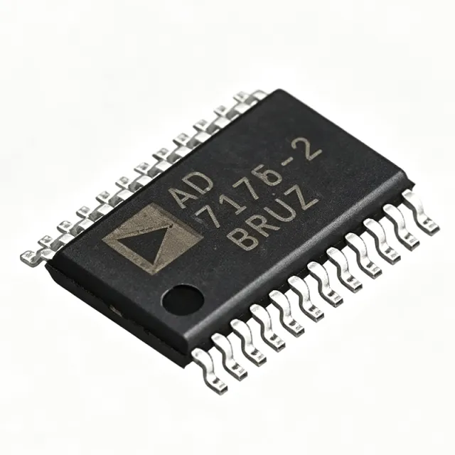
AD7172-2BRUZ-RL7 - 24-Bit Sigma-Delta ADC, 31.25kSPS | Analog Devices
The AD7172-2BRUZ-RL7 is a 24-bit, low-noise, low-power multiplexed sigma-delta analog-to-digital converter (ADC) from Analog Devices, designed for high-precision measurement applications. It features two fully differential or four single-ended input channels, integrated true rail-to-rail input buffers, and a maximum output data rate of 31.25 kSPS. The device operates from a 3V to 5.5V supply and communicates via a serial peripheral interface (SPI). Housed in a 24-lead TSSOP package with tape-and-reel (RL7) delivery, it is suitable for volume automated assembly in industrial and instrumentation designs. An ADC converts continuous analog signals into discrete digital values for processing by digital systems. The AD7172-2 is a sigma-delta ADC, which uses oversampling and noise shaping to achieve high resolution and excellent noise performance. It belongs to the family of precision data converters, which are essential for accurately measuring physical quantities such as temperature, pressure, and strain. The AD7172-2 integrates key analog and digital signal conditioning blocks, allowing users to configure each analog input channel individually via the SPI interface. Key features include 24-bit resolution, 31.25 kSPS maximum output data rate, and integrated true rail-to-rail buffers on both analog and reference inputs. The device offers a programmable gain amplifier (PGA) with gains of 1, 2, 4, 8, 16, 32, 64, and 128, allowing direct connection to low-level sensor outputs. It also includes a 2 ppm/°C internal reference, an internal oscillator, and a built-in temperature sensor. The ADC supports both differential and single-ended input configurations, providing flexibility for various sensor interfaces. The sigma-delta modulator and digital filter achieve high accuracy and linearity while maintaining low power consumption. The SPI interface supports 4-wire and 3-wire modes, and the device can be configured for continuous or single conversion. Integrated buffers simplify driving high-impedance inputs, reducing external component requirements. The reel packaging supports high-volume manufacturing. Typical applications include industrial process control, temperature and pressure measurement, weigh scales, medical monitoring, battery-powered instrumentation, and general-purpose data acquisition. Its low power consumption and high resolution make it ideal for portable devices. For best accuracy, the datasheet recommends low-noise references such as ADR445, ADR444, or ADR441. Proper PCB layout with separate analog and digital ground planes is essential to achieve specified performance.
AD7175-2BRUZ - 24-Bit 250kSPS Sigma-Delta ADC | Analog Devices
The AD7175-2BRUZ is a low noise, fast settling, multiplexed, 2-/4-channel (fully/pseudo differential) sigma-delta analog-to-digital converter (ADC) from Analog Devices. It delivers 24-bit resolution at a maximum output data rate of 250 kSPS, with a channel scan rate of 50 kSPS (20 µs settling) for fully settled data. The device integrates true rail-to-rail buffers on both analog inputs and external reference inputs, simplifying interface to high-impedance sources. It operates from a 2.5 V to 5.25 V AVDD supply and a 2 V to 5.5 V IOVDD supply, with a specified temperature range of -40°C to +105°C. The AD7175-2 is available in a 24-lead TSSOP package (BRUZ suffix). A sigma-delta ADC is an analog-to-digital converter that uses oversampling and noise shaping to achieve high resolution, typically 16 to 32 bits, by trading speed for accuracy. It is ideal for low-bandwidth, high-precision measurement applications such as process control, weigh scales, and temperature monitoring. The sigma-delta architecture is part of the broader ADC family, which also includes successive approximation (SAR) and pipeline converters, each suited to different speed and resolution trade-offs. Key features of the AD7175-2 include a maximum output data rate of 250 kSPS, 20 µs settling time, and true rail-to-rail input buffers. It offers a programmable digital filter with multiple options (sinc3, sinc4, sinc5, and FIR), allowing users to optimize for noise or speed. The device also includes an internal 2.5 V reference with low drift, or can accept an external reference. It provides a 2-wire or 4-wire serial interface (SPI) and supports daisy-chaining for multiple devices. Technically, the AD7175-2 integrates key analog and digital signal conditioning blocks, allowing per-channel configuration of gain, filter, and reference. It features a 24-bit sigma-delta modulator with a 5th-order modulator, achieving excellent noise performance. The device includes a 50 Hz/60 Hz rejection mode for power line noise suppression, and a burnout current source for sensor diagnostics. It also offers a CRC error check on the SPI interface for robust data integrity. Typical applications include process control, industrial automation, weigh scales, temperature and pressure measurement, and medical instrumentation. The AD7175-2 is also suitable for high-resolution data acquisition systems where fast settling and low noise are critical. Its fast settling time makes it ideal for multiplexed systems that require rapid channel scanning without sacrificing accuracy. When designing with the AD7175-2, ensure proper decoupling of the AVDD and IOVDD supplies with 10 µF and 0.1 µF capacitors. The reference input should be bypassed with a 10 µF capacitor to ground. For best noise performance, use a low-noise external reference if the internal reference is not sufficient. The SPI interface should be kept short and shielded to avoid digital noise coupling into the analog inputs.

AD7175-2BRUZ-RL7 - 24-Bit 250kSPS Sigma-Delta ADC | Analog Devices
The AD7175-2BRUZ-RL7 is a 24-bit, 250 kSPS sigma-delta analog-to-digital converter (ADC) from Analog Devices, featuring 20 µs settling time and true rail-to-rail buffers. It is housed in a 24-lead TSSOP package and operates from a 2 V to 5.5 V analog supply and a 2 V to 5.5 V I/O supply, with a specified temperature range of -40°C to +105°C. The device supports 2 fully differential or 4 single-ended input channels, configurable per channel, and integrates key analog and digital signal conditioning blocks for flexible system design. A sigma-delta ADC is a type of analog-to-digital converter that uses oversampling and noise shaping to achieve high resolution (up to 24 bits) with excellent linearity and low noise. It is widely used in precision measurement, process control, and medical instrumentation where accurate conversion of slow-varying signals is critical. The AD7175-2 belongs to the ADC family within the data converter category, which is part of the broader analog signal chain in electronic systems. Key features include a maximum output data rate of 250 kSPS, 20 µs settling time for fast channel switching, and true rail-to-rail input buffers that simplify driving high-impedance sources. The device offers a configurable digital filter with 50/60 Hz rejection, ideal for industrial power-line noise suppression. It also provides a fully differential reference input, supporting low-noise references like the ADR445, ADR444, and ADR441. The AD7175-2 integrates a precision sigma-delta modulator and digital filter, achieving excellent noise performance and linearity. The per-channel configuration allows users to optimize gain, filter, and output rate for each input, enhancing flexibility in multi-channel systems. The device includes a SPI interface for communication and supports both internal and external clock options. Typical applications include process control (PLC/DCS modules) for temperature and pressure measurement, medical and scientific multichannel instrumentation, and chromatography. The fast settling time makes it suitable for multiplexed systems requiring rapid channel-to-channel updates. When designing with this ADC, ensure proper decoupling of the analog and digital supplies and use a low-noise reference to achieve specified performance. The SPI interface should be isolated if used in noisy industrial environments.

AD7175-8BCPZ - 24-Bit 250kSPS Sigma-Delta ADC | Analog Devices
The AD7175-8BCPZ is a low noise, fast settling, multiplexed, 8-/16-channel (fully/pseudo differential) sigma-delta analog-to-digital converter (ADC) from Analog Devices. It operates from a 2.5V to 5.5V analog supply and a 2V to 5.5V digital supply, with a maximum channel scan rate of 50 kSPS (20 µs) for fully settled data. The device integrates true rail-to-rail input buffers and a precision 2.5V internal reference, enabling direct connection to high-impedance sensors without external conditioning. A sigma-delta ADC is an analog-to-digital converter that uses oversampling and noise shaping to achieve high resolution (up to 24 bits) with excellent linearity and low noise. It is ideal for low-bandwidth, high-precision measurement applications such as process control, weigh scales, and temperature monitoring. The AD7175-8 belongs to the family of precision sigma-delta ADCs, which are essential building blocks in data acquisition systems, bridging the analog sensor world to digital processing. Key features include 24-bit resolution, 250 kSPS output data rate, 8 differential or 16 single-ended inputs, and a maximum scan rate of 50 kSPS for fully settled data. The device offers 85 dB SNR at 250 kSPS and 24-bit no missing codes, with an integrated precision 2.5V reference and true rail-to-rail buffers. It also features a flexible digital filter (sinc5 + sinc1) and a 4-wire SPI interface, making it easy to interface with microcontrollers and DSPs. Technically, the AD7175-8 uses a high-performance sigma-delta modulator with a digital filter that can be configured for various output data rates and settling times. The device includes a multiplexer that allows each channel to be independently configured with its own gain, filter, and reference settings. This per-channel configurability is a key advantage for multi-sensor systems where different sensors require different signal conditioning. Typical applications include process control (PLC/DCS analog input modules), weigh scales, temperature and pressure measurement, and medical instrumentation. The device's fast settling time and high accuracy make it suitable for industrial automation and test and measurement equipment. When designing with the AD7175-8, ensure proper decoupling of the AVDD and DVDD supplies with 10 µF and 0.1 µF capacitors, and use a clean analog ground plane. The REF+ and REF- pins should be bypassed with 10 µF capacitors to minimize reference noise. For best performance, keep the analog input traces short and shielded from digital noise.
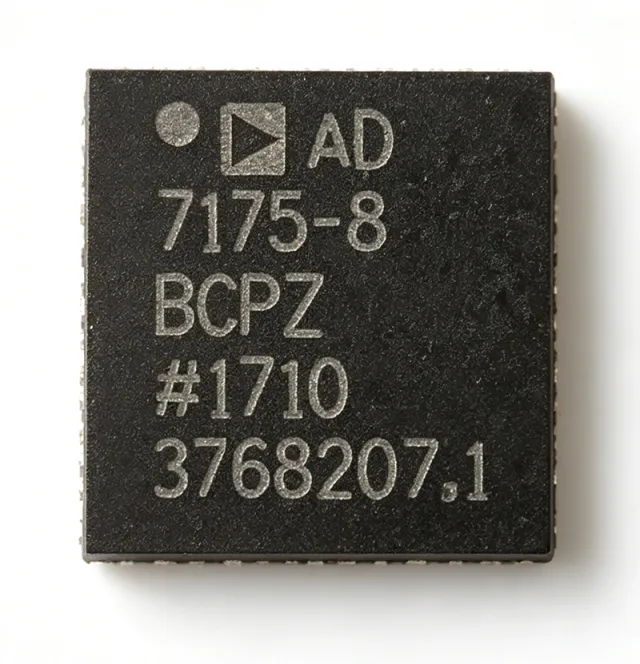
AD7175-8BCPZ-RL7 - 24-Bit Sigma-Delta ADC | Analog Devices
The AD7175-8BCPZ-RL7 is a low noise, fast settling, multiplexed, 8-/16-channel (fully/pseudo differential) sigma-delta analog-to-digital converter (ADC) from Analog Devices. It is designed for low bandwidth inputs and offers a maximum output data rate of 250 kSPS. The device integrates key analog and digital signal conditioning blocks, allowing users to configure an individual setup for each analog input channel in use. Each feature can be user selected on a per-channel basis. Integrated true rail-to-rail buffers on the analog inputs and external reference inputs provide easy-to-drive high impedance inputs. A sigma-delta ADC is a type of analog-to-digital converter that uses oversampling and noise shaping to achieve high resolution. It is part of the ADC family, which falls under data converters, a subset of analog-to-digital conversion in the broader category of mixed-signal ICs. Sigma-delta ADCs are known for their excellent linearity and low noise, making them ideal for precision measurement applications. Key features of the AD7175-8 include 24-bit resolution, 8 differential or 16 single-ended inputs, and a maximum output data rate of 250 kSPS. It operates from a 2.5 V to 5.5 V analog supply and a 2.3 V to 5.5 V digital supply. The device offers a programmable digital filter, allowing trade-offs between output data rate and noise. It also includes a 24-bit sigma-delta modulator, a digital filter, and a serial interface that supports SPI. The AD7175-8 is available in a 40-lead LFCSP-WQ (6x6 mm) package, which is RoHS3 compliant and has an MSL rating of 3 (168 hours). The AD7175-8 uses a high-performance sigma-delta architecture with a digital filter that can be configured for various output data rates and settling times. The device includes a multiplexer that allows up to 16 single-ended or 8 differential inputs. It also features an internal oscillator, eliminating the need for an external clock. The ADC provides a 24-bit output with a noise-free resolution of up to 24 bits at low data rates. The device is specified for operation over the industrial temperature range of -40°C to +105°C. Typical applications for the AD7175-8 include process control, industrial automation, temperature and pressure measurement, and precision data acquisition systems. Its high resolution and low noise make it suitable for applications requiring accurate measurement of slow-changing signals. The device is also used in weigh scales, medical instrumentation, and energy monitoring. When designing with the AD7175-8, it is important to provide adequate decoupling on the power supply pins and to use a clean analog ground plane. The reference inputs should be driven by a low-impedance source to maintain accuracy. The SPI interface should be isolated from noisy digital circuitry to prevent noise coupling into the analog section.