Interface ICs
ژێرپۆلەکان
بەرهەمەکان (5,100+)

AD9841JST - 20 MSPS CCD Signal Processor | Analog Devices
The Analog Devices AD9841JST is a 20 MSPS CCD signal processor packaged in a 48-pin LQFP measuring 7 mm by 7 mm. It belongs to the sensor and detector interface IC category, where signal-processing ICs convert analog sensor outputs into digital data for downstream acquisition, imaging, and control systems. The manufacturer has renamed the AD9841 to the AD9841A, so engineers evaluating new designs should review the current AD9841A documentation before finalizing a component specification. A CCD signal processor is a specialized interface IC that performs the timing, control, analog-to-digital conversion, and digital-processing functions required to read charge-coupled-device outputs. Such devices reduce the number of separate components required around a CCD sensor and help synchronize pixel-data transfer with downstream digital circuitry. The AD9841JST is identified specifically as a 20 MSPS CCD signal processor, making its headline performance figure the conversion or processing rate used when designing acquisition channels. The AD9841JST is offered in an LQFP-48 package. Its 7 mm by 7 mm footprint provides a practical surface-mount option for compact imaging boards, laboratory instruments, industrial cameras, and embedded optical systems. Because it is a legacy-specific ordering code, engineers should verify availability, lifecycle status, pin assignments, clocking requirements, and recommended operating conditions against the Analog Devices AD9841A product page and the appropriate technical documentation before releasing a production BOM. The manufacturer’s renaming notice is an important product-lifecycle consideration. The AD9841JST identifies the original AD9841 device, while AD9841AJSTZ is the related A-version ordering code identified in distributor records. Existing equipment maintenance and industrial product programs may need the original ordering code for exact-form-fit-function continuity, whereas new designs should determine whether the renamed AD9841A family provides a supported procurement path. AD9841-family devices are associated with CCD signal processing and are used when an imaging system requires coordinated sensor readout and digital conversion functions. Potential application areas include machine-vision cameras, semiconductor inspection equipment, scientific imaging instruments, barcode and document scanners, and other systems that digitize CCD output. Actual suitability depends on the sensor timing, analog input bandwidth, clock rate, power requirements, and digital interface configuration of the complete design. The principal design task is to match the signal chain rather than treat the device as a generic ADC. CCD outputs, bias levels, reset timing, channel count, and required data format must be compared with the device architecture before schematic capture. PCB planning should preserve short analog paths, provide a stable clock and supply reference environment, and keep high-speed digital outputs properly terminated. Use the package pin description and application information in the manufacturer documentation when assigning every signal and power pin. This product page combines the confirmed 20 MSPS classification, 48-LQFP package information, lifecycle-renaming context, and package-aware replacement analysis. It also identifies where a current equivalent or successor should be reviewed and provides engineering guidance for evaluating a signal-processing IC without assuming that a similar package number alone guarantees pin-to-pin compatibility.

AD9847KST - 10-Bit 40 MSPS CCD Processor | Analog Devices
The Analog Devices AD9847KST is a 10-bit, 40 MSPS CCD signal processor with an integrated programmable timing driver, operating from a 3 V or 5 V supply. It combines a complete analog front end and A/D conversion path for digital still-camera CCD imaging, with timing-clock adjustment at approximately 500 ps resolution. The device integrates the functions normally distributed across a CCD output amplifier, analog-to-digital converter, and external timing generator. A CCD signal processor is an imaging IC that conditions analog pixel charges and converts them into digital words while also generating the multi-phase clocking required by the image sensor. In the hierarchy of semiconductor components, the AD9847 belongs to the CCD signal processor and sensor-interface class, which is part of the broader analog front end and integrated-circuit category. Its integrated architecture reduces interconnections between the CCD output, converter, and timing circuitry while simplifying system-level image acquisition. Principal features include 10-bit quantization, a maximum conversion rate of 40 MSPS, operation from 3 V or 5 V, and programmable timing control with approximately 500 ps adjustment resolution. The timing-driver capability allows the sensor clock phases to be positioned accurately enough for high-speed pixel-transfer operations. The consolidated signal chain also reduces the number of external components required around a CCD output stage. Technically, the AD9847 divides the imaging interface into three closely coupled functions: analog CCD-signal conditioning, 10-bit digital conversion, and programmable timing generation. The approximately 500 ps timing resolution supports precise control of high-speed clocks at 40 MHz. This integration is especially useful when the design must transfer successive image rows while maintaining repeatable timing relationships between the sensor and sampling circuitry. Typical applications include digital still cameras, CCD-based imaging modules, industrial optical inspection systems, scientific cameras, and embedded vision equipment. In each case, the integrated timing driver can simplify clock generation while the 10-bit, 40 MSPS conversion path captures rapidly arriving analog pixel signals. Designers should still verify sensor timing, voltage levels, and output-noise requirements against the individual CCD and system requirements. For layout, keep analog input routing compact and place decoupling capacitors close to the supply pins. Treat the AD9847 timing outputs and analog input section as sensitive high-speed paths, with impedance-controlled routing and a quiet return path. Verify the final clock sequence, converter timing, and sensor voltage levels on hardware rather than relying only on nominal timing values. This page consolidates the manufacturer's key AD9847 specifications, application guidance, sourcing information, and replacement constraints into a design-focused reference. It also distinguishes documented device characteristics from parameters that require confirmation in the manufacturer datasheet, helping engineers plan CCD front-end development without relying on isolated distributor summaries.

AD9895KBC - 12-Bit CCD Signal Processor AFE | Analog Devices
The Analog Devices AD9895KBC is a highly integrated CCD signal processor for digital still camera applications, combining a complete analog front end and A/D conversion with a programmable timing generator. It is a 12-bit interface IC with logic input and logic output, packaged in a 64-CSPBGA package measuring 9 mm by 9 mm. According to the Analog Devices product page, the AD9895 and AD9891 use a Precision Timing core that provides 1 ns clock-adjustment resolution at 20 MHz operation and 700 ps resolution at 30 MHz operation. What is a CCD signal processor? A CCD signal processor is an interface and control IC designed to receive analog charge from a charge-coupled device, condition that signal, perform analog-to-digital conversion, and generate the timing required by the image sensor. In the broader electronics hierarchy, it is an interface IC, analog front end, and image-sensor signal-chain component. Combining the analog front end, converter, timing generator, and programmable timing control simplifies the design of digital camera systems compared with separate sensor-interface and timing blocks. Key features of the AD9895KBC include its 12-bit A/D conversion, programmable gain, ESD protection, logic-level input and output interfaces, and programmable timing generation. The timing core supports fine adjustment of high-speed clocks, with different stated resolution at 20 MHz and 30 MHz operating points. These characteristics make the device relevant to CCD-based imaging systems requiring coordinated sensor timing, signal conversion, and programmable analog control. The AD9895 architecture is intended for high-speed image-signal acquisition. Its integrated analog front end handles the sensor-side signal path, while the timing generator coordinates the required clock phases and reset levels. The programmable gain function provides an additional degree of control for matching the analog signal to the converter range. For camera designers, the central design consideration is preserving signal integrity across the CCD output, analog input, reference, clock, and digital interface networks while meeting the timing requirements of the target imaging sensor. Typical applications include digital still cameras, CCD imaging modules, professional camera systems, and embedded vision equipment that uses compatible CCD sensors. The same integration can reduce board area and the number of separately coordinated timing components, although system-level timing, grounding, decoupling, and clock-layout decisions remain essential. The 64-CSPBGA package is compact but uses a fine-pitch land pattern and requires careful PCB assembly and thermal management. For robust implementation, follow the Analog Devices AD9895 datasheet for the complete pin description, recommended power-supply connections, bypass-capacitor values, clocking limits, and timing-generator configuration. Verify the sensor-specific vertical and horizontal timing sequences, analog input range, reference-voltage requirements, and allowable operating temperature before releasing a production layout. This page combines the manufacturer product description, exact package and pricing references, verified replacement candidates, and practical integration guidance for engineers evaluating the AD9895KBC in CCD-based imaging equipment.

AD9943KCP - 10-Bit 25 MHz CCD Signal Processor | Analog Devices
The Analog Devices AD9943KCP is a complete 10-bit, 25 MHz single-channel CCD signal processor in a 32-LFCSP-WQ package measuring 5 mm by 5 mm. The device combines a correlated double sampler, programmable gain, 10-bit ADC, and digital processing functions for conditioning charge-coupled device outputs. Its 25 MHz analog sampling rate, 10-bit conversion resolution, and integrated signal-chain architecture make it suitable for compact imaging systems requiring high integration. A CCD signal processor is a specialized interface and data-conversion IC that conditions the relatively small analog charge signals produced by CCD imaging arrays. It converts those signals into digital words while handling pedestal subtraction, gain control, filtering, and related functions. Within the product hierarchy, the AD9943KCP belongs to the CCD signal-processor family, analog signal-processing ICs, interface ICs, and ultimately the broader semiconductor category. Principal features include a complete 10-bit, 25 MHz signal-processing architecture and an integrated analog front end. The 25 MHz operating rate supports high-frame-rate CCD imaging, while the 10-bit ADC resolution balances data-path precision with output size and bandwidth. The single-channel architecture targets interlaced and progressive-scan CCD arrays according to the Analog Devices product documentation. A 3 V supply is also identified for this device family. Technically, the AD9943KCP places multiple CCD-interface functions into one signal-chain IC rather than requiring separate amplifiers, sampling circuits, and conversion stages. This integration reduces external component count and board area, but the analog input path remains sensitive to layout quality. High-speed clocks, CCD outputs, reset timing, reference connections, digital outputs, and power-supply return paths require deliberate partitioning around the device. Typical applications include scientific and industrial CCD cameras, machine-vision equipment, imaging instruments, barcode and optical-inspection systems, and surveillance cameras. The part is particularly appropriate when a design needs a dedicated 10-bit CCD front end operating at 25 MHz without implementing a discrete correlated-double-sampling signal chain. PCB implementation should prioritize short CCD-output traces, continuous ground planes, symmetrical clock routing, and careful isolation of analog inputs from fast digital signals. Decoupling capacitors should be placed directly beside the corresponding supply and ground pins, while the exposed-pad thermal strategy must follow the package recommendations in the manufacturer datasheet. This product page combines the manufacturer specifications, a practical component-level comparison, drop-in alternatives, application guidance, and design notes to support faster engineering evaluation. Engineers should still validate timing, signal integrity, thermal performance, and production suitability using the Analog Devices datasheet and the intended CCD-array evaluation board.
AD9944KCP 12-Bit 25 MHz CCD Signal Processor | Analog Devices
The Analog Devices AD9944KCP is a complete 10-bit and 12-bit, 25 MHz CCD signal processor designed for high-speed imaging systems. It operates from a single 3 V power supply, typically dissipates 79 mW, and is packaged in a 32-lead LFCSP with a 5 x 5 mm footprint. The device combines analog CCD front-end processing, digital correction, programmable timing, and 12-bit signal-chain functionality for compact camera and video systems. A CCD signal processor is an integrated analog front-end and timing controller used to extract image information from charge-coupled-device sensors. The AD9944KCP belongs to the sensor and detector interface category, where it conditions the CCD output, applies gain and offset correction, and provides the digital interface required by downstream image-processing electronics. This integration reduces the number of discrete components required in a CCD imaging chain while supporting portable and space-constrained equipment. Key features include complete 10-bit and 12-bit operation, a 25 MHz processing capability, single 3 V operation, and typical power dissipation of 79 mW. The device is specifically intended for digital still cameras, digital video camcorders, PC cameras, portable CCD imaging devices, and CCTV cameras. Its integrated processing architecture allows the sensor output to be conditioned close to the image sensor, where shorter analog paths can reduce implementation complexity and improve system consistency. The AD9944KCP is offered in a 32-lead LFCSP package, identified in the product information as QCC32 and LFCSP-32 with a 5 x 5 mm body and exposed-pad construction. The 3 V supply requirement supports portable imaging systems where low-voltage operation and low power consumption are important. The manufacturer describes the AD9943 and AD9944 as a common signal-processing family with typical dissipation of 79 mW, making the family suitable for compact camera modules and portable CCD imaging devices. Typical applications include digital still cameras, digital video camcorders, PC cameras, portable CCD imaging devices, and CCTV cameras. In these systems, the device can process CCD timing and analog output information before data is transferred to a camera controller or image processor. The correct choice of timing, input, output, and power connections depends on the CCD sensor interface and the system clocking requirements, so the manufacturer data sheet should be used to implement the reference circuit and pin assignments. A key design consideration is the exposed thermal pad and the high-speed nature of the signal path. Follow the manufacturer’s recommended decoupling, grounding, and layout guidance, and confirm that the PCB land pattern and exposed-pad connection match the 32-lead LFCSP package. Verify the sensor timing, reset levels, and required external components against the AD9944 data sheet before production release. This page organizes the AD9944KCP’s identification, pricing, package information, application fit, and engineering guidance into a concise purchasing and design reference for engineers evaluating CCD signal-processing front ends.
AD9945KCP - 12-Bit 40MHz CCD Signal Processor | Analog Devices
Analog Devices AD9945KCP is a complete 12-bit, 40 MHz single-channel CCD signal processor housed in a 32-LFCSP-WQ 5 mm × 5 mm package. It combines a correlated double sampler, digitally controlled variable gain amplifier, black-level clamp, and 12-bit ADC in one analog front end optimized for interlaced and progressive-scan area CCD arrays. A CCD signal processor is an integrated analog front end that conditions the charge or voltage information produced by imaging arrays before digital conversion. Within the broader semiconductor hierarchy, the AD9945 is a sensor and detector interface IC, an analog front end, and a specialized data-conversion device. Its integrated signal chain reduces the number of separate analog conditioning stages required between a CCD output and an imaging system’s digital processing circuitry. The AD9945KCP supports sampling at up to 40 MHz and produces 12-bit digital output data. Its signal chain includes a correlated double sampler for extracting image information from CCD charge packets, a digitally controlled VGA for gain adjustment, and a black-level clamp for establishing the reference level used in image processing. The device also includes programmable gain, power-on reset, and automatic calibration functions identified in the AD9945KCP product description. The single-channel architecture is intended for systems that sample one CCD analog output at a time. It is particularly relevant to line-scan and area-array imaging systems operating with interlaced or progressive-scan CCDs. Integrating the sampling and gain-control functions directly in the signal processor helps designers establish a controlled analog path before the 12-bit conversion stage. Typical applications include industrial CCD inspection equipment, barcode and document scanners, machine-vision cameras, scientific imaging instruments, and optical metrology systems. The 40 MHz sampling capability supports high-speed image acquisition, while programmable gain and automatic calibration support repeatable operation across changing illumination or signal conditions. The 12-bit converter provides 4096 digital codes per sample. PCB design should prioritize short, controlled analog routing from the CCD output into the signal processor and away from high-speed digital and switching circuits. Use the manufacturer’s pin-description table and reference layout for the 32-LFCSP-WQ land pattern, exposed-pad connection, supply decoupling, and digital output routing. Verify thermal performance at the intended clock rate and output activity rather than relying only on nominal device specifications. This product page combines the AD9945KCP device identity, package information, functional block description, lifecycle positioning, drop-in replacement assessment, and practical design guidance. It also distinguishes directly interchangeable package variants from the broader class of functionally similar CCD signal processors that require design review.

AD9948KCP - 10-Bit 25 MSPS CCD Signal Processor | Analog Devices
Analog Devices AD9948KCP is a 10-bit CCD signal processor with a Precision Timing core, operating at pixel rates up to 25 MHz and packaged in a 40-LFCSP 6 mm × 6 mm package. The device integrates a programmable timing driver, a 10-bit analog-to-digital converter, and an analog signal-processing front end for digital still-camera imaging systems. A CCD signal processor is an interface IC that conditions charge-coupled device output signals and converts them into digital image data. In the electronic hierarchy, the AD9948 belongs to the sensor and detector interface family, where it connects an imaging sensor to a digital imaging pipeline. Its integrated Precision Timing core adjusts high-speed clocks with 800 ps resolution, while the analog front end handles correlated double sampling, gain, and black-level control. The principal specifications include a 10-bit conversion resolution, a maximum pixel rate of 25 MHz, and integrated analog-front-end functions. The front end includes an 18 dB pixel gain amplifier, a 10-bit variable gain amplifier, and a 10-bit 25 MSPS analog-to-digital converter. Black-level clamping and programmable timing capabilities reduce the number of external signal-conditioning functions required in a CCD imaging channel. Technically, the AD9948 combines the CCD analog front end, conversion circuitry, and clock-generation functions in one device. The Precision Timing core provides 800 ps clock-adjustment resolution for controlling high-speed imaging timing. This integration supports a compact implementation of digital still-camera signal chains while preserving programmable control over gain, offset, and clock timing. Exact voltage, power, temperature, and clock-output limits should be confirmed against the Analog Devices AD9948 data sheet before schematic release. Typical applications include digital still cameras, CCD-based imaging modules, industrial vision equipment, and scientific or medical imaging systems in which programmable timing and integrated signal conditioning are valuable. The device is particularly relevant where a CCD output must be amplified, clamped, digitized, and transferred to a camera processor without implementing each function as a separate circuit. Design work should preserve the separation required between sensitive CCD inputs and digital timing outputs, use controlled-impedance routing for high-speed signals, and decouple the analog and digital supplies near their respective pins. Component values, clock limits, and supply requirements should be copied directly from the manufacturer reference circuit and data sheet rather than inferred from generic CCD-interface designs. This page organizes the verified product identity, package, pricing evidence, technical capabilities, and sourcing details into one engineering-focused reference. It also distinguishes the exact AD9948KCP orderable part from related order codes and records where additional datasheet-level information is required for a final PCB or production design.
AD9949KCP - 12-Bit CCD Signal Processor | Analog Devices
The Analog Devices AD9949KCP is a 12-bit CCD signal processor with a programmable timing driver for digital still camera applications, operating at pixel rates up to 36 MHz and packaged in a 40-lead LFCSP with exposed pad. The integrated processor combines an analog front end, 12-bit A/D conversion, and Precision Timing core technology with clock adjustment resolution below 600 ps. A CCD signal processor is a specialized interface IC that conditions CCD output signals, converts them into digital data, and generates the precision timing signals required by an imaging sensor. In the product hierarchy, it belongs to sensor and detector interface ICs within integrated circuits. Combining the analog front end, converter, and timing driver reduces the number of separate timing and signal-conditioning elements required in a digital camera signal chain. Key features include a 12-bit conversion format, operation at pixel rates up to 36 MHz, and a programmable timing driver. The Precision Timing core allows adjustment of high-speed clocks with resolution below 600 ps. The analog front end also includes black-level clamping, while the integrated architecture supports compact digital still camera designs. These functions address amplitude correction, digitization, and sensor timing within one device. Technically, the AD9949 combines analog signal acquisition and digital conversion with deterministic timing generation in a single 40-lead LFCSP package. The 6 x 6 mm surface-mount construction supports compact camera modules, while the exposed pad provides a thermal and electrical connection to the PCB. The processor accepts CCD-derived analog information and produces digital output while coordinating high-speed sensor timing, reducing the complexity of separating those functions across multiple devices. Typical applications include digital still cameras, CCD imaging modules, and sensor-interface electronics requiring synchronized pixel clocks and digitized image data. Its 36 MHz pixel-rate capability is suited to digital camera signal chains, while the programmable timing core allows timing adjustments for sensor-system optimization. The 12-bit converter also provides sufficient resolution for many imaging paths where compactness and integrated timing control are priorities. Designers should preserve the exposed-pad connection beneath the LFCSP and use the manufacturer pin-description table when assigning PCB nets. Power, analog ground, digital ground, and high-speed timing connections require careful partitioning because signal integrity across the CCD interface directly affects conversion performance and clock alignment. This product page combines the manufacturer specifications with package details, sourcing guidance, replacement considerations, and practical interface-design notes. It also distinguishes the AD9949KCP from documented AD9949-family ordering variants by package, temperature marking, and production status, helping engineers choose the correct exact MPN before placing a design into production.

AD9991KCP - 10-Bit CCD Signal Processor | Analog Devices
Analog Devices AD9991KCP is a 10-bit CCD signal processor with a precision timing generator, combining an analog CCD front end, 10-bit variable gain amplifier, 10-bit A/D converter, correlated double sampling, black-level clamp, and programmable timing control in a 56-lead LFCSP-VQ package. The device supports 4-phase and 6-phase vertical clocking, uses a 27 MHz A/D converter, and provides precision timing adjustment with 800 ps resolution. A CCD signal processor is an integrated interface IC that conditions analog pixel signals and manages the clocks required to transfer charge through a charge-coupled device. In the electronic hierarchy, it belongs to interface ICs and sensor-detector interfaces. Its purpose is to translate a CCD output into a digitized, gain-controlled image signal while synchronizing horizontal and vertical transfer clocks with the imaging system. The AD9991 combines a 10-bit variable gain amplifier, correlated double sampling, black-level clamp, and a 10-bit 27 MHz A/D converter. It supports both 4-phase and 6-phase vertical transfer clocks. The programmable timing generator can adjust high-speed clocks with 800 ps resolution, helping camera and imaging designers establish repeatable pixel timing without implementing a separate timing-control system. Its integrated architecture reduces the number of discrete analog and digital blocks required around a CCD. Correlated double sampling rejects much of the reset noise present in CCD pixel output, while the variable gain amplifier accommodates different scene illumination levels. The 10-bit converter provides 1,024 quantization levels for the digitized analog signal, and the black-level clamp helps establish a stable black reference before image processing. The AD9991 was designed for digital still cameras and camcorders, where CCD sensors require coordinated transfer clocks, analog gain control, black-level correction, and high-speed digitization. The same signal chain can support industrial imaging, barcode-scanning optics, machine-vision cameras, and other CCD-based systems when their sensor timing and electrical requirements are compatible with the device. PCB implementation requires careful attention to the 56-lead LFCSP-VQ footprint, exposed-pad thermal design, analog input routing, and clock-signal integrity. Follow the manufacturer datasheet for the complete pin-description table, recommended decoupling, clock-generation settings, and exposed-pad land pattern. Verify sensor timing, serial interface mode, operating supply rails, and digital I/O levels before finalizing a new design. This page combines the core AD9991KCP specifications, a source-linked datasheet reference, practical application guidance, and a package-compatible replacement assessment. It also distinguishes the KCP ordering code from the related KCPZ and KCPZRL variants so engineers can review temperature, packaging, and qualification requirements before committing a legacy imaging design to procurement.
AD9995KCP - 12-Bit 36 MHz CCD Signal Processor | Analog Devices
Analog Devices AD9995KCP is a highly integrated 12-bit CCD signal processor with a precision timing generator, designed for digital still-camera and camcorder imaging systems. The device combines a complete analog front end and analog-to-digital conversion function with programmable CCD timing generation in a 56-lead LFCSP package, and its converter operates at up to 36 MHz. Its integrated signal chain supports six-phase vertical transfer clock generation, correlated double sampling, a 10-bit variable gain amplifier, a 12-bit A/D converter, and a black-level clamp. A CCD signal processor is an interface IC that sits between a charge-coupled-device image sensor and the downstream digital image-processing system. It conditions the small, noisy analog pixel signal, performs correlated double sampling, applies programmable gain and black-level correction, converts the conditioned signal to digital data, and generates the clocking required to transfer and read the CCD. In the broader hierarchy, the AD9995KCP belongs to the sensor and detector interface class of integrated circuits. The principal benefit of this integration is reduced external circuitry and a more compact camera electronics architecture. Instead of separately implementing analog front-end conditioning, pixel conversion, and CCD clock generation, a camera designer can use one highly integrated device. The 36 MHz conversion capability supports high-rate pixel readout, while the six-phase timing generator simplifies operation of CCDs that require multiple vertical transfer phases. The analog front end uses correlated double sampling to reduce reset noise and source-fanout noise in CCD pixel outputs. Its 10-bit variable gain amplifier provides adjustable signal conditioning before digitization, and the black-level clamp establishes a stable pedestal reference for the converted image data. The 12-bit A/D converter preserves more quantization levels than a 10-bit signal chain, supporting smoother luminance transitions and more detailed digital-image representation when the remaining analog and optical errors are properly managed. Typical uses include digital still cameras, camcorders, surveillance cameras, machine-vision cameras, and other CCD-based imaging products. In these systems, the AD9995KCP can manage sensor-side timing, recover weak pixel voltages, apply gain and pedestal correction, and deliver parallel digital pixel data to an image processor. Its integration is particularly useful when board area, component count, and predictable sensor timing are priorities. Designers should treat the 56-lead LFCSP as a high-speed mixed-signal layout challenge. The analog input path, converter, clock outputs, digital data outputs, power distribution, and exposed-pad thermal path require careful plane partitioning and short return paths. Use the manufacturer's pin description table for exact signal assignments and the application information for recommended external components. Camera-system validation should also include optical black pixels, gain calibration, timing sequencing, and image-noise testing because those outcomes depend on the CCD, lens, sensor interface, and downstream processing as well as on this IC. This page combines the documented AD9995KCP function set with exact-package sourcing information, practical integration guidance, and qualified drop-in alternatives. It focuses on the decisions that matter when integrating a 36 MHz, 12-bit CCD signal processor into compact imaging equipment, including timing architecture, analog conditioning, package handling, and replacement risk.

ADG1204YCPZ-500RL7 - ±15V/+12V 4:1 iCMOS Multiplexer, 12-LFCSP
The Analog Devices ADG1204YCPZ-500RL7 is a monolithic CMOS analog multiplexer comprising four single channels in a 4:1 (SP4T) configuration, built on Analog Devices' iCMOS (industrial CMOS) modular process that combines high-voltage CMOS with bipolar technologies. The device operates from a single analog supply of ±15 V or +12 V dual analog rails, with rail-to-rail signal handling and 3 V logic-compatible digital inputs, eliminating the need for a separate VL supply rail. Housed in a 12-lead LFCSP (3x3 mm) package with an exposed pad, it delivers an on-resistance of 190 Ω typical and ultra-low 1.5 pF off source capacitance. An analog multiplexer (mux) is a precision solid-state switch that routes one of multiple analog input channels to a common output under digital control. Within the broader signal-chain hierarchy, an analog mux sits between the analog front end (sensors, instrumentation amplifiers) and the data converter (ADC), occupying the same functional niche as a relay matrix but with orders-of-magnitude faster switching and no mechanical wear. Multiplexers like the ADG1204 trade raw RF bandwidth for very high DC accuracy and charge-injection performance, which is why they dominate precision data-acquisition and sample-and-hold front ends. Key features include <1 pC charge injection when switching channels (critical for glitch-free sample-and-hold), 33 V maximum supply range, fully specified rail-to-rail operation, fully specified ±15 V/+12 V performance, and 3 V logic-compatible inputs that interface directly to modern FPGAs and microcontrollers without level shifters. iCMOS construction ensures ultralow power dissipation in a footprint compatible with portable instrumentation. The exposed pad of the LFCSP-12 package provides a low-thermal-resistance path to PCB copper, supporting reliable operation across the -40 °C to +125 °C automotive/industrial temperature range. Architecturally, the ADG1204 uses four independent NMOS transmission gates with break-before-make switching and TTL/CMOS-compatible address logic. The sub-1 pC charge injection is achieved through a proprietary switch-driver topology that cancels the gate-drain overlap charge, making the device suitable for sample-and-hold applications where channel-to-channel switching transients would otherwise corrupt the held voltage. Typical applications include precision data acquisition front ends, sample-and-hold amplifiers, automated test equipment (ATE) channel selection, audio/video signal routing, and battery-powered instrumentation where the iCMOS low-power advantage matters most. The 3x3 mm LFCSP footprint also makes it a strong fit for space-constrained multi-channel designs. When designing with the ADG1204, observe that the on-resistance of 190 Ω is not constant across the signal range - it varies with VDS and is highest near the rails. For low-distortion audio applications, keep signal amplitudes within ±5 V of mid-supply where RON flatness is best. The exposed pad must be soldered to a sufficient ground plane to keep junction temperature within spec; thermal vias to internal ground layers are strongly recommended. This page synthesizes distributor pricing, drop-in alternatives, and practical design notes not found in the manufacturer datasheet alone.
ADG1204YCPZ-REEL7 - ±15V 4:1 iCMOS Mux, 190Ω, 12-LFCSP | ADI
The Analog Devices ADG1204YCPZ-REEL7 is a low-capacitance, low-charge-injection, monolithic CMOS analog multiplexer configured as a 4:1 single-pole four-throw (SP4T) switch, with an on-resistance of 190 Ω and packaged in a 12-lead LFCSP (3 mm × 3 mm). It operates from dual ±15 V supplies or a single +12 V supply, making it suitable for industrial analog signal chains where bipolar headroom is required. An analog multiplexer (MUX) is a semiconductor switch that routes one of multiple analog input signals to a common output line under digital logic control, and it sits within the broader category tree of analog switch -> multiplexer/demultiplexer -> interface IC -> integrated circuit. The ADG1204 uses ADI's iCMOS (industrial CMOS) process, which combines high-voltage CMOS and bipolar transistors on a single die to deliver ±15 V signal swings with the low power dissipation typical of CMOS logic. Key features include ultralow charge injection (typically < 1 pC), low on-capacitance for minimal signal distortion at high frequency, fast switching speed with a bandwidth suitable for video signals, and a break-before-make action that eliminates momentary shorting between adjacent channels. The digital interface accepts standard TTL/CMOS logic levels at the A0 and A1 address pins plus an active-low EN to put the device into a high-impedance state when disabled. Architecturally, the ADG1204 integrates four independent n-channel MOSFET pass gates whose sources connect to the common D pin and whose drains terminate at the four S1–S4 pins, with logic translation circuitry ensuring that 3 V microcontroller GPIO can reliably drive the part from ±15 V analog rails. The iCMOS process also enables latch-up immunity under over-voltage transients. Typical applications include data-acquisition front ends, sample-and-hold circuits, video signal routing, ATE (automatic test equipment) pin switching, and precision instrumentation multiplexers. The wide supply tolerance allows direct interfacing to ±12 V or ±15 V op-amp outputs in industrial control loops. When designing with this device, ensure logic levels at the address pins remain within 0 V to VDD regardless of analog signal swing, and place 0.1 µF decoupling capacitors as close as possible to each supply pin. The exposed pad on the LFCSP package must be soldered to the PCB ground plane to achieve the rated power dissipation and to maintain the specified on-resistance stability. This page synthesizes distributor pricing, drop-in pin-compatible alternatives, and practical PCB design notes not found in the standalone ADI datasheet.
ADG1206YCPZ-REEL7 - 16:1 iCMOS Mux, Low Cap, ±15V/12V | ADI
The Analog Devices ADG1206YCPZ-REEL7 is a monolithic iCMOS analog multiplexer that switches one of sixteen inputs to a common output, controlled by 4-bit binary address lines A0, A1, A2, and A3, and is housed in a 32-lead LFCSP-WQ (5 mm × 5 mm) package with on-resistance of 200 Ω maximum. It is built on Analog Devices' iCMOS process technology, which combines high-voltage CMOS, bipolar, and DMOS elements to deliver ±15 V / +12 V dual supply operation with ultralow power dissipation and ESD protection. The part is supplied on a 7-inch reel (-REEL7) and is specified over the -40 °C to +125 °C extended industrial temperature range. A multiplexer (MUX) is a switching component that selects one of multiple analog input signals and forwards the chosen channel to a single output line, controlled by a digital address. MUX devices sit within the broader signal-chain hierarchy: analog switch → multiplexer → data-acquisition front-end → mixed-signal subsystem. The 16:1 configuration implemented in the ADG1206 is the single-ended counterpart to the differential 8:1 ADG1207, both built on the same iCMOS die family. Key specifications include 200 Ω on-resistance (max), 13 pF typical on-capacitance, 490 MHz -3 dB bandwidth, 75 ns tON / 85 ns tOFF transition times, and ±15 V or +12 V single-supply operation. Ultralow charge injection (typically <1 pC) and low parasitic capacitance make it well-suited for data-acquisition front-ends, sample-and-hold circuits, and precision instrumentation where minimal signal-glitch and fast settling are required. The LFCSP-WQ-32 package includes an exposed thermal pad that must be soldered to the PCB ground plane for proper thermal and electrical performance. The iCMOS architecture allows ±15 V analog signal swings while running from a low-voltage logic interface, eliminating the need for external level shifters. The latch-up-immune construction and ESD robustness exceed 4 kV HBM on the analog inputs, making the part tolerant of harsh industrial environments. Designers should note that the ADG1206YCPZ-REEL7 and the ADG1206YCPZ (tray) are the same die in different packaging media; the only difference is the carrier format (reel vs. tray) for high-volume assembly. Typical applications include automated test equipment (ATE) and switching matrices, data-acquisition systems, sample-and-hold amplifiers, medical imaging front-ends, communication system routing, and avionics signal multiplexing. The wide analog signal range and low distortion also suit audio routing and video switching designs. For battery-powered or precision portable instruments, the ultralow power dissipation (typically <0.5 µW quiescent) extends operating life. A key design consideration is the analog ground (AGND) and digital ground (DGND) pin arrangement: the LFCSP-WQ-32 package provides separate analog and digital ground pins that should be tied to a low-impedance ground plane to minimize crosstalk between the digital address lines and the analog signal path. Designers must also observe the absolute maximum analog input voltage of ±25 V with respect to AGND, even when the supplies are off, to avoid latch-up. This page synthesizes manufacturer datasheet parameters, distributor pricing as of 2026-10-06, drop-in cross-references, and practical design notes not consolidated in any single vendor listing, providing unique value beyond Digi-Key or Mouser product pages.
ADG1207YCPZ - Low Cap 8-Ch ±15V iCMOS Mux | Analog Devices
The Analog Devices ADG1207YCPZ is a monolithic iCMOS analog multiplexer integrating eight differential channels in a 32-lead LFCSP-WQ (5x5 mm) package with 200 ohm on-resistance and ultra-low 1.5 pF off capacitance. It switches one of eight differential inputs to a common differential output, addressed by a 3-bit binary code on A0, A1, and A2, and operates from dual ±5 V to ±15 V supplies or a single 12 V supply with up to 33 V total range. An analog multiplexer (mux) is a semiconductor switch that routes one of multiple analog input signals to a single output line under digital control, forming the front-end of a data acquisition system. In the hierarchy of signal-chain components, the mux sits between sensors or transducers and downstream amplifiers or converters, and as a member of the analog switch IC family it is valued for low on-resistance, low capacitance, and fast settling. The ADG1207 belongs specifically to the iCMOS process family, which combines high-voltage CMOS with sub-micron logic to achieve low power and small footprint simultaneously. Key differentiating features include less than 1 pC charge injection over the entire signal range, rail-to-rail signal handling, break-before-make switching action that prevents momentary shorting between channels, and TTL/CMOS-compatible 3 V logic inputs that interface directly to modern microcontrollers and FPGAs. The wide 33 V supply range supports industrial ±15 V systems as well as single-supply 12 V designs, and the 200 ohm on-resistance remains flat across the signal range, minimizing distortion in precision paths. The device uses iCMOS construction, an Analog Devices process technology that places a high-voltage analog transistor layer on top of a sub-micron CMOS logic layer. This allows the analog switches to handle ±15 V signals while the address decoders operate at sub-5 V CMOS levels, achieving ultralow power dissipation and latch-up immunity in a compact surface-mount package. Typical applications include data acquisition front-ends, sample-and-hold circuits, automatic test equipment (ATE) signal routing, audio and video signal switching, battery-powered instrumentation, and avionics multiplexing. The differential 8:1 architecture is particularly suited for balanced signal chains such as professional audio, instrumentation amplifiers, and isolated ADC front-ends where common-mode rejection matters. When designing with the ADG1207YCPZ, ensure the address lines are stable before VDD ramps to avoid parasitic channel selection during power-up, and place 100 nF decoupling capacitors close to each supply pin. For highest DC accuracy in low-impedance loads, select the ADG1407 family instead, since the ADG1207's 200 ohm on-resistance dominates error in sub-kohm paths. This page synthesizes distributor pricing, verified drop-in alternatives, and practical design notes not found in the standalone datasheet, giving engineers a single source for selection, sourcing, and layout guidance.

ADG1208YRUZ-REEL7 - 8:1 iCMOS MUX, 16-TSSOP | Analog Devices
The Analog Devices ADG1208YRUZ-REEL7 is a monolithic, single 8-to-1 analog multiplexer built on Analog Devices' iCMOS (industrial CMOS) process, packaged in a 16-pin TSSOP (YRU) with a 200 ohm on-resistance. It switches one of eight analog inputs to a common output as determined by 3-bit binary address lines A0, A1, and A2, operating from dual +/-5 V to +/-15 V supplies or a single +12 V supply across a 33 V supply range. An analog multiplexer is a semiconductor switch that routes one of multiple analog input signals to a single output line under digital control. MUXes belong to the broader category of analog switches and multiplexers, which sit under interface ICs and are essential building blocks in data acquisition (DAQ), instrumentation, audio routing, and automatic test equipment (ATE). The ADG1208's iCMOS process combines high-voltage CMOS with submicron CMOS, providing low power consumption, low on-resistance, and high switching speed in a small footprint. Key features include 200 ohm on-resistance (160 ohm per third-party sources), 5 ohm on-resistance flatness, +/-15 V dual supply operation, 1 pC charge injection, 2 pF off capacitance, 75 dB off-isolation, and 60 ns transition time. The device also offers break-before-make switching, rail-to-rail operation, 3 V logic-compatible digital inputs, and fully specified performance with +/-5 V, +5 V, +/-12 V, or +12 V supplies. The ADG1208 employs parallel CMOS switches with parasitic-junction-isolated bodies, enabling low charge injection and low capacitance. The wide supply range supports industrial signal levels up to +/-15 V while the 3 V logic interface allows direct connection to modern microcontrollers, FPGAs, and ADCs without level shifters. Typical applications include data acquisition front-ends, sample-and-hold systems, PLC analog input modules, ATE signal routing, audio/video signal switching, and battery-powered instrumentation. The TSSOP-16 footprint suits space-constrained PCB designs. When designing with the ADG1208, add 0.1 uF bypass capacitors near each supply pin and ensure unused digital address lines are tied to GND or VDD to avoid floating-state channel selection. The break-before-make architecture prevents momentary shorting between channels during switching transitions. This page synthesizes verified distributor pricing, pin-compatible drop-in alternatives, and application-specific design guidance not consolidated in the manufacturer datasheet, providing an engineering decision aid for sourcing and design-in.
ADG1213YRUZ - Quad SPST iCMOS Switch, 120Ω, ±15V | Analog Devices
The Analog Devices ADG1213YRUZ is a monolithic iCMOS (industrial CMOS) quad SPST (Single-Pole Single-Throw) analog switch housed in a 16-pin TSSOP (YRU) package, featuring 1 pF off capacitance, 2.6 pF on capacitance, <1 pC charge injection, and 120 Ω on resistance. It operates from ±4.5 V to ±16.5 V dual supplies or up to +12 V single supply with rail-to-rail signal handling and 33 V maximum supply range. An iCMOS switch is a monolithic CMOS device that combines high-voltage CMOS and bipolar process steps, enabling analog switches that tolerate ±15 V supplies while still allowing 3 V logic-compatible control inputs without requiring a separate V_L rail. The ADG1211/ADG1212/ADG1213 family sits in the broader hierarchy of analog switches → multiplexers → signal-chain interface ICs → mixed-signal semiconductors, and serves as a precision, low-charge-injection building block between sensitive analog front ends and higher-voltage analog signal paths. Key differentiating features include four independently selectable normally-open SPST channels (the ADG1211 is normally-open, ADG1212 normally-closed, ADG1213 contains two of each - check device grade), sub-1 pC charge injection that minimizes transient switching disturbance on sample-and-hold capacitors, and typical power consumption below 0.03 µW, making it well suited for power-sensitive multi-channel instrumentation. The 120 Ω on resistance is fully specified at ±15 V and +12 V with a flat, low-distortion characteristic across the audio band. Architecturally, the ADG1213 leverages the iCMOS process to integrate high-voltage DMOS transistors alongside low-voltage CMOS logic on a single die, eliminating the need for a logic-level shifter supply and simplifying board-level power-tree design. Each switch is independently controlled by a TTL/CMOS-compatible digital input, and all four channels exhibit matched on-resistance and ton/toff timing for synchronized multi-channel sampling. Typical applications include precision data-acquisition front ends, audio and video signal routing, automated test equipment (ATE) multiplexers, medical instrumentation, communication systems, and battery-powered multi-channel sensor switching where charge injection and input capacitance directly affect measurement integrity. When designing with this device, place 0.1 µF or larger decoupling capacitors as close as possible to the VDD and VSS pins, and keep digital control traces isolated from analog signal paths to preserve the low charge-injection and low distortion performance. The TSSOP-16 footprint is compatible with ADG1211YRUZ and ADG1212YRUZ variants for design reuse across NC/NO options. This page synthesizes distributor pricing, drop-in alternatives, and practical design notes not found in the manufacturer datasheet, providing a single-source engineering reference for the ADG1213YRUZ.

ADG1219BRJZ-REEL7 - ±15V/12V iCMOS SPDT Switch SOT-23-8 | Analog Devices
The Analog Devices ADG1219BRJZ-REEL7 is a monolithic iCMOS SPDT (single-pole double-throw) analog switch housed in an 8-pin SOT-23 package, featuring an active-low EN input that simultaneously disables both channels. The device is fully specified at +12 V single supply and ±15 V dual supply rails, exhibits a low 200 ohm on resistance, less than 0.5 pC charge injection over the full signal range, and 2.5 pF off capacitance, making it well-suited for precision signal-chain switching in industrial and instrumentation systems. A SPDT (single-pole double-throw) analog switch is a fundamental building block of the analog switch and multiplexer family. It routes one input signal to one of two outputs, or vice versa, using MOSFET pass transistors controlled by a logic-level input. SPDT switches sit within the broader taxonomy of analog switches -> multiplexers -> interface ICs -> signal conditioning, where they are valued for their bidirectional signal paths, near-zero quiescent current, and ability to handle rail-to-rail analog signals. The iCMOS (industrial CMOS) process used in the ADG1219 allows high-voltage bipolar swings (±15 V / 12 V) on a monolithic CMOS die, combining low power consumption with the wide dynamic range traditionally reserved for junction-isolation processes. Key features that differentiate this part include break-before-make switching action that prevents momentary shorting between channels during transitions, a low 0.6 nA maximum off leakage current at 85 °C, and 3 V to 16.5 V single-supply operation without requiring a logic-level VL supply. The 2.5 pF off capacitance and sub-1 pC charge injection make the ADG1219 well matched to data-acquisition front ends where injected charge would otherwise corrupt sample-and-hold settling. Typical application circuits include audio signal routing, ATE (automatic test equipment) channel selection, video switching, precision data-acquisition multiplexers, and battery-powered instrumentation. The enable pin simplifies power-down sequencing in multi-channel systems, allowing designers to put unused switches into a high-impedance state with a single control line. When designing with this part, place 0.1 µF decoupling capacitors close to VDD and VSS pins to suppress logic-induced transients. Because the switch is bidirectional, source and drain terminals are interchangeable, simplifying PCB layout. For applications that exceed ±15 V signals, review the absolute maximum ratings in the manufacturer datasheet. This page synthesizes distributor pricing, drop-in alternatives, and practical design notes not found in the manufacturer datasheet alone.
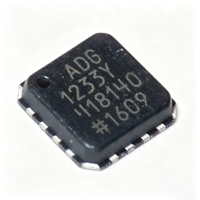
ADG1233YCPZ-REEL7 - Triple SPDT Analog Switch | Analog Devices
The ADG1233YCPZ-REEL7 is a monolithic iCMOS® analog switch from Analog Devices, integrating three independently selectable single-pole, double-throw (SPDT) switches in a compact 16-lead LFCSP-VQ (4x4 mm) package. It operates over a wide supply range of ±15 V or +12 V, with a low on-resistance of 120 Ω (typical) and ultra-low capacitance of 1.5 pF off capacitance, making it ideal for high-performance signal routing in precision instrumentation, audio, and data acquisition systems. An analog switch is a semiconductor device that selectively connects or disconnects an analog signal path under digital control. It is a fundamental building block in signal routing, multiplexing, and sample-and-hold circuits. The ADG1233 belongs to the family of analog switches and multiplexers, which are part of the broader category of interface ICs and signal conditioning components. Its iCMOS® (industrial CMOS) process technology ensures low power consumption and high voltage handling, bridging the gap between traditional CMOS and higher-voltage bipolar processes. Key features include break-before-make switching action, which prevents momentary shorting when switching channels, and an EN input that enables or disables the entire device. The switch is fully specified with 3 V logic-compatible inputs, allowing direct interface with low-voltage digital controllers. Rail-to-rail operation ensures minimal signal distortion across the full supply range. The 1.5 pF off capacitance and 0.5 pC charge injection minimize signal degradation in high-frequency and precision applications. The ADG1233 utilizes a proprietary iCMOS® process that combines the advantages of high-voltage CMOS with low power dissipation. This architecture enables the device to handle ±15 V supplies while maintaining low leakage currents and fast switching speeds. The break-before-make action is implemented through internal timing circuitry, ensuring reliable channel isolation during transitions. The device is available in a 16-lead LFCSP-VQ package, which offers excellent thermal performance and a small footprint for space-constrained designs. Typical applications include audio signal routing, precision data acquisition systems, automatic test equipment (ATE), and medical instrumentation. The low capacitance and charge injection make it particularly suitable for high-speed analog signals, while the wide supply range accommodates both bipolar and single-supply designs. The EN pin provides a convenient means of power-down or signal isolation in multi-channel systems. When designing with the ADG1233, ensure that the digital control signals are within the specified logic thresholds and that the supply voltages are properly decoupled with 0.1 µF capacitors close to the VDD and VSS pins. The break-before-make feature eliminates the need for external timing circuits, but the user should verify that the switching time meets system requirements.

ADG1236YCPZ-500RL7 - Dual SPDT ±15V iCMOS Analog Switch | ADI
The Analog Devices ADG1236YCPZ-500RL7 is a low-capacitance, low-charge-injection dual SPDT (single-pole double-throw) analog switch fabricated on the iCMOS process, offering a 33 V supply range, 1 pC charge injection, and 1.3 pF off capacitance in a 12-lead LFCSP (3 mm x 3 mm) package. An analog switch is an electronic component that routes or blocks analog signal paths under digital control. Within the signal-chain hierarchy, it belongs to the multiplexer/switch family of interface ICs, sitting between sensors or signal sources and amplifiers, ADCs, or measurement front ends. SPDT switches route one common terminal to one of two throw terminals, enabling source selection, gain-range switching, and redundant-path switchover in precision systems. Key features include 1.3 pF off capacitance and 3.5 pF on capacitance, which minimize signal distortion in high-frequency and capacitive-sensitive nodes, and 1 pC charge injection that reduces glitches when switching precision sample-and-hold or integrator circuits. The 33 V supply range supports +/-15 V dual-supply and 12 V single-supply operation, and the iCMOS process combines high-voltage CMOS and bipolar technologies for industrial-grade robustness. Logic inputs are 3 V logic-compatible and no VL supply pin is required, simplifying interfacing with low-voltage controllers. Technically, the iCMOS process allows high-voltage analog handling with low-voltage digital control, so the switch blocks up to +/-15 V signals while the control logic accepts standard 3.3 V or 5 V levels. The monolithic CMOS construction ensures low power and matched switch behavior across both SPDT channels, which switch independently for flexible routing. Typical applications include automated test equipment (ATE) signal routing, data-acquisition channel selection, precision sample-and-hold circuits, and industrial instrumentation where large-swing signals meet low-glitch switching requirements. Design consideration: on resistance is approximately 120 ohm typical (190 ohm maximum per DigiKey listing), so account for Ron flatness and voltage drop in high-impedance or precision-gain paths. This page synthesizes distributor pricing, drop-in alternative analysis, and practical design notes not found in the manufacturer datasheet, with data verified as of 2026-09-10.
ADG1408YRUZ - 8:1 CMOS Analog Multiplexer | Analog Devices
The Analog Devices ADG1408YRUZ is an 8:1 CMOS analog multiplexer with a maximum on-resistance of 4.7 ohms at 25°C, continuous current up to 190 mA, and 3 V-compatible logic inputs in a 16-lead TSSOP package. It switches one of eight inputs to a common output according to three binary address lines, A0, A1, and A2. An analog multiplexer is an analog switch network that connects one selected source channel to a shared destination. In the ADG1408, eight single-ended inputs are multiplexed onto one output. The address inputs control the selected path, while the common output provides a compact way to route signals in test equipment, data-acquisition systems, relay-replacement circuits, and audio/video equipment. This places the device in the interface IC hierarchy: analog switch → multiplexer → signal-routing IC. Key features include a maximum on-resistance of 4.7 ohms, on-resistance flatness of 0.5 ohm, rail-to-rail operation, and break-before-make switching. The manufacturer lists operation across ±15 V, +12 V, and ±5 V supplies, plus compatibility with 3 V logic inputs. These features make the ADG1408 suitable for systems that require controlled switching of bipolar or low-voltage signals while maintaining defined break-before-make behavior. The ADG1408YRUZ is specified in a 16-lead TSSOP package. Its 4.7-ohm maximum on resistance and 190-mA continuous-current capability provide useful performance for precision signal routing, although insertion loss and settling behavior depend on the source impedance, load, signal frequency, supply voltage, and layout. The 0.5-ohm on-resistance flatness helps minimize resistance variation across the selected switch network. Typical applications include relay replacement, audio and video routing, automatic test equipment, data-acquisition systems, and signal-path multiplexing. The break-before-make action is particularly useful where briefly connecting two externally driven sources is undesirable. For high-speed or high-impedance systems, engineers should evaluate switch capacitance, off leakage, charge injection, and clock timing in the complete signal path. The principal design consideration is ensuring that address transitions do not create an undesirable transient at the common output. Use the manufacturer-recommended supply bypassing, keep routing short, and account for the TSSOP footprint and pin orientation. This page combines the verified manufacturer and distributor information with engineering-oriented application guidance and sourcing details.
ADG1408YRUZ-REEL7 - 8:1 iCMOS Mux, 4.7Ω Ron, 16-TSSOP | ADI
The Analog Devices ADG1408YRUZ-REEL7 is a monolithic iCMOS analog multiplexer that switches one of eight inputs to a common output, controlled by a 3-bit binary address (A0, A1, A2), housed in a 16-pin TSSOP (Y) package supplied on a 7-inch reel. It provides a typical on resistance (Ron) of 4.7Ω and a maximum Ron of approximately 5Ω across the specified signal range. An analog multiplexer (mux) is an analog switch array that time-multiplexes multiple analog input signals onto a single output line, allowing a microcontroller or ADC to sequentially sample many channels using only one ADC input. In the broader hierarchy, the ADG1408 belongs to the analog switch family, itself a subset of signal routing and interface ICs. The iCMOS (industrial CMOS) process used by Analog Devices combines high-voltage bipolar, CMOS, and DMOS transistors on a single die, enabling ±15 V / +12 V / ±5 V dual-supply operation while keeping leakage and Ron low. Key differentiating specifications include a 4.7Ω typical on-resistance, ±15 V dual-supply tolerance, low power consumption, latch-up proof construction, and break-before-make switching that prevents momentary shorting of input channels during channel transitions. The 3-bit binary address logic allows a simple GPIO or decoder to drive selection. The iCMOS architecture delivers high voltage tolerance with low Ron and low charge injection, making the ADG1408 suitable for industrial process control, instrumentation, and audio routing. Unlike low-voltage CMOS muxes (e.g., 4051-family parts limited to ~5 V), the iCMOS process lets designers route ±10 V or ±15 V signals directly without external level shifting. Typical applications include industrial process control PLCs, multi-channel data acquisition (DAQ) front-ends, audio/video signal routing, ATE (automatic test equipment) pin switching, and medical monitoring multiplexers. It is commonly paired with 16/18-bit ADCs to expand channel count. A key design consideration is supply sequencing: while iCMOS parts tolerate standard supplies, designers should add 100 nF decoupling close to VDD/VSS and consider ESD protection on field-side inputs. Break-before-make behavior eliminates cross-couples but limits simultaneous-channel sampling, so for simultaneous sampling use a per-channel amplifier + SAR front-end instead. This page synthesizes distributor pricing, drop-in alternatives in the same 16-TSSOP footprint, and practical design notes not found in the manufacturer datasheet alone.

ADG1411YCPZ-REEL7 - Quad SPST 1.8Ω Switch iCMOS | ADI
The Analog Devices ADG1411YCPZ-REEL7 is a monolithic CMOS device containing four independently selectable single-pole single-throw (SPST) switches fabricated on ADI's iCMOS (industrial CMOS) process. The device features 1.8 Ω typical on-resistance, ±4.5 V to ±16.5 V dual-supply operation (or up to 12 V single-supply), 1.5 Ω on-resistance flatness, and is housed in a 16-lead LFCSP-VQ (4x4 mm) package. The four switches are normally-open (NO) types, sharing a common logic supply pin that interfaces directly to TTL and CMOS logic levels. An analog switch IC is a solid-state semiconductor device that uses MOSFET transistors to route analog signals between input and output terminals under digital control. SPST (single-pole single-throw) switches form the foundational building block of signal routing hierarchies: SPST -> SPDT -> multiplexer -> switch matrix -> signal chain. Analog switches sit at the boundary between the analog signal domain (where high linearity, low distortion, and low leakage are required) and the digital control domain (where logic-level compatibility is mandatory), making them essential in test equipment, instrumentation, data acquisition, and communication systems. Key specifications include a 1.8 Ω on-resistance (RON), 0.5 Ω channel-to-channel matching, 5 pC charge injection per switch transition, a -3 dB bandwidth of 115 MHz, and a turn-off isolation/break-before-make timing of 30 ns typical. The device operates from -40 °C to +125 °C extended industrial temperature range, drawing a quiescent supply current of typically 1 nA. The LFCSP-VQ-16 package integrates an exposed thermal pad that drops the junction-to-ambient thermal resistance to 33 °C/W on a standard JEDEC 4-layer board. The iCMOS architecture combines high-voltage CMOS transistors with submicron lateral bipolar structures on the same die, enabling analog signals up to ±16.5 V in a footprint that would otherwise require a larger 28 V bipolar process. This allows the ADG1411 to directly handle industrial-level signals without external level shifting, while still presenting logic inputs that are 1.8 V CMOS- and TTL-compatible. The break-before-make switching architecture prevents momentary shorting of signal sources during transitions. Typical applications include automated test equipment (ATE) pin electronics, precision data acquisition front-ends, audio/video signal routing, medical instrumentation multiplexing, industrial process control input switching, communication system gain-stage switching, and battery-powered portable instrumentation where the nanoampere quiescent current extends battery life. When designing with this part, place the exposed pad (pin 0) on a continuous copper ground plane with at least 16 thermal vias for heat extraction; bypass both VDD and VSS with 0.1 μF ceramic capacitors placed within 50 mm of the supply leads to control digital switching transients. Unused logic inputs must be tied to GND or VDD - never left floating - to prevent spurious channel activation. This page synthesizes distributor pricing from DigiKey, Mouser and Arrow, parameter-accurate drop-in alternatives, and practical PCB layout notes not found in the manufacturer datasheet.

ADG1434YRUZ-REEL7 - Quad SPDT 4.7Ω iCMOS Switch | ADI
The Analog Devices ADG1434YRUZ-REEL7 is a monolithic industrial CMOS (iCMOS®) analog switch integrating four independently selectable single-pole, double-throw (SPDT) channels in a 20-pin TSSOP package. Each channel exhibits a maximum 4.7 Ω on-resistance, 0.5 Ω on-resistance flatness, and rail-to-rail signal handling, all specified for ±15 V, +12 V, and ±5 V dual or single-supply operation. The 33 V supply maximum rating provides substantial transient headroom for industrial bus and instrumentation signal chains. An analog switch, sometimes called a CMOS switch or a bilateral switch, is a solid-state device that uses MOSFET transistors to pass or block analog signals with near-zero quiescent current. Analog switches sit hierarchically below multiplexers (MUX), which combine multiple switches with channel-selection logic, and belong to the broader Interface IC family that bridges real-world analog signals and digital control. Within this taxonomy, the ADG1434 specifically occupies the multi-channel SPDT niche — useful for signal routing, gain switching, sample-and-hold multiplexing, and audio/video signal steering where four channels are required. Key features include break-before-make switching action that prevents momentary shorting when channels change state, fully specified 3 V logic-compatible digital inputs for direct microcontroller interface without level shifters, and a TTL/CMOS-compatible enable input (active low) on selected package variants. The part achieves low power consumption suitable for battery-influenced portable systems while tolerating the bipolar supply rails demanded by precision analog front ends. The integrated iCMOS process enables the combination of high voltage tolerance, low on-resistance, and small TSSOP footprint that discrete relay or opto-isolated solutions cannot match. Typical applications include precision data-acquisition front ends, industrial process-control multiplexers, PLC analog input modules, instrumentation signal switching, medical monitoring routing, automated test equipment (ATE) channel selection, and audio/video signal routing in broadcast or studio equipment. The 4.7 Ω typical on-resistance and low charge injection make it suitable for 16-bit and lower-precision systems where signal-fidelity errors from RON contribute minimally to overall measurement uncertainty. When designing with this part, ensure logic inputs are driven with clean CMOS levels and that the analog signal range stays within both supply rails plus a small margin. Use adequate PCB ground copper and bypass the supply pins with 100 nF ceramic capacitors placed close to the package. The TSSOP-20 footprint is shared across the ADG1433 (3-channel), ADG1434 (4-channel), and ADG1436/ADG1439 families, enabling layout reuse across design variants. This page synthesizes distributor pricing, drop-in alternatives, and practical design notes not found in the manufacturer datasheet alone.
ADG1611BCPZ-REEL7 - 1Ω Quad SPST Switch | Analog Devices
The Analog Devices ADG1611BCPZ-REEL7 is a quad single-pole single-throw (SPST) CMOS analog switch with 1 Ω typical on-resistance, housed in a 16-lead LFCSP-VQ (4 mm × 4 mm) package. The part contains four independent SPST switches that turn on with Logic 0 on the appropriate control input, conduct equally well in both directions, and accept input signal ranges that extend to the supplies. The -REEL7 suffix indicates a 7-inch (1500-piece) tape-and-reel packaging option. An analog switch (also called a CMOS switch or analog multiplexer switch) is a solid-state device that uses MOSFET transistors to route analog or digital signals between input and output pins under digital control. The ADG1611 sits within the broader hierarchy: analog switch → multiplexer/switch IC → interface IC → signal conditioning → data acquisition. Compared with electromechanical relays, CMOS analog switches offer vastly faster switching speeds, lower power consumption, no mechanical wear, and much smaller PCB footprint, at the cost of finite on-resistance and a limited signal-bandwidth product. Key features include 1 Ω typical on-resistance, 0.2 Ω on-resistance flatness across the signal range, ±3.3 V to ±8 V dual-supply operation, and 3.3 V to 16 V single-supply operation. The device does not require a V_L logic supply, accepts 3 V logic-compatible inputs directly, and supports rail-to-rail operation. Continuous current per channel is rated at 280 mA in the LFCSP package and 175 mA in the TSSOP variant. The ADG1611 is built on Analog Devices' iCMOS (industrial CMOS) process technology, which combines high-voltage analog capability with sub-µm CMOS digital logic on a single die. Typical applications include precision signal routing in data-acquisition front-ends, video and audio signal switching, ATE (automated test equipment) channel selection, instrumentation gain-stage multiplexing, communications systems, and battery-powered portable designs that benefit from the wide single-supply range. The wide supply tolerance also makes the device suitable for ±5 V industrial analog rails. When designing with the ADG1611, keep in mind that on-resistance varies with the input signal level (typical flatness is 0.2 Ω), so the part is not ideal for applications requiring gain-invariant signal chains without compensation. Add 0.1 µF decoupling capacitors close to VDD and VSS pins, and ensure unused logic inputs are tied to a valid logic level to prevent unwanted channel activation. This page synthesizes verified distributor pricing, drop-in alternative MPNs, parametric comparison tables, and practical design notes not found in the manufacturer datasheet alone.