Video ICs
بەرهەمەکان (130+)

AD720JP RGB to NTSC/PAL Encoder | Analog Devices
The Analog Devices AD720JP is an RGB-to-NTSC/PAL video encoder integrated circuit with a 28-pin PLCC package. It produces a composite video output and separate chrominance and luminance outputs for S-Video, supports selectable NTSC or PAL encoding modes, and is designed to drive 75-ohm reverse-terminated video loads. The device also requires no external filters or delay lines, simplifying RGB video encoding systems. An RGB video encoder is a specialized interface IC that converts separate red, green, and blue component signals into a composite analog video waveform accepted by NTSC or PAL displays. Within the product hierarchy, the AD720JP belongs to the video encoder and converter class, then the broader interface IC and signal-conversion categories. It sits between an RGB graphics source and legacy composite or S-Video equipment. The AD720JP's principal features include logic-selectable NTSC and PAL operation, automatic selection of the appropriate encoding mode, separate S-Video chrominance and luminance outputs, and direct drive capability for 75-ohm reverse-terminated loads. The integrated implementation eliminates the external filter and delay-line networks normally associated with discrete RGB-to-composite encoding circuits. Its 28-pin PLCC package provides a compact surface-mount solution for industrial video, broadcast, control-panel, and embedded display equipment. Technically, the encoder organizes RGB component information into a composite color signal while providing separate Y and C outputs for S-Video equipment. Composite output and S-Video can therefore be used in the same design without duplicating the source RGB interface. Logic-selectable encoding allows one board design to support multiple regional video standards, while automatic mode selection can reduce operator configuration where an appropriate control signal is available. Typical applications include industrial monitoring panels, professional video equipment, broadcast-system interfaces, image-processing subsystems, video test equipment, and legacy display controllers that require conversion from RGB component video to NTSC or PAL. In each case, the device is most useful where compactness, integrated filtering, and direct 75-ohm loading are more important than the low latency of a software-based video pipeline. For a robust implementation, route the composite and S-Video outputs with controlled impedance and provide the termination network required by the target video standard. Keep sensitive analog routing away from switching nodes and use a stable ground reference between the encoder and the video connector. Confirm the selected encoding mode, electrical levels, and termination arrangement against the Analog Devices datasheet before releasing the production layout. This product page combines the AD720JP's confirmed encoding capabilities with application guidance, design cautions, comparison data, and documented procurement information. It helps engineers evaluate the 28-pin PLCC device for compact RGB-to-NTSC/PAL conversion while keeping package, output-routing, and video-standard decisions explicit.

AD723ARUZ - 2.7V to 5.5V RGB-to-NTSC/PAL Encoder | Analog Devices
The Analog Devices AD723ARUZ is an RGB-to-NTSC/PAL composite video encoder that operates from a 2.7 V to 5.5 V analog supply and is housed in a 28-lead TSSOP surface-mount package. It accepts analog red, green, and blue color-component inputs and generates luminance and chrominance signals for NTSC or PAL displays. Its integrated features include input load detection, an input termination switch, and an optional luminance trap, or YTRAP, for reducing cross-color artifacts. A video encoder is an interface IC that converts separate RGB color components into a composite video signal. In the signal-chain hierarchy, the AD723 sits between RGB source circuitry and an NTSC or PAL video output stage. It replaces discrete color-matrix and modulation circuitry with a dedicated encoder IC while remaining compatible with conventional analog video architectures used in cameras, internet appliances, and set-top boxes. Key characteristics of the AD723ARUZ include a 2.7 V to 5.5 V operating supply range, support for 28-lead TSSOP mounting, separate optimized video outputs, and a load-detect function for source management. The input termination switch provides a hardware mechanism for controlling source impedance, while the YTRAP option can suppress unwanted subcarrier-related cross-color information when the video source characteristics require it. The AD723 is designed around analog composite-video generation rather than digital pixel processing. Its RGB inputs are therefore intended for analog red, green, and blue signals with amplitudes compatible with the device's internal matrix and modulation circuits. The encoder produces luminance and chrominance information for either NTSC or PAL operation, with the selected color system configured through the device's operating mode. Typical uses include analog camera modules, video surveillance equipment, internet appliances, set-top boxes, and other legacy composite-video products. These applications benefit from a dedicated encoder that combines RGB conversion, chrominance generation, load detection, and source termination control in one package instead of requiring those functions to be implemented with discrete analog components. PCB layout should keep RGB and video output routing compact and controlled, with attention to grounding and the manufacturer's recommended pin assignments. The 28-lead TSSOP package has a fine lead pitch, so assembly should follow the recommended land pattern and the manufacturer's soldering profile. Confirm the selected NTSC or PAL configuration, termination state, and YTRAP setting against the application schematic before production release.

AD724JR RGB to NTSC/PAL Video Encoder | Analog Devices
Analog Devices AD724JR is a low-cost RGB to NTSC/PAL video encoder IC that converts red, green, and blue color-component signals into luminance and chrominance signals for composite video generation. The device operates in a 16-lead SOIC package. According to the manufacturer product page, the AD724 provides luminance, chrominance, and composite outputs, with all three outputs able to simultaneously drive a 75 ohm load. Its primary function is to translate separate RGB video information into the analog baseband signals used by NTSC or PAL video systems. A video encoder is an interface and signal-conversion integrated circuit that bridges an RGB graphics or video source with a composite-video output stage. The AD724 is therefore positioned within the video interface hierarchy rather than as a general-purpose processor or memory device. In an analog video system, RGB signals carry separate color information, while composite video combines luminance and chrominance into a single signal. This makes the encoder useful in legacy video generation, test equipment, video processing, and educational electronics. The AD724JR supports both NTSC and PAL standards, giving the design flexibility to address different regional video formats. Its three principal outputs allow a system to use luminance and chrominance separately when additional processing is required, or use the composite output when a single video connection is needed. The 16-lead SOIC package is surface mountable and supports compact, automated assembly. The exact electrical limits, timing values, supply requirements, and detailed operating ranges are defined in the AD724 manufacturer datasheet. The encoder’s signal architecture makes it important to treat analog video routing as a controlled-impedance and grounding problem. RGB inputs determine color and timing relationships, while luminance and chrominance outputs are intended for downstream amplification, termination, or video-processing stages. Using the correct termination and impedance environment helps preserve signal amplitude and reduce reflections. The manufacturer datasheet specifically recommends connecting analog and digital ground pins to the ground plane through short, low-inductance paths and bypassing each power supply pin with a 0.1 uF capacitor and approximately 10 uF tantalum capacitor. Typical applications include composite-video signal generation, NTSC and PAL video test fixtures, RGB-to-composite conversion modules, industrial imaging interfaces, video timing demonstrations, and instrumentation that must produce a conventional analog video output. Because the AD724JR is a dedicated encoder, it is most appropriate when the design already contains RGB signals and requires a standardized luminance, chrominance, or composite output. The principal design consideration is ensuring that the input levels, synchronization requirements, and output termination match the intended video standard. PCB layout should preserve short analog paths, provide stable decoupling, and separate sensitive video routing from noisy switching or high-current paths. Review the manufacturer datasheet pin-description table before assigning tracks, especially when the same board must support both NTSC and PAL configurations. This product page combines the manufacturer description, package information, search-specific documentation intent, practical bypass and grounding guidance, and a conservative replacement assessment. It distinguishes what the AD724JR is designed to do from broader video-system requirements, helping engineers determine fit before modifying an existing PCB or requesting a quote.
AD725AR - RGB to NTSC/PAL Video Encoder IC | Analog Devices
The Analog Devices AD725AR is a low-cost RGB to NTSC/PAL video encoder integrated circuit that converts red, green and blue color component inputs into a composite video signal, while also providing separate chrominance and luminance (S-Video) outputs, all in a 16-lead SOIC package. An RGB-to-NTSC/PAL encoder sits at the boundary between graphics and video: it takes the parallel digital-equivalent RGB voltages produced by a graphics controller, CRT/LCD video card, character generator or test pattern source and converts them into the modulated composite video waveform that analog monitors, VCRs, and broadcast equipment expect. In the component hierarchy it belongs to the video interface IC family, which itself is a subset of interface ICs, mixed-signal semiconductors and, at the broadest level, integrated circuits. Key features of the AD725AR include composite video output for both NTSC and PAL standards, simultaneous chrominance and luminance (S-Video) outputs, a dedicated luma trap (YTRAP) port that reduces cross-color artifacts, TTL-compatible logic levels that also satisfy 3 V CMOS system requirements, an integrated delay line and auto-tuned filters, the ability to drive 75-ohm reverse-terminated loads, and low power consumption. Power-down operation allows the device to be held below 1 microamp of supply current for portable or power-sensitive equipment. Technically, the AD725AR accepts RGB inputs at TTL levels, internally encodes the color difference information onto a color subcarrier, filters it to the correct bandwidth for NTSC or PAL, and combines it with the luminance path and synchronization information to produce a composite output. The on-chip delay line and auto-tuned filters remove the need for external crystal-controlled oscillator components and hand-matched traps, which is what makes the part low cost while still suitable for consumer and industrial video gear. Typical uses include video card and CRT monitor interface logic, industrial and instrumentation video panels, video test equipment and pattern generators, security and surveillance camera analog output chains, and legacy computer and arcade display hardware being maintained or adapted. When designing around the AD725AR, remember that the luma trap port must be handled correctly to avoid cross-color, and that output drive is specified for 75-ohm reverse-terminated loads, so downstream cable and impedance matching determine the usable signal amplitude. This page consolidates the AD725AR feature set, package and ordering variants, drop-in replacements and practical design notes into one reference so you can qualify the encoder without digging through several documents.
AD725ARZ-RL - RGB to NTSC/PAL Video Encoder | Analog Devices
The Analog Devices AD725ARZ-RL is a low-cost RGB to NTSC/PAL video encoder IC that converts red, green, and blue color component signals into their corresponding luminance and chrominance signals in accordance with either NTSC or PAL standards, housed in a 16-pin SOIC (7.50 mm width) surface-mount package delivered in tape-and-reel packaging. A video encoder is a mixed-signal device in the data conversion and video interface hierarchy that transforms parallel or analog component video (RGB or YUV) into a single composite baseband video signal, or into separate luminance (Y) and chrominance (C) signals for S-Video. Encoders sit between a graphics processor or video source and a TV monitor, VCR, or video capture input, performing the color-space conversion, subcarrier modulation, and sync generation required by broadcast television standards. Key features of the AD725 include both NTSC and PAL composite video outputs and separate chrominance and luminance (S-Video) outputs from the same device, a luminance trap (YTRAP) port that reduces cross-color artifacts generated by subcarrier-frequency components present in the luminance signal, fully TTL-compatible logic levels that support 3 V CMOS logic requirements, and an integrated luminance delay line. This combination allows a single, very low cost device to serve as the complete analog video output stage for embedded systems. Technically, the AD725 performs RGB-to-YUV matrix conversion, quadrature modulation of the color difference signals onto a subcarrier, and sync insertion, producing standard-amplitude baseband video. For portable or other power-sensitive applications, the device can be powered down to less than 1 uA of current consumption, which is exceptionally low for a video-grade mixed-signal encoder. Typical applications include embedded graphics boards, set-top box video outputs, industrial display interfaces, legacy TV-out ports on microprocessor systems, and video test equipment where NTSC or PAL composite output is required from an RGB source. A key design consideration is proper use of the YTRAP pin: connecting the correct external LC trap circuit suppresses subcarrier leakage into the luminance path and materially reduces cross-color shimmer on fine luma detail. Supply decoupling and standard-accuracy crystal reference for the color subcarrier are also important for color accuracy. This page synthesizes distributor pricing, drop-in alternatives, practical design notes, and application guidance not found in the manufacturer datasheet alone.
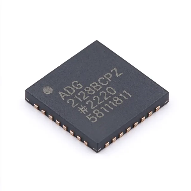
ADG2188BCPZ - 8x8 Analog Crosspoint Switch | Analog Devices
The ADG2188BCPZ is an 8x8 analog crosspoint switch from Analog Devices, designed for routing analog signals in telecommunications, ultrasound, and audio applications. It features 64 bidirectional switch channels arranged in an 8x8 array, with each switch individually addressable via an I2C-compatible interface. The device operates from a single 3.3V or 5V supply and is available in a 32-lead LFCSP-VQ (5x5 mm) package. An analog crosspoint switch is a matrix of switches that connects any input to any output, enabling flexible signal routing without external wiring. It is a key building block in signal routing systems, allowing multiple signals to be directed to different destinations under software control. The ADG2188 belongs to the family of analog switches and multiplexers, which are essential in applications requiring signal distribution and switching. Key features include low on-resistance, low leakage currents, and high bandwidth, ensuring minimal signal distortion. The I2C interface supports standard, full, and fast modes, allowing easy integration with microcontrollers. The device also includes an address pin for multiple device configuration on the same bus, and a reset pin for initialization. Technically, the ADG2188 uses CMOS technology to achieve low power consumption and high switching speed. The switch array is bidirectional, meaning rows and columns can be configured as inputs or outputs, providing flexibility in signal routing. The device also features break-before-make switching to prevent momentary short circuits during channel changes. Typical applications include telecommunications switching, ultrasound imaging, audio routing, and automatic test equipment. In telecommunications, it can route multiple channels in a central office; in ultrasound, it can switch transducer elements; in audio, it can route signals in mixing consoles. When designing with the ADG2188, ensure proper decoupling of the power supply and careful layout to minimize crosstalk. The I2C address pins should be set correctly to avoid bus conflicts. The device is RoHS compliant and suitable for surface-mount assembly.

ADG2188BCPZ-RL7 - 8x8 Analog Crosspoint Switch | Analog Devices
The ADG2188BCPZ-RL7 is an I2C CMOS 8x8 unbuffered analog switch array from Analog Devices, designed for routing analog signals in telecommunications, ultrasound, and audio applications. It provides 64 bidirectional switch channels arranged in eight columns by eight rows, with each switch individually addressable via a standard I2C-compatible interface. The device operates from dual or single supplies, supporting a wide analog signal range, and is housed in a compact 32-lead LFCSP-VQ (5x5 mm) package. An analog crosspoint switch is a type of analog switch array that allows any input to be connected to any output, enabling flexible signal routing without mechanical relays. It is a key building block in signal routing and switching systems, sitting between discrete analog switches and full digital crosspoint ICs in the signal chain hierarchy. The ADG2188's 8x8 matrix provides a balance of channel count and package size, making it suitable for dense PCB designs. Key features include a low on-resistance of [DATA_NEEDED: on-resistance] ohms, low leakage currents, and a wide operating voltage range. The I2C interface supports standard and full-speed modes, allowing easy integration with microcontrollers. The device also features a reset pin and address pins for multiple device configuration on the same bus. Its bidirectional architecture simplifies PCB layout by allowing rows and columns to be configured as inputs or outputs. Technically, the ADG2188 uses CMOS technology to achieve low power consumption and high signal integrity. The unbuffered architecture preserves signal fidelity, making it ideal for precision analog applications. The device is specified over the industrial temperature range of -40°C to +125°C, ensuring reliable operation in harsh environments. Typical applications include telecommunications switching, ultrasound imaging systems, audio routing, and automated test equipment. In ultrasound, the ADG2188 routes transducer signals to processing channels, while in audio, it enables flexible mixing and routing. Its low distortion and high bandwidth make it suitable for high-frequency signals. When designing with the ADG2188, ensure proper decoupling on the supply pins and consider the on-resistance flatness for precision applications. The I2C address pins allow up to [DATA_NEEDED: number of addressable devices] devices on a single bus, enabling large switch matrices.

ADV202BBCZ - JPEG2000 Video Codec | Analog Devices
The ADV202BBCZ is a single-chip JPEG2000 video codec from Analog Devices, designed for real-time compression and decompression of standard-definition video streams. It supports 16-bit parallel input/output and operates at a maximum clock frequency of 150 MHz, enabling high-throughput processing for broadcast and professional video applications. The device is housed in a 144-ball CSPBGA package (13x13 mm) and operates from a 1.8V core supply with 3.3V I/O, making it suitable for power-sensitive embedded systems. A video codec is a hardware or software component that encodes (compresses) and decodes (decompresses) digital video. The ADV202 implements the JPEG2000 standard (ISO/IEC 15444-1), which uses wavelet-based compression to achieve high image quality at low bit rates. As a dedicated codec IC, it offloads computationally intensive processing from host processors, enabling real-time video streaming in applications such as broadcast infrastructure, medical imaging, and surveillance systems. Key features include support for both lossy and lossless compression, programmable compression ratios, and a flexible host interface that supports both parallel and serial (SPI) modes. The device also includes an internal DMA controller for efficient data transfer, and its low power consumption (typically 1.5W) makes it ideal for portable and embedded designs. The ADV202BBCZ is part of the ADV202 family, which includes speed grades of 115 MHz and 150 MHz, with the BBCZ suffix indicating the 150 MHz version in a CSPBGA package. Technically, the ADV202 integrates a wavelet transform engine, an entropy coder, and a rate control unit on a single die. It accepts raw video data in various formats, including YCbCr 4:2:2 and 4:4:4, and outputs compressed JPEG2000 streams. The device supports resolutions up to 720x576 (D1) at 30 fps, making it suitable for standard-definition video processing. Its architecture allows for low-latency encoding, which is critical for real-time applications. Typical applications include video surveillance systems, medical imaging devices, broadcast video servers, and digital cinema. The ADV202BBCZ is also used in military and aerospace systems for secure video transmission. Its robust design and long-term availability make it a preferred choice for industrial and professional video equipment. When designing with the ADV202BBCZ, ensure proper decoupling of the 1.8V core supply and 3.3V I/O supply, and follow the recommended PCB layout guidelines in the datasheet to minimize noise and ensure signal integrity. The device requires an external clock source and configuration via its host interface before video processing can begin.
ADV202BBCZ-RL - JPEG2000 Video Codec | Analog Devices
The ADV202BBCZ-RL is a single-chip JPEG2000 video codec from Analog Devices, designed for real-time compression and decompression of video streams. It supports a 16-bit interface and operates at a clock speed of up to 150 MHz, enabling high-throughput processing for broadcast and professional video applications. The device is housed in a 144-ball CSPBGA package (13x13 mm), offering a compact solution for space-constrained designs. A video codec is an integrated circuit that encodes and decodes digital video signals, converting raw video data into compressed formats for efficient storage and transmission. The ADV202BBCZ-RL specifically implements the JPEG2000 standard, which uses wavelet-based compression to deliver superior image quality at high compression ratios. This codec sits within the broader category of multimedia processors, bridging raw video capture and digital transmission systems. Key features of the ADV202BBCZ-RL include support for JPEG2000 Part 1, a 16-bit host interface, and a maximum clock frequency of 150 MHz. The device offers low power consumption, making it suitable for portable and embedded systems. Its 144-ball CSPBGA package provides excellent thermal performance and a small footprint, ideal for dense PCB layouts. Technically, the ADV202BBCZ-RL integrates a wavelet transform engine, entropy coder, and rate control logic on a single die. This architecture enables real-time encoding and decoding of high-definition video without external processing. The device supports multiple resolution levels and quality layers, allowing flexible bitrate control for various applications. Typical applications include broadcast video servers, medical imaging systems, surveillance DVRs, and digital cinema equipment. The codec's high throughput and low latency make it well-suited for real-time video processing where image fidelity is critical. When designing with the ADV202BBCZ-RL, ensure proper decoupling of the power supply pins and follow the recommended layout guidelines in the datasheet to minimize signal integrity issues. The device requires a clean clock source and careful attention to thermal management due to its high-speed operation.

ADV3002BSTZ - 4:1 HDMI/DVI Switch with EDID | Analog Devices
The Analog Devices ADV3002BSTZ is a 4:1 HDMI/DVI link switch with equalized transition-minimized differential signaling inputs, bidirectional DDC and CEC buffering, EDID replication, and an 80-lead LQFP surface-mount package measuring 14 mm by 14 mm. It is designed to route four digital-video inputs to one output while supporting systems that encounter long cable runs. An HDMI/DVI link switch is a signal-routing interface IC within the broader video-processing and interface-controller hierarchy. The ADV3002 combines the active video-link path with the auxiliary communication paths required by HDMI equipment. Equalization on the TMDS inputs helps recover signals traveling through longer cables, while DDC and CEC buffering isolates auxiliary traffic from the main video connection. The primary feature set includes four inputs, one output, integrated input equalization, bidirectional DDC-bus buffering, CEC-line buffering with integrated pull-up resistors, and EDID replication. The device supports HDMI 1.4a according to the product listing, while the family documentation also references HDMI 1.3a. Input pins provide ±8 kV ESD protection, adding a useful protection layer for externally connected equipment. ADV3002BSTZ is controlled through an I2C-compatible serial interface. In a typical receiver, source detection, switch control, EDID handling, and auxiliary-line communication are combined into one device instead of requiring separate discrete switches and buffers. The equalized inputs make the switch applicable where multiple source cables vary in length or where source-to-display distance makes clean signal recovery important. Typical applications include television and display input selection, HDMI extenders and distribution equipment, professional video systems, set-top boxes, projectors, and multi-source presentation equipment. EDID replication supports source-side display identification, while DDC and CEC buffering allows connected equipment to continue exchanging control data through the selected link. PCB implementation requires care around high-speed TMDS and auxiliary signals. The manufacturer datasheet recommends short CEC and DDC traces, direct connections from bypass-capacitor landing pads to supply pins, and clearance beneath auxiliary traces when the adjacent layer can act as a reference plane. These layout practices reduce parasitic inductance and unwanted coupling. This product page combines the manufacturer product information, technical datasheet guidance, drop-in replacement assessment, application use cases, and implementation notes. It highlights why the ADV3002BSTZ fits multi-input HDMI/DVI equipment while keeping sourcing, lifecycle, packaging, and design decisions in one engineering-focused reference.

ADV3203ASWZ - 300 MHz 32x16 Buffered Crosspoint | Analog Devices
Analog Devices ADV3203ASWZ is a 300 MHz, 32 x 16 buffered analog crosspoint switch with a 176-lead LQFP exposed-pad package, a gain of +2, and a selectable sync-tip clamp input. The integrated routing matrix provides nonblocking signal paths for high-density analog video applications, while a 2:1 on-screen display insertion multiplexer supports OSD integration at each output. The device accepts single +5 V, dual ±2.5 V, or dual ±3.3 V supply arrangements when operating with the specified gain. An analog crosspoint switch is a matrix of buffered inputs and outputs that can route multiple signals through independently selected connections. In the product hierarchy, the ADV3203ASWZ is an analog crosspoint switch, a specialized interface IC, and ultimately a semiconductor designed for high-density routing. Unlike mechanical or passive matrix devices, it combines programmable routing, active buffering, signal isolation, and OSD insertion in one integrated circuit. Key performance features include 300 MHz operating bandwidth, 0.1 dB gain flatness through 60 MHz, -48 dB crosstalk at 5 MHz, and -80 dB isolation at 5 MHz. These characteristics support routing of wideband composite or component video signals where amplitude consistency and rejection of unwanted paths are important. The buffer also provides high-impedance output disable, allowing multiple devices to be connected for expanded routing capacity with minimal output-loading interaction. The internal architecture provides 32 x 16 nonblocking switching, a +2 video gain stage, and a selectable sync-tip clamp suitable for AC-coupled signal paths. Serial programming controls the switch array, reducing the number of control connections required by a large routing system. A separate 2:1 OSD insertion mux is available per output, allowing graphics or overlay information to be combined with the primary routed video path. Typical applications include professional video routers, broadcast production equipment, audiovisual distribution systems, presentation equipment, surveillance-video switching systems, and industrial monitoring panels. The 176-lead LQFP package with exposed pad supports high-density PCB routing while requiring careful thermal design because it contains many active buffered switching paths. Layout should preserve short analog traces, provide clean supply distribution, and place decoupling close to the supply pins. Because the exposed pad is an electrical and thermal connection, its PCB implementation must follow the package guidance. Signal-integrity checks should include return loss, gain flatness, crosstalk, isolation, and output-disable behavior across the intended video bandwidth. This page combines verified manufacturer information, distributor availability and pricing, same-family alternatives, and application-oriented design guidance. It distinguishes directly related family members from broad cross-reference search tools and identifies unavailable pin-level or qualification data rather than estimating it.

ADV3205JSTZ - 60 MHz Buffered Analog Crosspoint | Analog Devices
Analog Devices ADV3205JSTZ is a fully buffered analog crosspoint switch matrix designed for video signal routing. The device provides a 16 × 16 switch arrangement, a specified signal bandwidth of 60 MHz, and a gain of +2 dB. It operates from ±5 V according to the manufacturer description, making it suitable for systems that need buffered analog routing with controlled impedance and improved signal isolation. The ADV3205JSTZ is identified in distributor data as a one-channel video switch IC in a 100-lead LQFP package measuring 14 mm × 14 mm. An analog crosspoint switch is a semiconductor routing matrix that connects one source signal to one destination while buffering the selected path. Unlike an unbuffered passive matrix, the ADV3205 provides active buffering, which can reduce loading effects and support controlled signal transfer between source and destination stages. In a broader equipment hierarchy, it belongs to the analog switch and signal-routing category, within interface and video-routing applications. Its buffered architecture is particularly relevant when the routed signal must remain useful across multiple video-processing stages. The principal verified performance characteristics are 60 MHz signal bandwidth, +2 dB gain, a 16 × 16 matrix, operation from ±5 V, and channel switching time below 60 ns with 0.1% settling. The switching-time figure indicates how quickly the device changes routing state, while the settling specification describes the time required for the output to reach the specified accuracy. The low settling behavior can be valuable in measurement, broadcast, test-equipment, and video-processing systems where a new source must be selected quickly. The ADV3205 also includes ground and power pins around the inputs and outputs to provide shielding between signal paths. This arrangement is intended to improve isolation for demanding analog-routing applications and can reduce coupling between adjacent channels when the PCB layout and grounding system are implemented carefully. The manufacturer identifies the device as recommended for new designs and markets it for video applications, so it is positioned as an active analog-routing solution rather than a simple discrete switch. Typical uses include professional video routing, camera and monitor signal distribution, laboratory test systems, broadcast equipment, and industrial video control. In these systems, the matrix can route one of multiple source signals to a processing chain or measurement instrument. The active buffering helps maintain signal integrity when routing is combined with downstream amplifiers, converters, or acquisition circuits. Because the verified material does not provide the complete electrical table, exact input impedance, output impedance, channel resistance, power consumption, temperature range, and detailed pin functions cannot be independently confirmed from the supplied sources. Designers should place supply decoupling close to the analog IC and preserve the manufacturer’s recommended grounding and shielding topology around the input and output groups. The 14 mm × 14 mm LQFP package also requires adequate PCB escape routing and thermal consideration for high-frequency signal integrity. The verified distributor pages provide the product identity, package information, headline bandwidth, gain, supply arrangement, and switching behavior; final production design should therefore be validated against the complete Analog Devices datasheet, including absolute maximum ratings, recommended operating conditions, and the complete pinout. This page consolidates the supplied manufacturer and distributor information, practical routing considerations, application guidance, and verified-source links. It distinguishes documented headline specifications from fields that still require confirmation from the full datasheet rather than inferring values that were not provided in the verified data.

ADV3229ACPZ - 750 MHz 8x8 Crosspoint Switch | Analog Devices
Analog Devices ADV3229ACPZ is a high-speed, nonblocking 8 x 8 analog crosspoint switch with a 750 MHz bandwidth, +2 gain output amplifiers, and a 72-lead LFCSP-VQ package measuring 10 x 10 mm. It supports buffered inputs, programmable high-impedance outputs, and drives of 150 ohm loads while operating from positive and negative 5 V supplies. An analog crosspoint switch is a multi-input, multi-output routing matrix that connects any selected input channel to any selected output channel without requiring the inactive channels to terminate. Within the semiconductor hierarchy, the ADV3229ACPZ is an analog switch IC, an interface IC, and a signal-routing device for high-frequency video, telecommunications, broadcast, and test equipment. Its nonblocking architecture allows supported channels to remain active while other crosspoint routes change. Key features include an 8 x 8 switch array, eight buffered inputs, eight programmable high-impedance outputs, and eight output amplifiers configured for a gain of +2. The device is specified for 150 ohm loads and low power consumption of 0.5 W. According to the Analog Devices ADV3228/ADV3229 data sheet, its large-signal bandwidth is 750 MHz and its slew rate is 2500 V/us. Technically, the ADV3229 integrates routing switches, input buffers, output amplifiers, and output-disconnect functions into one high-speed analog matrix. The +2 output gain differentiates it from the otherwise closely related ADV3228, which uses +1 gain. The data sheet also identifies the ADV3229 as pinout- and functionally equivalent to the AD8108 and AD8109, making those legacy devices important references when evaluating board compatibility. Typical uses include professional video routing, broadcast video distribution, telecommunications test systems, high-definition signal routing, and instrumentation requiring repeatable high-bandwidth channel selection. The buffered inputs help isolate upstream sources, while the programmable output high-impedance states allow unused outputs to be isolated from driven channels. Designers should verify control-logic levels, exposed-pad grounding, bypass-capacitor placement, and signal-integrity performance on the target board. The 10 x 10 mm land pattern and high-speed analog routing require short connections, a continuous ground reference, and careful control of supply-return paths. Because the ADV3229 uses dual-rail supplies, both positive and negative rails must be present with appropriate decoupling. This page consolidates manufacturer features, distributor pricing, verified source links, same-family drop-in alternatives, and practical selection guidance. It also distinguishes confirmed pin-compatible options from legacy functionally equivalent devices so engineers can verify every footprint, gain, and control requirement before redesigning an existing PCB.
ADV7171KS - 10-Bit PAL/NTSC Video Encoder | Analog Devices
The Analog Devices ADV7171KS is an integrated digital PAL/NTSC video encoder with a 10-bit DAC and advanced power management, packaged in a 44-lead MQFP. According to the manufacturer product page, it converts Digital CCIR-601 4:2:2 8-bit or 16-bit component video data into a standard analog baseband television signal compatible with worldwide standards. The encoder is designed for DVD playback systems, portable video equipment, digital still cameras, laptop PCs, video games, and PC video or multimedia systems. A digital video encoder is an interface and signal-conversion IC that accepts parallel digital video, applies encoding and color-processing functions, and generates composite or component analog video suitable for display equipment. Its role in the signal chain is between a digital video source and an analog display or broadcast interface. The ADV7171 family supports serial control through a 2-wire I2C-compatible interface and uses two slave addresses, allowing configuration of operating modes and encoder functions from a host controller. The key verified feature set includes Digital CCIR-601 4:2:2 input support in either 8-bit or 16-bit formats, a 10-bit DAC, PAL and NTSC encoding capability, and advanced power management. The Analog Devices family description identifies the device as an integrated digital video encoder rather than a general-purpose processor. Its 44-lead MQFP package provides a defined gull-wing footprint for conventional surface-mount PCB assembly and is available in industrial-temperature component listings. The ADV7171KS is appropriate when a design must preserve a digital video source while producing standard analog baseband output. The serial control interface simplifies integration with source-specific firmware, while the dedicated video encoder reduces the need for external DAC and encoding circuitry. Engineers should still verify clocking, sync polarity, pixel clock relationships, output loading, power sequencing, and analog video quality against the complete manufacturer datasheet before releasing a production layout. Typical applications include DVD playback systems, portable video equipment, digital still cameras, laptop computers, video games, and PC video or multimedia products. In these systems, the encoder can convert decoded digital video into PAL or NTSC-compatible analog signals for downstream display or capture equipment. The dedicated encoder also supports integration into compact consumer products where board area and external component count are important. A key design consideration is that analog baseband video requires careful PCB layout and signal-integrity control. Keep the encoder clock and digital-video traces away from sensitive output paths, provide clean power and ground connections, and follow the manufacturer’s recommended decoupling and output-network details. Because the supplied web data does not expose the complete electrical timing table, pin names, or exact operating limits, those values should not be inferred from generic video-encoder specifications. This page consolidates verified manufacturer and distributor information, including the ADV7171KS application context, package identity, family capabilities, and replacement-search results. It is intended to support component selection and engineering research while clearly separating verified facts from parameters that still require confirmation in the complete ADV7170/ADV7171 datasheet.

ADV7171KSU 10-Bit PAL/NTSC Video Encoder | Analog Devices
Analog Devices ADV7171KSU is an integrated 10-bit digital video encoder that converts ITU-R BT.601/656 YCrCb 4:2:2 component data into standard PAL or NTSC analog baseband video. The device provides four video DAC outputs and is supplied in a surface-mount 44-pin TQFP package measuring 10 mm by 10 mm. Its primary function is to bridge a digital video source and legacy analog composite, S-Video, or component outputs. A video encoder is a signal-conversion semiconductor that accepts digital pixel data and generates an analog waveform accepted by PAL or NTSC display equipment. Within the product hierarchy, the ADV7171 is an interface IC and video encoder rather than a processor or display driver. The corresponding digital-video-to-analog-video conversion stage sits between a video source, such as a DVD controller or multimedia processor, and an analog video connector or display. According to the Analog Devices ADV7171 product page, the encoder supports 8-bit or 16-bit CCIR-601 4:2:2 component video input. Its four 10-bit DACs support PAL and NTSC generation, while its digital video input follows the BT.601/656 format identified in the provided product information. This integration reduces the need for external video DACs when a design requires both S-Video and composite or additional analog video outputs. The ADV7170 and ADV7171 family is positioned for high-performance DVD playback, portable video equipment, digital still cameras, laptop computers, video games, and PC video or multimedia systems. The supplied search data does not provide verified clock frequency, power-supply range, output voltage resolution, operating temperature, timing limits, or package dimensions beyond the 10 mm by 10 mm TQFP description, so those values are not inferred here. The main engineering concern is interface compatibility rather than power conversion. The source must supply correctly timed BT.601/656 YCrCb data, the PCB must route high-speed digital video signals without excessive distortion, and analog outputs must be terminated according to the selected PAL or NTSC standard. The exact clocking, synchronization, control-register, and DAC configuration procedure must be taken from the manufacturer data sheet rather than inferred from the order code. For procurement, ADV7171KSUZ and ADV7171KSUZ-REEL appear in the supplied cross-reference results as the same 44-pin device with compatible terminals and characteristics, but the KSUZ order codes may represent ordering or reel-packaging conventions rather than five distinct functional alternatives. This page therefore distinguishes verified function-level choices from packaging suffixes and does not present reel-code variants as separate engineering options. This page consolidates the supplied manufacturer description, distributor package information, cross-reference findings, application guidance, and unresolved-data warnings. It is intended to support engineering selection and sourcing while directing readers to the manufacturer data sheet for authoritative electrical limits, pin functions, register definitions, and timing specifications.
ADV7171KSU-REEL 10-Bit PAL/NTSC Video Encoder | Analog Devices (Tape & Reel)
Analog Devices ADV7171KSU-REEL is an integrated 10-bit digital video encoder that converts ITU-R BT.601/656 YCrCb 4:2:2 component data into standard PAL or NTSC analog baseband video. The device provides four video DAC outputs and is supplied in a surface-mount 44-pin TQFP package measuring 10 mm by 10 mm. Its primary function is to bridge a digital video source and legacy analog composite, S-Video, or component outputs. A video encoder is a signal-conversion semiconductor that accepts digital pixel data and generates an analog waveform accepted by PAL or NTSC display equipment. Within the product hierarchy, the ADV7171 is an interface IC and video encoder rather than a processor or display driver. The corresponding digital-video-to-analog-video conversion stage sits between a video source, such as a DVD controller or multimedia processor, and an analog video connector or display. According to the Analog Devices ADV7171 product page, the encoder supports 8-bit or 16-bit CCIR-601 4:2:2 component video input. Its four 10-bit DACs support PAL and NTSC generation, while its digital video input follows the BT.601/656 format identified in the provided product information. This integration reduces the need for external video DACs when a design requires both S-Video and composite or additional analog video outputs. The ADV7170 and ADV7171 family is positioned for high-performance DVD playback, portable video equipment, digital still cameras, laptop computers, video games, and PC video or multimedia systems. The supplied search data does not provide verified clock frequency, power-supply range, output voltage resolution, operating temperature, timing limits, or package dimensions beyond the 10 mm by 10 mm TQFP description, so those values are not inferred here. The main engineering concern is interface compatibility rather than power conversion. The source must supply correctly timed BT.601/656 YCrCb data, the PCB must route high-speed digital video signals without excessive distortion, and analog outputs must be terminated according to the selected PAL or NTSC standard. The exact clocking, synchronization, control-register, and DAC configuration procedure must be taken from the manufacturer data sheet rather than inferred from the order code. For procurement, ADV7171KSU-REELZ and ADV7171KSU-REELZ-REEL appear in the supplied cross-reference results as the same 44-pin device with compatible terminals and characteristics, but the KSUZ order codes may represent ordering or reel-packaging conventions rather than five distinct functional alternatives. This page therefore distinguishes verified function-level choices from packaging suffixes and does not present reel-code variants as separate engineering options. This page consolidates the supplied manufacturer description, distributor package information, cross-reference findings, application guidance, and unresolved-data warnings. It is intended to support engineering selection and sourcing while directing readers to the manufacturer data sheet for authoritative electrical limits, pin functions, register definitions, and timing specifications.
ADV7171KSZ - PAL/NTSC Video Encoder | Analog Devices
Analog Devices ADV7171KSZ is an integrated digital PAL/NTSC video encoder with a 10-bit SSAF architecture and advanced power management, supplied in a 44-MQFP package measuring 10 x 10 mm. The device accepts digital CCIR-601 4:2:2 component video in either 8-bit or 16-bit form and converts it into a standard analog baseband television signal compatible with worldwide PAL and NTSC systems. An integrated video encoder is a signal-processing IC that bridges a digital video pipeline and an analog composite or component output. In the product hierarchy, the ADV7171 belongs to video codecs and converters, within interface ICs, rather than acting as a general-purpose processor or display driver. Its principal purpose is to preserve useful picture information while translating digital video data into the modulation and level characteristics required by legacy analog television equipment. Three headline characteristics define the ADV7171KSZ: 10-bit SSAF video conversion, digital PAL/NTSC encoding, and operation from a 4.75 V to 5.25 V analog supply. The 4.75 V to 5.25 V supply range supports conventional 5 V equipment designs, while the 44-MQFP package provides 44 externally accessible connections for digital data, control, clocking, power, and analog output functions. The manufacturer describes the family as suitable for high-performance DVD playback, portable video equipment, digital still cameras, laptop PCs, video games, and PC multimedia systems. Advanced power management is a central feature of the device family. According to the Analog Devices ADV7170/ADV7171 datasheet, the encoder can use its SCRESET/RTC pin together with Mode Register 2 bits MR22 and MR21 to lock to an external video source. The real-time control mode automatically alters the subcarrier frequency to compensate for line-length variation. These functions allow an encoder to remain synchronized with an external source when its timing differs from the nominal internal reference. Typical implementations place the ADV7171KSZ between a digital video source and an analog video connector or downstream display. A DVD player can feed decoded video into the encoder for compatibility with a PAL or NTSC television. Portable equipment can use the same conversion function when an analog video output is required, while PC video and multimedia designs use it as a bridge from digital graphics or decoded video to an external analog display. The primary design consideration is that the ADV7171KSZ is a legacy-standard bridge rather than a modern HDMI or display-port transmitter. Designers must confirm signal timing, input word width, output standard, synchronization behavior, and analog output integration before layout release. The Analog Devices product page marks the ADV7171 as not recommended for new designs, so new products should evaluate current encoder options unless legacy equipment requires exact compatibility. This page combines manufacturer capabilities, distributor availability, package information, lifecycle status, and verified replacement candidates. It also identifies where pin-level and pricing information remains unavailable, helping engineers distinguish confirmed device data from details that must be checked against the official datasheet and authorized distribution channels.
ADV7171KSZ-REEL - PAL/NTSC Video Encoder | Analog Devices (Tape & Reel)
Analog Devices ADV7171KSZ-REEL is an integrated digital PAL/NTSC video encoder with a 10-bit SSAF architecture and advanced power management, supplied in a 44-MQFP package measuring 10 x 10 mm. The device accepts digital CCIR-601 4:2:2 component video in either 8-bit or 16-bit form and converts it into a standard analog baseband television signal compatible with worldwide PAL and NTSC systems. An integrated video encoder is a signal-processing IC that bridges a digital video pipeline and an analog composite or component output. In the product hierarchy, the ADV7171 belongs to video codecs and converters, within interface ICs, rather than acting as a general-purpose processor or display driver. Its principal purpose is to preserve useful picture information while translating digital video data into the modulation and level characteristics required by legacy analog television equipment. Three headline characteristics define the ADV7171KSZ-REEL: 10-bit SSAF video conversion, digital PAL/NTSC encoding, and operation from a 4.75 V to 5.25 V analog supply. The 4.75 V to 5.25 V supply range supports conventional 5 V equipment designs, while the 44-MQFP package provides 44 externally accessible connections for digital data, control, clocking, power, and analog output functions. The manufacturer describes the family as suitable for high-performance DVD playback, portable video equipment, digital still cameras, laptop PCs, video games, and PC multimedia systems. Advanced power management is a central feature of the device family. According to the Analog Devices ADV7170/ADV7171 datasheet, the encoder can use its SCRESET/RTC pin together with Mode Register 2 bits MR22 and MR21 to lock to an external video source. The real-time control mode automatically alters the subcarrier frequency to compensate for line-length variation. These functions allow an encoder to remain synchronized with an external source when its timing differs from the nominal internal reference. Typical implementations place the ADV7171KSZ-REEL between a digital video source and an analog video connector or downstream display. A DVD player can feed decoded video into the encoder for compatibility with a PAL or NTSC television. Portable equipment can use the same conversion function when an analog video output is required, while PC video and multimedia designs use it as a bridge from digital graphics or decoded video to an external analog display. The primary design consideration is that the ADV7171KSZ-REEL is a legacy-standard bridge rather than a modern HDMI or display-port transmitter. Designers must confirm signal timing, input word width, output standard, synchronization behavior, and analog output integration before layout release. The Analog Devices product page marks the ADV7171 as not recommended for new designs, so new products should evaluate current encoder options unless legacy equipment requires exact compatibility. This page combines manufacturer capabilities, distributor availability, package information, lifecycle status, and verified replacement candidates. It also identifies where pin-level and pricing information remains unavailable, helping engineers distinguish confirmed device data from details that must be checked against the official datasheet and authorized distribution channels.

ADV7173KST - 10-Bit Six-DAC Video Encoder | Analog Devices
The Analog Devices ADV7173KST is a digital PAL/NTSC video encoder with six 10-bit DACs, color control, and enhanced power management, housed in a 48-lead LQFP package measuring 7 mm x 7 mm. It converts digital CCIR-601 4:2:2 8-bit component video data into standard analog baseband television signals compatible with worldwide PAL and NTSC systems. A manufacturer list price of $10.79 was shown as of 2026-10-28, while one authorized marketplace listing offered the component from $3.9879. A digital video encoder is an interface and signal-conversion integrated circuit. It belongs to the video codec, video interface, interface IC, and broader semiconductor hierarchy. The encoder accepts already digitized component video, generates the required analog color and luminance outputs, and provides the bridge between a digital video-processing pipeline and a conventional PAL or NTSC display or video system. The ADV7173 provides six 10-bit DACs within one integrated encoder. The six-output arrangement supports generation of the component signals required for PAL or NTSC baseband video. Color-control functions allow the encoder to participate in calibrated video paths, while enhanced power management provides device-level control suited to systems where analog video circuitry must coexist with digital processing. The ADV7173 operates with an 8-bit CCIR-601 4:2:2 component-video interface. This representation separates luminance and chrominance information and reduces chrominance resolution relative to the full raster. The encoder converts that digital representation into standard analog baseband television signals, with the resulting format selected for the target television system. Typical uses include PAL and NTSC video encoding, digital video processing equipment, broadcast and professional video interfaces, video test systems, and embedded analog-video output stages. The encoder is especially relevant when a system must retain a conventional analog television output while accepting digital component video from an image processor, frame grabber, scaler, or video controller. Designers should treat the complete ADV7173 data sheet as the controlling reference for supply voltages, timing, DAC configuration, sync generation, control registers, and application schematics. Because the supplied search excerpts identify the 48-lead LQFP package but do not expose the complete numbered pinout, the pin assignment must be verified in the manufacturer data sheet before PCB routing or replacement qualification. This page consolidates the verified manufacturer description, marketplace price observations, package information, comparison targets, and practical qualification considerations. It distinguishes confirmed characteristics from unavailable specifications so engineers can make an evidence-based sourcing or drop-in replacement decision without relying on an inferred pinout.
ADV7173KST-REEL - 10-Bit Six-DAC Video Encoder | Analog Devices (Tape & Reel)
The Analog Devices ADV7173KST-REEL is a digital PAL/NTSC video encoder with six 10-bit DACs, color control, and enhanced power management, housed in a 48-lead LQFP package measuring 7 mm x 7 mm. It converts digital CCIR-601 4:2:2 8-bit component video data into standard analog baseband television signals compatible with worldwide PAL and NTSC systems. A manufacturer list price of $10.79 was shown as of 2026-10-28, while one authorized marketplace listing offered the component from $3.9879. A digital video encoder is an interface and signal-conversion integrated circuit. It belongs to the video codec, video interface, interface IC, and broader semiconductor hierarchy. The encoder accepts already digitized component video, generates the required analog color and luminance outputs, and provides the bridge between a digital video-processing pipeline and a conventional PAL or NTSC display or video system. The ADV7173 provides six 10-bit DACs within one integrated encoder. The six-output arrangement supports generation of the component signals required for PAL or NTSC baseband video. Color-control functions allow the encoder to participate in calibrated video paths, while enhanced power management provides device-level control suited to systems where analog video circuitry must coexist with digital processing. The ADV7173 operates with an 8-bit CCIR-601 4:2:2 component-video interface. This representation separates luminance and chrominance information and reduces chrominance resolution relative to the full raster. The encoder converts that digital representation into standard analog baseband television signals, with the resulting format selected for the target television system. Typical uses include PAL and NTSC video encoding, digital video processing equipment, broadcast and professional video interfaces, video test systems, and embedded analog-video output stages. The encoder is especially relevant when a system must retain a conventional analog television output while accepting digital component video from an image processor, frame grabber, scaler, or video controller. Designers should treat the complete ADV7173 data sheet as the controlling reference for supply voltages, timing, DAC configuration, sync generation, control registers, and application schematics. Because the supplied search excerpts identify the 48-lead LQFP package but do not expose the complete numbered pinout, the pin assignment must be verified in the manufacturer data sheet before PCB routing or replacement qualification. This page consolidates the verified manufacturer description, marketplace price observations, package information, comparison targets, and practical qualification considerations. It distinguishes confirmed characteristics from unavailable specifications so engineers can make an evidence-based sourcing or drop-in replacement decision without relying on an inferred pinout.
ADV7173KSTZ - PAL/NTSC Video Encoder | Analog Devices
The Analog Devices ADV7173KSTZ is a digital PAL/NTSC video encoder IC with six 10-bit DACs, a 3 V to 3.6 V supply range, and a 48-LQFP 7 mm × 7 mm package. It converts digital CCIR-601 4:2:2 8-bit component video into standard analog baseband television signals compatible with worldwide video standards. A video encoder is an interface IC that bridges a digital video-processing system and an analog video connection. It accepts parallel digital component-video data, applies the required encoding and signal conversion, and produces composite video plus selectable S-VHS Y/C, RGB, or YUV outputs. The ADV7173 integrates six DACs so multiple analog outputs can be generated without separate external converter stages. The device supports PAL and NTSC encoding, color-signal control, burst-signal control, and enhanced power management. Its six 10-bit DACs provide the analog output resolution stated for the ADV7172/ADV7173 family, while the digital input path is specified as CCIR-601 4:2:2 8-bit component data. These features make the encoder useful in video test equipment, broadcast processing equipment, industrial imaging systems, and legacy audiovisual installations where digital video must be converted to analog baseband signals. The commercial ADV7173KSTZ ordering code uses a 48-lead LQFP package and is specified for a 0 °C to +70 °C operating range. The 7 mm × 7 mm surface-mount package provides 48 terminals in a gull-wing square format. A single 3 V to 3.6 V supply range supports integration with contemporary 3.3 V digital logic, although each board still requires suitable analog-output drive, bypassing, and signal-routing discipline. When designing around the ADV7173KSTZ, verify the complete pin assignment and timing relationships in the manufacturer datasheet before routing the board. Keep analog outputs away from high-speed digital clocks, provide local supply decoupling at the device, and observe the video timing requirements for the selected PAL or NTSC mode. The encoder’s principal trade-off is that it adds six analog output channels and associated board area instead of using a purely digital video interface. This page consolidates the confirmed encoder specifications, package information, functional use cases, practical design guidance, and verified drop-in alternatives for faster engineering selection and sourcing review.
ADV7173KSTZ-REEL - PAL/NTSC Video Encoder | Analog Devices (Tape & Reel)
The Analog Devices ADV7173KSTZ-REEL is a digital PAL/NTSC video encoder IC with six 10-bit DACs, a 3 V to 3.6 V supply range, and a 48-LQFP 7 mm × 7 mm package. It converts digital CCIR-601 4:2:2 8-bit component video into standard analog baseband television signals compatible with worldwide video standards. A video encoder is an interface IC that bridges a digital video-processing system and an analog video connection. It accepts parallel digital component-video data, applies the required encoding and signal conversion, and produces composite video plus selectable S-VHS Y/C, RGB, or YUV outputs. The ADV7173 integrates six DACs so multiple analog outputs can be generated without separate external converter stages. The device supports PAL and NTSC encoding, color-signal control, burst-signal control, and enhanced power management. Its six 10-bit DACs provide the analog output resolution stated for the ADV7172/ADV7173 family, while the digital input path is specified as CCIR-601 4:2:2 8-bit component data. These features make the encoder useful in video test equipment, broadcast processing equipment, industrial imaging systems, and legacy audiovisual installations where digital video must be converted to analog baseband signals. The commercial ADV7173KSTZ-REEL ordering code uses a 48-lead LQFP package and is specified for a 0 °C to +70 °C operating range. The 7 mm × 7 mm surface-mount package provides 48 terminals in a gull-wing square format. A single 3 V to 3.6 V supply range supports integration with contemporary 3.3 V digital logic, although each board still requires suitable analog-output drive, bypassing, and signal-routing discipline. When designing around the ADV7173KSTZ-REEL, verify the complete pin assignment and timing relationships in the manufacturer datasheet before routing the board. Keep analog outputs away from high-speed digital clocks, provide local supply decoupling at the device, and observe the video timing requirements for the selected PAL or NTSC mode. The encoder’s principal trade-off is that it adds six analog output channels and associated board area instead of using a purely digital video interface. This page consolidates the confirmed encoder specifications, package information, functional use cases, practical design guidance, and verified drop-in alternatives for faster engineering selection and sourcing review.

ADV7174WBCPZ - PAL/NTSC Video Encoder | Analog Devices
The Analog Devices ADV7174WBCPZ is an integrated PAL/NTSC digital video encoder with 10-bit video DACs, 80 dB video SNR, and a 40-lead LFCSP-WQ package measuring 6 mm by 6 mm. It converts digital CCIR-601 4:2:2 8-bit component-video data into a standard analog baseband television signal while requiring a single 27 MHz clock with 2x oversampling. A digital video encoder is a semiconductor interface that transforms digital component-video frames into legacy analog composite or component output. It belongs to the video-processing IC hierarchy alongside decoders, converters, and interface ICs. The ADV7174 combines input timing, noise filtering, color modulation, and video DAC output in one integrated circuit, allowing portable video equipment to produce a television-compatible analog signal from a digital video pipeline. The device supports ITU-R BT.601 and BT.656 YCrCb input and includes SSAF filtering, advanced power-management functions, copy-generation management through CGMS, and wide-screen signaling through WSS. Its 10-bit video DACs support high-quality analog generation, while the 80 dB video SNR provides a measurable signal-quality figure. NTSC M, PAL N2, PAL B/D/G/H/I, PAL M3, and PAL 60 output standards are listed in the manufacturer datasheet. The SSAF filtering architecture reduces unwanted video artifacts associated with digital-to-analog conversion. Direct digital timing architecture, 32-bit internal processing, and the integrated DACs simplify synchronization between a digital video source and an analog television output. The 27 MHz clock requirement provides a common reference for the encoder and its 2x oversampling process, reducing the number of independent clock sources required in the surrounding system. Typical applications include portable digital video products, camera systems, mobile-phone video accessories, video-conversion equipment, and compact consumer electronics that must generate PAL or NTSC baseband video. The integrated format support is especially useful when a product must address multiple television standards without relying on a large collection of external modulation and DAC components. Designers should budget adequate routing space for the analog output, maintain the required power and ground distribution, and validate timing against the source pixel clock. The use of a 6 mm by 6 mm exposed-pad package also requires careful PCB thermal design so heat can transfer away from the device without disturbing sensitive video traces. This page combines the manufacturer’s encoder specifications, package information, application guidance, comparison points, and practical design considerations. It helps engineers evaluate the ADV7174WBCPZ against the closely related ADV7179WBCPZ while preserving the distinction between confirmed device functions and parameters that still require project-specific validation.
ADV7176AKS - 10-Bit 4-DAC PAL/NTSC Video Encoder | Analog Devices
The Analog Devices ADV7176AKS is an integrated 10-bit digital CCIR-601 component-video encoder with four DACs, designed to convert 8-bit or 16-bit 4:2:2 YCrCb data into PAL or NTSC analog baseband video. It is supplied in a 44-pin MQFP package and is intended for professional video equipment, broadcast conversion systems, digital video processors, and other applications requiring deterministic component-video encoding. A video encoder is an interface and signal-conversion device that translates digital component-video data into a legacy analog baseband format accepted by PAL and NTSC equipment. Within the broader product hierarchy, the ADV7176AKS is a video encoder IC, a signal-conversion integrated circuit, and ultimately a semiconductor used within professional video and broadcast equipment. Its CCIR-601 input interface and four analog output DACs consolidate digital-to-analog video conversion into one device. The principal verified feature set includes 10-bit conversion, four DAC outputs, CCIR-601 4:2:2 input, and support for PAL B/D/G/H/I, PAL M, PAL N, and NTSC. Teletext insertion is identified in the verified product listing for the ADV7176AKS. These features make the device relevant where component-video data must be converted into standard analog television signals without relying on a collection of discrete output converters. The 44-pin MQFP package provides 44 electrical connections for digital-video input, clock and control signaling, analog output channels, power, ground, and configuration functions. Exact pin names, voltage ratings, clock requirements, DAC output ranges, and absolute maximum ratings are not included in the supplied source excerpts; engineers should therefore use the Analog Devices ADV7176/ADV7176A manufacturer datasheet for implementation details rather than infer missing values from the family description. Typical uses include PAL/NTSC video recording equipment, professional broadcast and post-production systems, digital-video test equipment, video standards-conversion products, and embedded television interfaces. The part accepts digital data upstream and produces analog baseband outputs downstream, making it suitable for equipment that must bridge modern digital processing with installed analog video infrastructure. The most important design consideration is that this is an obsolete product, so new production designs should account for lifecycle risk, limited supply, and obsolete-product support constraints. Hardware redesign should begin by checking the complete pinout, electrical limits, synchronization requirements, DAC loading, and reference circuitry in the manufacturer datasheet. PCB layout should preserve short analog output paths and controlled digital-clock routing to reduce conversion-quality and timing risks. This page consolidates verified lifecycle information, package details, functional characteristics, source links, and replacement-analysis constraints. It also distinguishes documented functions from unavailable electrical parameters and does not present unverified substitute parts as guaranteed drop-in replacements.