RF Transceivers
بەرهەمەکان (260+)

ADF4116BRU - 550 MHz Integer-N RF PLL | Analog Devices
The Analog Devices ADF4116BRU is a single-band integer-N phase-locked-loop frequency synthesizer with a 550 MHz operating ceiling, a programmable RF prescaler, and a three-wire serial interface, housed in a 16-lead TSSOP package. It is designed to generate stable local-oscillator signals for wireless receivers and transmitters. A frequency synthesizer is a clock-and-timing device that locks an output frequency to a stable reference. The ADF4116 family belongs to the broader RF PLL hierarchy: a phase-frequency detector and precision charge pump compare the divided output with a reference signal, while programmable counters determine the multiplication ratio. This architecture provides programmable frequency generation for RF upconversion, downconversion, modulation, and test equipment. Key features identified in the verified manufacturer data include a 550 MHz maximum operating frequency, a 32/33 dual-modulus prescaler, a 5-bit A counter, a programmable B counter, selectable charge-pump currents, and digital lock detect. The device supports a 5.5 V power supply and a separate VP connection that can extend the tuning-voltage range in suitable 3 V systems. Its serial programming interface simplifies frequency, counter, prescaler, and power-state configuration. Technically, the integer-N architecture uses a dual-modulus prescaler to synthesize many output frequencies from one reference source. The programmable A and B counters divide the prescaled RF signal, while the phase-frequency detector controls the charge-pump current applied to an external loop filter. Correct loop-filter design, reference stability, and RF layout determine practical phase noise and lock performance; the supplied search results do not provide complete phase-noise curves or timing values. Typical uses include wireless receiver and transmitter local oscillators, upconversion and downconversion chains, industrial RF systems, instrumentation, and communication equipment. The 16-TSSOP package is compact and surface-mountable, but exposed-pad thermal details and exact pin names were not provided in the verified data. When replacing this part, verify the complete ADF4116 datasheet pinout, counter limits, reference frequency, prescaler range, supply sequencing, and loop-filter requirements. The verified distributor result also identifies ADF4116BRUZ as the current production variant with identical electrical specifications and pin compatibility, but that claim is not treated as a manufacturer-confirmed drop-in substitute here. This page combines the verified manufacturer and distributor records with engineering guidance, application context, and replacement caveats for engineers evaluating RF PLL layouts.

ADF4150BCPZ-RL7 - 4.4GHz Fractional-N PLL Synthesizer | Analog Devices
The Analog Devices ADF4150BCPZ-RL7 is a fractional-N or integer-N frequency synthesizer IC for RF phase-locked-loop designs, operating up to 4.4 GHz in a 24-lead WFQFN exposed-pad package. The device works with an external voltage-controlled oscillator, loop filter, and reference frequency, providing the core PLL control functions for programmable RF signal generation. It supports fractional-N and integer-N synthesis modes, and the VCO frequency can be divided by 1, 2, 4, 8, or 16 to support RF frequency-generation requirements. According to the Analog Devices ADF4150 product page, the ADF4150 is software compatible with the ADF4350. The ADF4150BCPZ-RL7 designation identifies the Analog Devices frequency-synthesizer family in a 24-lead WFQFN exposed-pad package, with the -RL7 ordering suffix associated with the reel-lead configuration shown by the manufacturer’s product information. This is not a self-oscillating signal source: an external VCO and carefully designed loop filter remain required to complete the RF synthesizer. The device is intended for designers who need programmable RF output, phase control, and flexible divide ratios within an external-VCO PLL architecture. Use the manufacturer datasheet for the complete electrical limits, register map, recommended reference and power-supply circuits, pin descriptions, and timing information before finalizing a design. This page also organizes practical design considerations, replacement questions, and application guidance around the ADF4150BCPZ-RL7 rather than presenting the part as a stand-alone RF oscillator.
ADF4360-3BCP - 1.95GHz Integer-N PLL | Analog Devices
The Analog Devices ADF4360-3BCP is an integer-N frequency synthesizer with an integrated voltage-controlled oscillator, designed for a center frequency of 1750 MHz and operation up to 1.95 GHz. The device is housed in a 24-lead WFQFN exposed-pad package measuring 4 mm by 4 mm. An integer-N PLL frequency synthesizer combines a phase-locked loop, frequency divider, reference input, and VCO to produce a stable programmable RF output. The ADF4360-3 family supports a divide-by-2 operating mode that provides an RF output from 800 MHz to 975 MHz, making the device useful where either a fundamental high-frequency output or a divided lower-frequency output is required. Key features include the 1750 MHz nominal center frequency, operation up to 1.95 GHz, and an integrated VCO that reduces the number of external high-frequency components required in a synthesizer design. The 24-WFQFN exposed-pad package supports compact RF layouts, while its exposed thermal pad provides a path for heat transfer through the PCB. The industrial-grade component is identified as a no-lead, 24-terminal square package. The ADF4360-3 architecture separates synthesis into an integer feedback divider and programmable VCO within one integrated circuit. Its divided output broadens application flexibility without requiring a second synthesizer for the 800 MHz to 975 MHz range. The divide-by-2 function is specifically called out by Analog Devices for the ADF4360-3, making that operating mode the key engineering distinction within the broader ADF4360 family. Typical uses include cellular and baseband RF systems, local oscillators, wireless infrastructure, instrumentation, and frequency-generation modules. A designer can select the output frequency through the synthesizer programming interface and use the reference and feedback paths to establish phase lock. The integrated VCO is particularly useful when board area, component count, and repeatable RF performance are more important than the flexibility of a discrete VCO implementation. PCB implementation requires careful treatment of the reference, feedback, supply, and RF output paths. Keep the exposed pad connected to a low-impedance ground plane and follow the manufacturer's pin-description table and reference-layout guidance when assigning tracks. Validate loop-filter component values, reference-divider settings, and output power for the intended channel plan before releasing a production layout. This product page consolidates the ADF4360-3 frequency ranges, package details, application guidance, comparison information, and sourcing workflow into one engineering-focused reference. It also distinguishes exact drop-in alternatives from related family members whose tuning ranges or MPN suffixes serve different design requirements.
ADF4360-3BCPRL - 1.75GHz Integer-N VCO | Analog Devices
The Analog Devices ADF4360-3BCPRL is a fully integrated integer-N frequency synthesizer with an on-chip voltage controlled oscillator designed for a center frequency of 1750 MHz. The device includes a divide-by-2 output option that produces an RF output between 800 MHz and 975 MHz, and is supplied in a 24-lead WFQFN exposed-pad surface-mount package. Its integrated synthesizer architecture combines a programmable integer-N divider, phase detector, charge pump, VCO, and RF output stages in one device. An integer-N synthesizer is a clock and RF signal-generation component that generates an output frequency through feedback locking to a reference frequency. The ADF4360-3 family is intended for wireless communication, test equipment, instrumentation, and other systems requiring a programmable RF carrier with controlled phase and frequency. The divide-by-2 feature provides flexibility for systems operating below the main VCO frequency while retaining a shared synthesizer architecture. The principal design features include the 1750 MHz VCO center-frequency designation, an RF output range of 800 MHz to 975 MHz in divide-by-2 mode, integrated integer-N operation, and a 3 V to 3.6 V supply range. The device is intended for surface-mount assembly and is identified in product listings as a 24-terminal WFQFN package with an exposed pad. Its integrated VCO reduces the number of external high-frequency components required for a complete local oscillator implementation. In practice, the ADF4360-3BCPRL is used where a compact programmable RF source is more useful than a fixed crystal oscillator. The on-chip VCO, feedback divider, and phase-locked-loop functions make the device appropriate for RF signal generation, frequency hopping, modulation, communications test equipment, and industrial RF systems. The exact tuning range, reference-frequency limits, output-power characteristics, noise performance, and register map should be confirmed against the manufacturer datasheet before final circuit design. The exposed-pad package requires careful PCB layout to remove heat from the die and maintain reliable electrical performance at the intended operating temperature. Place power and ground connections according to the recommended land pattern, connect the exposed pad to the appropriate ground plane, and keep sensitive reference and control traces away from noisy RF output paths. The 3 V to 3.6 V supply range also requires stable decoupling close to the device. This product page combines the manufacturer product information, package identification, application guidance, and practical design considerations. It is intended to help engineers determine whether the ADF4360-3BCPRL matches a required RF frequency range, package footprint, supply requirement, and integration level before requesting a quotation or beginning a hardware design.
ADF4360-5BCP - 1.3 GHz Integer-N Synthesizer | Analog Devices
Analog Devices ADF4360-5BCP is a fully integrated integer-N frequency synthesizer and voltage-controlled oscillator with a 1300 MHz design center frequency, an RF output range extending to 1.4 GHz, and a divide-by-2 output covering 600 MHz to 700 MHz. The device is housed in a 24-lead WFQFN exposed-pad package and uses a three-wire register interface. An integer-N frequency synthesizer combines a phase-locked loop, frequency divider, and voltage-controlled oscillator to generate a stable RF output. The VCO supplies the high-frequency reference within the tuning system, while the synthesizer locks that signal to a stable reference. The ADF4360-5 integrates these functions to support RF clock generation, local oscillator creation, and frequency conversion within communications and signal-processing equipment. The principal feature of the ADF4360-5 is its integrated RF VCO for the 1300 MHz-centered design range. Its divide-by-2 operating mode provides a second output range from 600 MHz to 700 MHz. This combination allows one synthesizer to support RF signals in both the 1.15 GHz to 1.4 GHz class and the lower 600 MHz to 700 MHz class, subject to the register settings and external support circuitry selected for the design. All on-chip registers are accessed through a simple three-wire interface. This architecture reduces the number of control connections required when the synthesizer is paired with a microcontroller, embedded processor, or dedicated serial controller. The 24-WFQFN exposed-pad package provides a compact surface-mount implementation, while the exposed pad provides the thermal connection needed when operating across the device's frequency range. Typical uses include local oscillator generation in RF communications equipment, clocking for mixers and converters, test-and-measurement signal sources, and frequency-generation stages in industrial or wireless systems. In each case, the reference frequency, loop filter, output power, and register configuration determine whether the synthesized output meets the application's phase-noise, tuning, and output-level requirements. PCB implementation should preserve the layout and grounding practices associated with the exposed-pad package. The three-wire control signals require suitable trace routing, and the RF output path should use controlled impedance and short return paths. The power and ground connections must provide low-impedance distribution because resistance and inductance in those paths can affect oscillator behavior and phase noise. This product record combines the manufacturer's functional description with distributor package and ordering information. It also organizes practical sourcing questions, pin-compatible alternatives, application guidance, and the design considerations that matter when integrating a high-frequency integer-N synthesizer.
ADF4360-7BCPZ - 1.8 GHz Integer-N Synthesizer | Analog Devices
The Analog Devices ADF4360-7BCPZ is an integrated integer-N frequency synthesizer and voltage-controlled oscillator that delivers an output frequency range of 350 MHz to 1800 MHz in a 24-lead LFCSP package with an exposed pad. It combines a programmable dual-modulus prescaler, phase detector, reference divider, charge-pump circuitry, and VCO core in one device. A divide-by-2 output mode expands the usable RF output range to 175 MHz to 900 MHz. The synthesizer operates from a 3.0 V to 3.6 V supply and is compatible with 1.8 V logic levels, making it practical for modern RF and baseband control systems. An integer-N synthesizer is a PLL-based frequency generator that produces an output by multiplying a stable reference frequency by an integer ratio. Its phase noise, reference multiplication, spur performance, and tuning range are central design considerations. The ADF4360-7 uses external inductors to establish the VCO center frequency, allowing the same silicon to cover different frequency bands through component selection and firmware programming. This architecture places the synthesizer within the broader category of clock and frequency-generation ICs used by RF transceivers, test equipment, and communication infrastructure. Key features include a 350 MHz to 1800 MHz fundamental output range, a 175 MHz to 900 MHz divide-by-2 range, programmable dual-modulus prescaling, and 1.8 V logic compatibility. The 3.6 V maximum supply supports integration into compact RF designs without a separate high-voltage generator. The 24-WFQFN exposed-pad construction also provides a thermal path for removing device heat through the PCB rather than relying on a separate heat sink. The ADF4360-7 architecture integrates the VCO with an integer-N PLL, reducing the number of discrete frequency-generation components required in a radio design. External inductor selection sets the achievable RF band, while the digital control interface configures the division ratio and operating state. Because the PLL is integer-N, reference spur and phase-noise behavior depend on the reference frequency, prescaler selection, loop filter design, and output division settings, so those parameters should be evaluated together rather than optimized independently. Typical uses include local oscillator generation for wireless receivers and transmitters, IF and reference-clock generation for instrumentation, and low-phase-noise clocking for RF test equipment. The EV-ADF4360-7EB1Z evaluation board provides a platform containing the ADF4360-7BCPZ, a USB connector, and SMA connectors for RF output evaluation. It can shorten initial bring-up by allowing engineers to confirm lock, output power, and spectral behavior before integrating the synthesizer into a production board. A key design consideration is the external inductor and loop-filter implementation. Follow the reference circuit and component values in the manufacturer datasheet, keep the VCO inductors close to the relevant device pins, and provide a low-impedance ground path through the exposed pad. Confirm the programmed divider ratio, reference frequency, and required output band before firmware release, since incorrect integer-N settings can produce an output outside the intended range. This page combines manufacturer specifications, family-level replacement guidance, package and application analysis, and practical design notes for engineers evaluating the ADF4360-7BCPZ in a new RF design.
ADF4360-8BCPZRL - 400 MHz Integer-N VCO Synthesizer | ADI
The Analog Devices ADF4360-8BCPZRL is an integrated integer-N frequency synthesizer and voltage-controlled oscillator that generates RF signals from 65 MHz to 400 MHz, operates from a 3.0 V to 3.6 V supply, and is packaged in a 24-lead LFCSP with an exposed pad. An integer-N frequency synthesizer is a PLL-based timing and RF signal-generation device. Its phase-locked loop compares a divided reference signal with a feedback signal derived from the output, then drives the VCO until the two match. The ADF4360-8 places the synthesizer, VCO, and associated control logic in one package, while external inductors establish the center frequency and allow operation across the 65 MHz to 400 MHz range. The device is programmed through a simple 3-wire serial interface. Integrated registers control the frequency plan, VCO settings, charge-pump current, and power state, allowing software or firmware to change operating conditions without external frequency-setting components. Its 3.0 V to 3.6 V single-supply operation also simplifies connection to low-voltage RF, clocking, and communications systems. The external-inductor architecture creates an important design distinction: the synthesizer is not limited to one fixed output frequency. Designers select inductors according to the desired VCO range and then configure the integer-N divider and reference path through the register interface. Correct inductor selection and loop-filter design are central to achieving accurate tuning, acceptable phase noise, and reliable lock behavior. Typical uses include local oscillators for receivers and transmitters, clock-generation circuits, frequency-hopping systems, and RF test equipment. The 400 MHz upper range also makes the device suitable for industrial wireless links, instrumentation, and intermediate-frequency generation where a programmable synthesizer provides more flexibility than a fixed-frequency oscillator. When laying out the PCB, use the manufacturer’s pin-description table and reference-layout guidance, connect the exposed pad to the ground plane, and place decoupling and loop-filter components close to their assigned pins. Verify lock, reference stability, spur performance, and VCO tuning range on the assembled board because component tolerance, layout parasitics, and power-supply noise affect final RF performance.

ADIN1300BCPZ - Gigabit Ethernet PHY Transceiver | Analog Devices
The Analog Devices ADIN1300BCPZ is a low-power, single-port Gigabit Ethernet transceiver (PHY) with industry-leading low-latency specifications, primarily designed for industrial Ethernet applications, housed in a 40-pin LFCSP-WQ (6x6 mm) package. It supports 10BASE-Te, 100BASE-TX, and 1000BASE-T IEEE 802.3 operation with integrated Energy Efficient Ethernet (EEE) PHY and cable diagnostics, and operates from a 1.2V/2.5V supply pair typical for industrial Ethernet PHY designs. An Ethernet PHY (physical layer transceiver) is the analog/digital mixed-signal interface that sits between the MAC (media access controller) and the copper twisted-pair cable. It handles line encoding, link training, echo/next cancellation, and clock/data serialization. PHYs belong to the broader transceiver IC family, which itself falls under wired-interface ICs and the larger category of communication semiconductors. Industrial Ethernet PHYs must meet stricter temperature, EMI, and deterministic latency requirements than commercial PHYs. Key features of the ADIN1300 include 4/4 (4-lane PCS/PMA) full- and half-duplex capability, automatic MDI/MDI-X crossover correction, support for jumbo frames, MACsec-ready interfaces in the family, integrated termination resistors, and on-chip cable diagnostics for open/short detection. The integrated 1.2V LDO and 2.5V LDO inside the chip reduce external BOM, while the GMII/RGMII MAC-side interface supports both 1.8V and 3.3V I/O signaling. Architecturally, the ADIN1300 uses a DSP-based receiver with robust echo and near-end crosstalk (NEXT) cancellation, allowing reliable 1000BASE-T operation over up to 130 m of Cat5e cable. According to the ADIN1300 datasheet, typical power consumption is below 600 mW during 1000BASE-T operation and supports Energy Efficient Ethernet (EEE) for sub-100 mW idle power. Typical uses include PROFINET, EtherNet/IP, and EtherCAT slave and master nodes, industrial PLC Ethernet ports, building automation controllers, smart-grid gateways, and motion-control drives. Deterministic, low-latency link-up and link-down behavior make it suitable for real-time fieldbus protocols requiring cycle-time guarantees. When designing with this device, follow the analog supply decoupling scheme described in the ADIN1300 datasheet: place 1 µF and 0.1 µF ceramic capacitors on each AVDD/DVDD pin, keep the MDI traces as a 100-Ω differential pair with ground stitching vias, and ensure the 25 MHz reference clock has stable power-rail decoupling. For EMC compliance in industrial environments, consider a common-mode choke on the MDI lines. This page synthesizes distributor pricing, drop-in alternatives, and practical PCB layout/design notes for industrial Ethernet designs that are not consolidated in the manufacturer datasheet.

ADL5385ACPZ - 30MHz-2.2GHz Quadrature Modulator | Analog Devices
The ADL5385ACPZ is a silicon, monolithic, quadrature modulator designed for use from 30 MHz to 2200 MHz. It is housed in a 24-lead LFCSP (lead frame chip scale package) with an exposed pad, providing excellent thermal and electrical performance. The device takes signals from two differential baseband inputs and modulates them onto two carriers in quadrature, enabling high-performance intermediate frequency (IF) and direct radio frequency (RF) modulation for communication systems. A quadrature modulator is a key building block in modern communication transmitters, converting baseband I/Q signals into a modulated RF output. It is essential for digital modulation schemes such as QPSK, QAM, and OFDM, which are widely used in wireless standards including LTE, Wi-Fi, and point-to-point microwave links. The ADL5385's excellent phase accuracy and amplitude balance ensure minimal error vector magnitude (EVM), which is critical for high data-rate links. Key features of the ADL5385ACPZ include a wide operating frequency range of 30 MHz to 2200 MHz, high output linearity, and low noise. The device operates from a single 5 V supply and features a differential baseband interface with a common-mode voltage of approximately 2.5 V. It provides a differential RF output that can be used with an external balun to convert to single-ended. The modulator also includes an enable function for power-down control, reducing quiescent current when not in use. Technically, the ADL5385 uses a double-balanced mixer architecture with integrated quadrature phase splitting. The LO input is internally divided into I and Q phases, and each is mixed with the corresponding baseband signal. The outputs are summed to produce the modulated RF signal. The device achieves high sideband suppression and carrier feedthrough performance, which are essential for spectral purity. The baseband inputs accept a wide common-mode range, simplifying interface to DACs and baseband processors. Typical applications include cellular base stations, microwave point-to-point radios, satellite communications, and test equipment. The ADL5385 is also suitable for software-defined radio (SDR) transmitters where flexibility and performance are paramount. Its wide frequency range covers multiple bands, reducing the need for multiple modulators. When designing with the ADL5385ACPZ, ensure proper grounding and decoupling of the supply pins. The exposed pad should be soldered to a low-impedance ground plane for optimal thermal and RF performance. The baseband inputs should be driven with differential signals to maintain balance and minimize even-order distortion.
ADL5385ACPZ-R7 - 50MHz-2.2GHz Quadrature Modulator | Analog Devices
The ADL5385ACPZ-R7 is a silicon, monolithic, quadrature modulator designed for use from 30 MHz to 2200 MHz. It is housed in a 24-lead LFCSP (WFQFN) package with an exposed pad, and is supplied in tape and reel packaging. This device provides excellent phase accuracy and amplitude balance, enabling high performance intermediate frequency (IF) and direct radio frequency (RF) modulation for communication systems. A quadrature modulator is a key building block in modern wireless transmitters. It takes two baseband signals (I and Q) and modulates them onto a carrier signal, producing a modulated RF output. This architecture is fundamental to digital communication standards such as WCDMA, LTE, and WiMAX, where complex modulation schemes require precise I/Q balance. The ADL5385 simplifies the design of such transmitters by integrating the modulator function into a single IC, reducing component count and board space. Key features of the ADL5385 include a wide operating frequency range from 30 MHz to 2200 MHz, excellent phase accuracy and amplitude balance, and a differential baseband interface. The device operates from a single 5V supply and provides a high output IP3, making it suitable for demanding linearity requirements. The LFCSP package with exposed pad ensures efficient thermal dissipation, while the tape and reel packaging (R7 suffix) is optimized for high-volume production. Technically, the ADL5385 uses a double-balanced mixer topology with integrated quadrature phase splitting. This architecture provides high carrier feedthrough suppression and excellent sideband suppression, which are critical for spectral purity. The device also features a wide baseband bandwidth, allowing it to support both narrowband and wideband modulation schemes. Its performance is specified over the full -40°C to +85°C temperature range, ensuring reliable operation in diverse environments. Typical applications include cellular base stations, point-to-point radios, satellite communications, and test and measurement equipment. In these systems, the ADL5385 is used to upconvert baseband I/Q signals to RF frequencies, enabling efficient and accurate signal transmission. Its high linearity and low noise make it ideal for high-performance communication links. When designing with the ADL5385, it is important to provide proper decoupling on the supply pins and to match the differential baseband inputs to the driving source impedance. The exposed pad should be soldered to a ground plane for optimal thermal and electrical performance. Additionally, the LO input should be driven with a clean, well-leveled signal to achieve the best carrier feedthrough performance.

ADMV1013S-CSL - 24-44GHz Upconverter | Analog Devices
The ADMV1013S-CSL is a wideband, microwave upconverter from Analog Devices, designed for point-to-point microwave radio systems operating in the 24 GHz to 44 GHz frequency range. It comes in a compact, thermally enhanced 40-terminal land grid array (LGA) package and operates over a case temperature range of -40°C to +85°C. This device is part of the Commercial Space Products Program, offering enhanced reliability for space and high-reliability applications. A microwave upconverter is a critical component in RF transmitters that translates a lower intermediate frequency (IF) signal to a higher radio frequency (RF) for transmission. In the hierarchy of RF signal chains, the upconverter sits between the baseband/modem and the power amplifier, converting the modulated IF signal to the desired RF band. The ADMV1013S-CSL supports two modes of frequency translation, providing flexibility in system architecture. Key features include wideband operation from 24 GHz to 44 GHz, which covers multiple microwave bands including K and Ka bands. The device offers high linearity and low conversion loss, essential for maintaining signal integrity in high-order modulation schemes. The LGA package provides excellent thermal performance, enabling reliable operation in demanding environments. The -40°C to +85°C case temperature range ensures suitability for both commercial and space-grade applications. Technically, the ADMV1013S-CSL integrates a double-balanced mixer, local oscillator (LO) buffer, and RF amplifier in a single package. This integration reduces external component count and simplifies board design. The device is optimized for point-to-point microwave links, where frequency stability and phase noise are critical. The upconverter's wideband nature allows it to be used across multiple frequency plans without redesign. Typical applications include 5G mmWave infrastructure, satellite communications, radar systems, and test and measurement equipment. In 5G base stations, the ADMV1013S-CSL can upconvert IF signals to the 24-44 GHz band for massive MIMO and beamforming arrays. For satellite ground terminals, it provides reliable frequency conversion for Ka-band links. When designing with this device, ensure proper impedance matching at all ports and provide adequate grounding for the LGA package. The thermal pad should be connected to a solid ground plane with thermal vias to maximize heat dissipation. Also, consider the LO drive level and isolation to prevent spurious emissions.

ADMV4821 - 24-29.5GHz 5G Beamformer | Analog Devices
The ADMV4821 is a highly integrated silicon germanium (SiGe) beamformer from Analog Devices, operating over the 24 GHz to 29.5 GHz frequency range. It addresses the n257, n258, and n261 5G NR bands in a single footprint, supporting 16 selectable transmit (TX) and 16 selectable receive (RX) channels. The device provides both horizontal and vertical polarization through independent RFV and RFH common pins, enabling dual-polarized antenna arrays. It is packaged in a compact LGA package that allows top-side heatsinking for efficient thermal management and flexible antenna placement on the opposite side of the PCB. A beamformer is a key component in phased-array antenna systems, responsible for adjusting the phase and amplitude of signals to steer the antenna beam electronically without moving parts. In 5G mmWave base stations, beamformers enable massive MIMO (Multiple-Input Multiple-Output) configurations, improving spectral efficiency and coverage. The ADMV4821 integrates 16 channels, each with independent phase and gain control, into a single IC, significantly reducing the size and complexity of the RF front-end compared to discrete implementations. Key features include a wide operating frequency range covering multiple 5G bands, 16 TX and 16 RX channels, dual polarization support, and a serial peripheral interface (SPI) for control. The device operates over a -40°C to +95°C case temperature range, making it suitable for outdoor base station environments. The LGA package with top-side heatsinking allows for efficient heat dissipation, crucial for high-power beamforming applications. The ADMV4821 uses a SiGe process technology, offering a good balance of performance and integration for mmWave frequencies. The SPI interface enables precise control of phase and gain settings, with a protocol consisting of a read/write bit, 15 register address bits, and 8 data bits. The device includes internal LDO regulators, allowing it to be powered from a single supply, simplifying power supply design. Typical applications include 5G NR base stations, phased-array antennas, satellite communications, and radar systems. In 5G base stations, the ADMV4821 is used in the active antenna unit to form and steer beams, improving signal quality and capacity. Its dual-polarization capability supports polarization diversity, enhancing link reliability. When designing with the ADMV4821, careful attention must be paid to thermal management, as the device can dissipate significant power. The LGA package's top-side heatsinking should be utilized with an appropriate heatsink or thermal interface material. Additionally, the SPI interface should be properly terminated and decoupled to ensure reliable control.
ADMV4821B - 24-29.5GHz Dual-Pol Beamformer | Analog Devices
The ADMV4821B is a dual-polarization beamformer from Analog Devices, operating over the 24 GHz to 29.5 GHz frequency range, covering the n257, n258, and n261 5G NR bands in a single footprint. It integrates 16 selectable transmit (TX) channels and 16 selectable receive (RX) channels, supporting horizontal and vertical polarization with matched 50-ohm single-ended RF inputs and outputs. This device is designed for phased-array antenna systems in 5G base stations and satellite communications, offering high integration to simplify beamforming architectures. A beamformer is a key component in phased-array systems that electronically steers the antenna beam by adjusting the phase and amplitude of signals across multiple antenna elements. The ADMV4821B belongs to the class of RF beamforming ICs, which are essential in modern 5G NR and radar systems. By integrating multiple channels and dual polarization, it reduces the component count and PCB area compared to discrete implementations, enabling compact and cost-effective antenna modules. Key features include a wide RF frequency range of 24 GHz to 29.5 GHz, 16 TX and 16 RX channels, dual polarization support, and matched 50-ohm single-ended interfaces. The device is recommended for new designs, indicating active lifecycle status. It is packaged in a compact BCCZ package, suitable for surface-mount assembly, and is designed to meet the stringent performance requirements of 5G infrastructure. Technically, the ADMV4821B integrates phase shifters, gain amplifiers, and T/R switches on a single die, providing precise beam control. The dual-polarization capability allows simultaneous transmission and reception on both horizontal and vertical polarizations, doubling the data throughput in MIMO systems. The device is controlled via a serial interface, enabling fast beam steering and calibration. Typical applications include 5G NR base stations, phased-array antennas, satellite communications, and radar systems. Its wide frequency coverage and dual-polarization support make it ideal for massive MIMO and beamforming networks. The device's high integration reduces system complexity and power consumption, making it suitable for dense antenna arrays. When designing with the ADMV4821B, careful attention must be paid to thermal management and RF layout. The device's thermal resistance values are simulated based on JEDEC specifications (JESD51-12), so proper PCB design with adequate ground vias and heat sinking is critical. Additionally, the RF inputs and outputs are single-ended 50-ohm, requiring proper impedance matching to minimize reflections.
ADMV4821C - 24-29.5GHz Dual-Pol Beamformer | Analog Devices
The ADMV4821C is a dual-polarization beamformer from Analog Devices, operating from 24 GHz to 29.5 GHz, covering the n257, n258, and n261 5G NR bands in a single footprint. It integrates 16 selectable TX channels and 16 selectable RX channels, supporting both horizontal and vertical polarization. The device features matched 50-ohm single-ended RF inputs and outputs, simplifying system integration. It is recommended for new designs and is available in a compact BCCZ package, suitable for phased-array antenna systems. A beamformer is a key component in phased-array antenna systems, responsible for controlling the phase and amplitude of signals to steer the antenna beam electronically. It is part of the RF front-end chain, which includes antennas, transceivers, and beamformers. The ADMV4821C is a dual-polarization beamformer, meaning it can handle both horizontal and vertical polarizations simultaneously, effectively doubling the data throughput in MIMO systems. This makes it ideal for 5G base stations and satellite communications. Key features include a wide RF frequency range of 24 GHz to 29.5 GHz, 16 TX and 16 RX channels, dual-polarization support, and matched 50-ohm single-ended interfaces. The device is designed for high linearity and low noise figure, ensuring excellent signal quality. It also offers flexible control interfaces for beam steering, making it suitable for advanced antenna arrays. Technically, the ADMV4821C integrates multiple RF chains with phase shifters and gain amplifiers, all controlled via a serial interface. The dual-polarization architecture allows for 2x2 MIMO operation, enhancing spectral efficiency. The device operates from a single supply voltage and includes on-chip temperature compensation for stable performance across temperature. Typical applications include 5G NR base stations, satellite ground terminals, radar systems, and point-to-point communication links. The wide frequency coverage and dual-polarization capability make it a versatile solution for emerging mmWave applications. When designing with the ADMV4821C, careful attention must be paid to thermal management and RF layout. The device dissipates significant power, and proper heat sinking is essential. Additionally, the RF traces should be impedance-matched to 50 ohms to minimize reflections.

ADRV9002BBCZ - Dual RF Transceiver 30MHz-6GHz | Analog Devices
The ADRV9002BBCZ is a highly integrated, dual-channel RF transceiver from Analog Devices, designed for a wide range of wireless applications. It operates from 30 MHz to 6 GHz, covering HF, VHF, UHF, and microwave bands. The device integrates dual transmitters, dual receivers, synthesizers, and digital signal processing functions, providing a complete radio solution in a compact 196-ball CSPBGA package (12x12 mm). An RF transceiver is a device that combines both a transmitter and a receiver in a single package, enabling bidirectional communication over a radio frequency link. The ADRV9002 is a high-performance, highly linear, high dynamic range transceiver, making it suitable for demanding applications such as software-defined radio (SDR), 5G NR, and military communications. It supports both narrowband and wideband operation, offering flexibility for various system architectures. Key features include dual-channel operation, frequency coverage from 30 MHz to 6 GHz, and integrated digital signal processing. The device provides excellent linearity and dynamic range, essential for modern communication systems. It operates over a temperature range of -40°C to +110°C, ensuring reliability in harsh environments. The package is a 196-TFBGA, CSPBGA, with a supplier device package of 196-CSPBGA (12x12). The ADRV9002 utilizes advanced RF CMOS technology, integrating multiple functions that traditionally required discrete components. This integration reduces board space, power consumption, and system cost. The device includes on-chip synthesizers and digital filtering, simplifying the design of RF front-ends. Its high dynamic range enables it to handle weak signals in the presence of strong interferers, a critical requirement in crowded spectrum environments. Typical applications include software-defined radio, 5G NR base stations, point-to-point microwave links, and military communications. The wide frequency range and dual-channel capability make it ideal for MIMO and diversity systems. The device is also suitable for test and measurement equipment, where precise RF signal generation and analysis are required. When designing with the ADRV9002, careful attention must be paid to power supply decoupling and thermal management. The device's power dissipation is significant, and proper PCB layout with adequate ground planes and thermal vias is essential. The evaluation board EVAL-ADRV9002 provides a reference design for optimal performance.
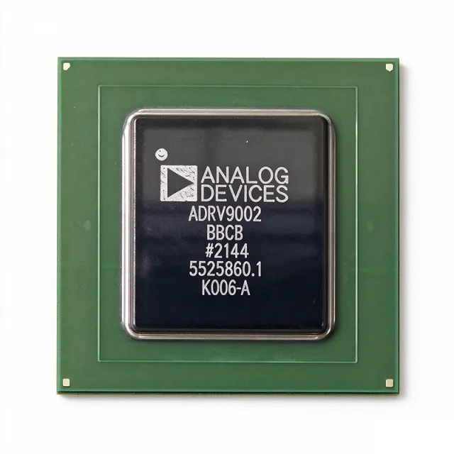
ADRV9002BBCZ-REEL - Dual RF Transceiver 30MHz-6GHz | Analog Devices
The ADRV9002BBCZ-REEL is a highly integrated, dual-channel RF transceiver from Analog Devices, designed for both narrow-band and wideband applications. It operates over a frequency range of 30 MHz to 6 GHz, making it suitable for a wide variety of wireless communication systems. The device integrates dual-channel transmitters, dual-channel receivers, synthesizers, and digital signal processing functions in a compact 196-ball TFBGA/CSPBGA package. This tape-and-reel variant is optimized for high-volume production. An RF transceiver is a device that combines both a transmitter and a receiver in a single package, sharing common circuitry. The ADRV9002 is a system-on-chip (SoC) that integrates the RF front-end, analog-to-digital converters (ADCs), digital-to-analog converters (DACs), and digital signal processing (DSP) blocks. This level of integration reduces component count, board space, and design complexity, making it ideal for software-defined radios (SDR) and other advanced wireless systems. Key features of the ADRV9002 include dual-channel operation, a wide frequency range of 30 MHz to 6 GHz, and support for both narrow-band and wideband signals. The device offers high linearity and dynamic range, ensuring reliable performance in demanding environments. It also includes integrated synthesizers, reducing the need for external PLLs and VCOs. The power output is 7.8 dBm, and the device operates from a single 3.3V supply. The ADRV9002 uses advanced CMOS technology to achieve high performance with low power consumption. The digital signal processing functions include filtering, gain control, and calibration, which are configurable via a serial peripheral interface (SPI). The device supports multiple operating modes, including TDD and FDD, and can be programmed for various bandwidths and sample rates. The integrated synthesizers provide low phase noise, essential for high-quality signal transmission and reception. Typical applications for the ADRV9002 include 5G NR base stations, small cells, macro cells, and other wireless infrastructure. It is also used in military and aerospace communications, radar systems, and test and measurement equipment. The wide frequency range and dual-channel capability make it a versatile choice for many RF designs. When designing with the ADRV9002, careful attention must be paid to power supply decoupling and thermal management. The device requires a clean 3.3V supply and adequate grounding to achieve optimal performance. The exposed pad on the package should be soldered to a thermal via array to dissipate heat effectively.
ADRV9003BBCZ - 1x1 RF Transceiver 30MHz-6GHz | Analog Devices
The ADRV9003BBCZ is a highly integrated, single-channel RF transceiver from Analog Devices, designed for a wide range of wireless applications. It operates from 30 MHz to 6 GHz, covering HF, VHF, UHF, and microwave bands, and features a single-channel transmitter, dual-channel receivers, integrated synthesizers, and extensive digital signal processing functions. The device is housed in a 196-pin CSP-BGA package, making it suitable for compact, high-performance designs. An RF transceiver is a device that combines a transmitter and a receiver in a single package, sharing common circuitry. It is a fundamental building block in wireless communication systems, enabling bidirectional data transfer over radio frequencies. The ADRV9003 integrates the RF front-end, analog-to-digital converters (ADCs), digital-to-analog converters (DACs), and digital signal processing, reducing the need for external components and simplifying system design. Key features of the ADRV9003 include a wide frequency range of 30 MHz to 6 GHz, a maximum sample rate of 61.44 MSPS, and high linearity and dynamic range. The device supports both FDD and TDD operation, making it versatile for various communication standards. It also includes integrated synthesizers and a digital interface, allowing for flexible configuration and control. The ADRV9003 utilizes advanced mixed-signal technology, integrating multiple functions that traditionally required separate components. Its architecture enables high performance while minimizing power consumption and board space. The device is designed for applications such as 5G base stations, software-defined radios, and test and measurement equipment, where high performance and flexibility are critical. Typical applications include 5G wireless infrastructure, point-to-point microwave links, and military communications. The wide frequency range and high dynamic range make it suitable for demanding environments. The device's integrated DSP functions allow for real-time signal processing, reducing the load on external processors. When designing with the ADRV9003, careful attention must be paid to power supply decoupling and thermal management. The device requires multiple supply rails, and proper filtering is essential to achieve optimal performance. The CSP-BGA package requires a well-designed PCB layout with adequate thermal vias to dissipate heat effectively.
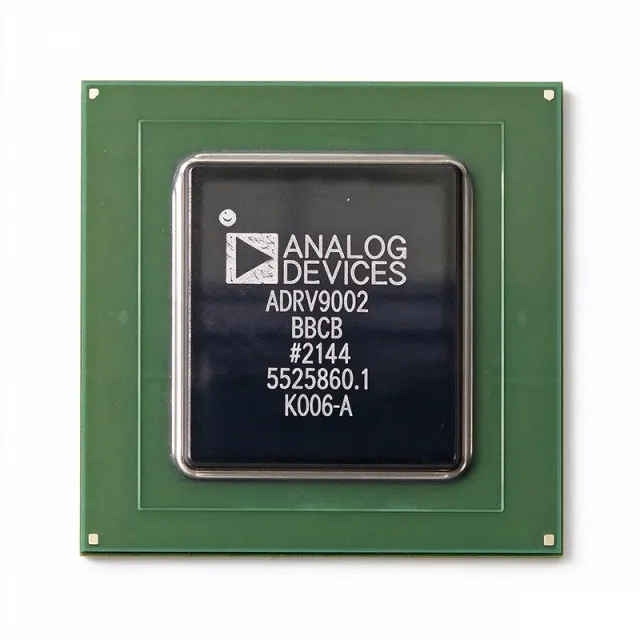
ADRV9003BBCZ-REEL - 30MHz-6GHz RF Transceiver | ADI
Analog Devices ADRV9003BBCZ-REEL is a highly integrated RF transceiver covering 30 MHz to 6 GHz, with a single-channel transmitter, dual-channel receivers, integrated synthesizers, and extensive digital signal processing functions. The device is supplied on tape and reel for high-volume surface-mount assembly and is part of the ADRV900x family used in wireless infrastructure and defense radio systems. The antenna is not included, so external antenna circuitry is required. An RF transceiver is a combined transmitter and receiver used in radio systems to convert between baseband digital data and modulated RF signals. In an ADRV9003-class transceiver, integrated synthesizers generate local-oscillator signals, while on-chip DSP performs filtering, gain control, calibration, and data formatting before handoff to an FPGA or SoC. This integration replaces multiple discrete IF/RF components and shortens radio design cycles. Key features of the ADRV9003BBCZ-REEL include the 30 MHz to 6 GHz operational range, 1T2R channel architecture, high linearity, high dynamic range, integrated synthesizers, and digital signal processing capabilities. According to the ADI product page, the device is optimized for high performance in demanding communications links. From an architecture perspective, the 1T2R configuration suits TDD systems that need one transmit path and two receive paths, such as base stations with receive diversity or dual-direction monitoring. The integrated DSP offloads many radio functions from the baseband processor, reducing host FPGA resource usage and supporting multiband software-defined radios. Typical applications include 5G/4G small cells, software-defined radios, phased-array radar feeds, industrial IoT gateways, satellite communications, and test-and-measurement instruments. In these systems, the device's bandwidth and linearity reduce error vector magnitude (EVM) and improve sensitivity. When designing with the ADRV9003BBCZ-REEL, pay attention to board-level thermal management for the BGA package and clean supply filtering near the RF pins. A well-controlled RF layout with proper impedance matching and grounding is essential to achieve the high dynamic range promised by the datasheet.
ADRV9004BBCZ - Dual RF Transceiver 30MHz-6GHz | Analog Devices
The ADRV9004BBCZ is a highly integrated, dual-channel RF transceiver from Analog Devices, designed for narrow-band and wideband applications. It operates over a frequency range of 30 MHz to 6 GHz, covering HF, VHF, UHF, and microwave bands. The device integrates dual-channel transmitters, dual-channel receivers, integrated synthesizers, and digital signal processing functions into a single 196-ball CSP_BGA package (12 mm × 12 mm). It supports configurable CMOS or LVDS serial synchronous interfaces (SSI) for high and low data rate communication. An RF transceiver is a device that combines a transmitter and receiver, sharing common circuitry or a single housing. In the hierarchy of wireless communication systems, an RF transceiver is a key component within the radio frequency front-end, which connects the antenna to the baseband processor. The ADRV9004BBCZ is a software-defined radio (SDR) solution, enabling flexible modulation schemes and frequency agility through digital control. Key features include dual-channel operation, wide frequency coverage, high linearity, and high dynamic range. The device supports both narrow-band and wideband signal processing, making it suitable for a variety of communication standards. It operates with 1.3V and 1.8V power supplies, and is available in a tray packaging. The ADRV9004BBCZ is RoHS compliant and is an active product in Analog Devices' portfolio. Technically, the ADRV9004BBCZ integrates multiple synthesizers, mixers, filters, and ADCs/DACs, providing a complete RF front-end solution. Its digital signal processing capabilities include filtering, gain control, and calibration algorithms, reducing the need for external components. The device is designed for high performance, with excellent noise figure and linearity, ensuring reliable communication in demanding environments. Typical applications include cellular base stations, point-to-point microwave links, satellite communications, and defense systems. Its wide frequency range and dual-channel capability make it ideal for MIMO and diversity schemes. The compact package and integrated functionality reduce board space and design complexity. When designing with the ADRV9004BBCZ, careful attention must be paid to power supply decoupling and thermal management. The device's thermal resistance values are specified per JEDEC standards (JESD51-12), and proper PCB layout with adequate ground planes is essential for optimal RF performance.

ADRV9004BBCZ-REEL - Dual RF Transceiver 30MHz-6GHz | Analog Devices
The ADRV9004BBCZ-REEL is a highly integrated, dual-channel RF transceiver from Analog Devices, designed for a wide range of wireless applications. It operates over a frequency range of 30 MHz to 6 GHz, making it suitable for both narrow-band and wideband communication systems. The device integrates dual-channel transmitters, dual-channel receivers, integrated synthesizers, and digital signal processing functions into a single 196-ball CSP_BGA package, offering a compact solution for space-constrained designs. An RF transceiver is a device that combines both transmit and receive functions in a single module, enabling bidirectional communication over radio frequencies. In the hierarchy of wireless communication, an RF transceiver sits between the baseband processor and the antenna, handling the conversion of digital data to RF signals for transmission and RF signals to digital data for reception. The ADRV9004 belongs to the family of software-defined radio (SDR) transceivers, which allow flexible configuration of frequency, bandwidth, and modulation schemes via software, making them ideal for multi-standard and multi-band systems. Key features of the ADRV9004BBCZ-REEL include dual-channel operation, a wide frequency range from 30 MHz to 6 GHz, and a maximum output power of 7.8 dBm. The device supports both CMOS and LVDS serial synchronous interfaces (SSI) for high data rate and low data rate communication with baseband processors. Its high linearity and dynamic range ensure reliable performance in demanding environments, while the integrated synthesizers reduce external component count and simplify design. Technically, the ADRV9004 employs advanced mixed-signal processing, including digital filtering and calibration algorithms, to optimize performance across its operating range. The device is packaged in a 12 mm × 12 mm, 196-ball chip scale package ball grid array (CSP_BGA), which provides excellent thermal and electrical performance. The REEL suffix indicates tape-and-reel packaging, suitable for automated assembly in high-volume production. Typical applications include 5G NR small cells, point-to-point microwave links, satellite communications, and test and measurement equipment. The wide frequency range and dual-channel capability make it a versatile choice for both commercial and industrial wireless systems. When designing with the ADRV9004, careful attention must be paid to power supply decoupling and PCB layout to maintain signal integrity and minimize noise. The device requires multiple supply rails, and proper filtering is essential to achieve the specified performance.
ADRV9009BBCZ - Dual RF Transceiver 75MHz-6GHz | Analog Devices
The ADRV9009BBCZ is a highly integrated, radio frequency (RF), agile transceiver from Analog Devices, offering dual transmitters and receivers, integrated synthesizers, and digital signal processing functions. It operates over a frequency range of 75 MHz to 6 GHz, making it suitable for a wide variety of wireless applications. The device is housed in a 196-pin CSP-BGA package and is designed for surface mount assembly. An RF transceiver is a device that combines both a transmitter and a receiver in a single package, enabling bidirectional communication over radio frequencies. The ADRV9009 is a key component in modern wireless systems, providing the analog and digital signal processing needed to convert between baseband data and RF signals. It integrates multiple functions such as filtering, amplification, and frequency synthesis, reducing the need for external components and simplifying system design. Key features of the ADRV9009BBCZ include support for 3G, 4G, and 5G macro cell time division duplex (TDD) base station applications, dual transmitters and receivers, and an observation receiver for transmit monitoring. The device also includes integrated synthesizers and digital signal processing, enabling high performance with low power consumption. The operating temperature range is -40°C to +85°C, and the device is RoHS compliant. The ADRV9009 utilizes advanced mixed-signal processing to achieve high dynamic range and low noise, essential for demanding cellular infrastructure applications. Its agile frequency synthesis allows rapid hopping across the 75 MHz to 6 GHz band, supporting multi-band and multi-standard radios. The integrated digital signal processing offloads the baseband processor, reducing system complexity and power consumption. Typical applications include 3G/4G/5G macro cell base stations, small cells, and other wireless infrastructure. The device is also used in phased array radar, satellite communications, and test and measurement equipment. Its wide frequency range and high integration make it a versatile choice for many RF systems. When designing with the ADRV9009, careful attention must be paid to power supply decoupling and thermal management. The device requires multiple supply rails (1.3V, 1.8V, 1.89V) and a well-designed PCB layout to achieve optimal performance. Reference designs and evaluation boards are available from Analog Devices to accelerate development.
ADRV9009BBCZ-REEL - Dual RF Transceiver 75MHz-6GHz | Analog Devices
The ADRV9009BBCZ-REEL is a highly integrated, radio frequency (RF), agile transceiver from Analog Devices, offering dual transmitters and receivers, integrated synthesizers, and digital signal processing functions. It operates over a frequency range of 75 MHz to 6 GHz, making it suitable for a wide variety of wireless applications. The device is packaged in a 196-pin CSP-BGA and is provided in tape and reel packaging for automated assembly. An RF transceiver is a device that combines both a transmitter and a receiver in a single package, sharing common circuitry. The ADRV9009 is a system-on-chip (SoC) that integrates the RF front-end, mixed-signal converters, and digital signal processing, reducing the need for external components. It is part of the broader category of radio frequency integrated circuits (RFICs), which are essential for modern wireless communication systems. Key features of the ADRV9009 include dual-channel operation, support for frequency division duplexing (FDD) and time division duplexing (TDD), and a JESD204B interface for high-speed data transfer to FPGAs or processors. The device also includes observation receivers (ORx) for digital predistortion and monitoring, and it supports a wide bandwidth of up to 200 MHz per channel. The integrated synthesizers and clock management simplify system design. Technically, the ADRV9009 employs advanced mixed-signal processing, including high-speed ADCs and DACs, and digital filters. It operates from multiple supply rails (1.3V, 1.8V, 1.89V) and includes power management features. The device is designed for high linearity and low noise, ensuring excellent signal quality. Its flexible architecture allows configuration for various standards, including 2G/3G/4G/5G cellular, and it is also used in military and aerospace applications. Typical applications include cellular base stations, small cells, phased array radar, and software-defined radio (SDR) systems. The ADRV9009's wide frequency range and dual-channel capability make it ideal for MIMO and diversity schemes. It is also used in test and measurement equipment and satellite communications. When designing with the ADRV9009, careful attention must be paid to power supply decoupling and thermal management. The device's high integration requires a well-designed PCB layout to minimize noise and ensure stable operation. The JESD204B interface simplifies data transfer but requires proper clocking and synchronization.
ADSY1100 - 4Tx/4Rx 20GSPS RF Digitizer | Analog Devices
The Analog Devices ADSY1100 is a fully integrated ultra-wideband, multichannel RF transceiver and processing system-on-module (SOM) in a 3UVPX SOSA-aligned format. It is built around ADI's next-generation "Apollo" MXFE product (AD9084), featuring DAC sample rates up to 28 GSPS and ADC sample rates up to 20 GSPS in a 4Tx/4Rx configuration. The module supports RF frequencies from 0.1 GHz to 20 GHz, making it a versatile solution for wideband signal acquisition and generation. An RF digitizer is a system that converts analog RF signals into digital data for processing, often incorporating tuners, ADCs, DACs, and digital signal processing. The ADSY1100 integrates these functions into a compact 3UVPX form factor, enabling rapid system integration for defense, aerospace, and communications applications. As a system-on-module, it combines the RF front-end, data converters, and processing capabilities, reducing development time and system complexity. Key features include 4 transmit and 4 receive channels, support for 100Gb optical data links for high-speed external data transfer, and a VITA 65 slot profile for standardized backplane integration. The module is designed for high-density, multi-channel systems where space and power efficiency are critical. Its wide frequency range and high sample rates enable direct RF sampling, eliminating the need for multiple downconversion stages. The ADSY1100 leverages the AD9084 MXFE, which integrates high-speed DACs and ADCs with digital signal processing blocks. This architecture provides flexibility in configuring the system for various bandwidths and center frequencies. The 100Gb optical links allow seamless data streaming to external processors or FPGAs, supporting real-time signal processing and analysis. Typical applications include electronic warfare, radar systems, satellite communications, and spectrum monitoring. The module's wideband capability and high dynamic range make it suitable for capturing and analyzing complex RF environments. Its SOSA-aligned format ensures interoperability with other SOSA-compliant modules, facilitating system upgrades and maintenance. When designing with the ADSY1100, consider the thermal management requirements due to the high-speed converters and processing elements. Adequate cooling and power supply decoupling are essential for reliable operation. The module's backplane interface follows the VITA 65 standard, ensuring proper mechanical and electrical integration.
AS22010P - 10GBASE-T Multi-Rate Ethernet PHY | Aeonsemi
The Aeonsemi AS22010P is a 2nd generation, low-power, multi-rate single-port physical layer transceiver (PHY) supporting 10GBASE-T, 5GBASE-T, 2.5GBASE-T, 1000BASE-T, 100BASE-TX, and 10BASE-Te. It is part of Aeonsemi's ChronoPHY™ family, an Ethernet PHY architecture optimized for low-jitter and low-latency operation in time-sensitive networking applications such as wireless infrastructure, AI edge, industrial automation, and real-time Ethernet systems. The device is offered in a 7 mm × 7 mm BGA package and is specified across the industrial temperature range of -40 °C to +85 °C. An Ethernet PHY (physical layer transceiver) is the analog front-end and digital encoding block that connects a MAC controller to a copper twisted-pair cable. Multi-rate PHYs like the AS22010P auto-negotiate among several IEEE 802.3 speeds on the same RJ45 port, allowing platform designers to upgrade from Gigabit Ethernet to multi-gigabit without changing the magnetics or PCB footprint. Within the broader hierarchy, the AS22010P sits as: Ethernet PHY → physical layer transceiver → network interface IC → wired-connectivity semiconductor. The ChronoPHY™ architecture prioritizes low-jitter clock recovery and PTP/1588 timestamping accuracy to support deterministic networking for AI edge and Wi-Fi 7 backhaul. Key features include support for NBASE-T and MGBASE-T multi-gig rates (2.5G/5G alongside 10G), extended cable reach beyond the IEEE 802.3 baseline of 55 m on Cat6A, advanced EMC and interference immunity, integrated PTP/1588 timing features, and approximately 40% lower power than the prior generation AS21010P. The BGA package provides a compact 7 mm × 7 mm footprint suitable for high-density switch and NIC designs where PCB real estate is at a premium. Typical applications include Wi-Fi 7 access-point uplinks, AI-edge inference gateways, multi-gigabit NAS platforms, AV-over-IP bridges, industrial TSN switches, and 10GBASE-T NIC cards. Designers migrating from the first-generation AS21010P can drop the AS22010P into the same board layout while gaining lower power, improved timing accuracy, and extended cable reach. For deterministic AI edge and wireless-infrastructure deployments, the AS22010P's low-jitter clock path directly improves MAC-to-PHY timestamp fidelity, a critical parameter for 5G fronthaul and TSN workflows. When designing with the AS22010P, observe the BGA PCB-layout recommendations in the datasheet (microvia stack-up, matched 100-ohm differential impedance, and integrated magnetic-module footprint) to preserve EMC performance across the full 100 m cable reach. This page synthesizes manufacturer documentation, second-generation release data, and parameter-by-parameter comparisons not consolidated on any single manufacturer page.