RF & Wireless
ژێرپۆلەکان
بەرهەمەکان (730+)

AD9361BBCZ-CSL - RF Agile Transceiver, 70MHz-6GHz | Analog Devices
The AD9361BBCZ-CSL is a high-performance, highly integrated RF Agile Transceiver from Analog Devices, designed for 3G and 4G base station applications. It operates over a frequency range of 70 MHz to 6 GHz and features a 2x2 transceiver architecture with integrated frequency synthesizers, making it ideal for a broad range of radio transceiver applications. The device is housed in a 144-ball CSPBGA package and is qualified for space applications, with radiation testing for Total Ionizing Dose (TID) effects and enhanced reliability for aerospace environments. An RF transceiver is a device that combines a transmitter and receiver in a single package, handling both the modulation/demodulation of signals and the conversion between RF and baseband frequencies. The AD9361BBCZ-CSL integrates the RF front end, mixed-signal baseband, and frequency synthesizers, simplifying design-in and reducing component count. This integration is part of a hierarchy: RF transceiver -> RF front end -> mixed-signal baseband -> frequency synthesizer -> radio communication system. Key features include a wide frequency range of 70 MHz to 6 GHz, support for channel bandwidths from 200 kHz to 56 MHz, and a 12-bit ADC/DAC resolution. The device offers programmable gain control, digital filtering, and a flexible digital interface supporting CMOS and LVDS standards. Its high level of integration eliminates the need for external VCOs and loop filters, reducing board space and design complexity. Technically, the AD9361BBCZ-CSL uses a direct-conversion architecture with integrated fractional-N synthesizers, achieving excellent phase noise and linearity. The device supports both FDD and TDD modes, making it versatile for various wireless standards. Its radiation-hardened design ensures reliable operation in space environments, with TID testing and enhanced screening. Typical applications include 3G/4G base stations, software-defined radios (SDR), military and aerospace communications, and point-to-point microwave links. The wide frequency range and programmability make it suitable for multi-band, multi-standard radios. When designing with this device, careful attention must be paid to power supply decoupling and PCB layout to maintain optimal RF performance. The device requires multiple supply rails and a clean reference clock for best results.
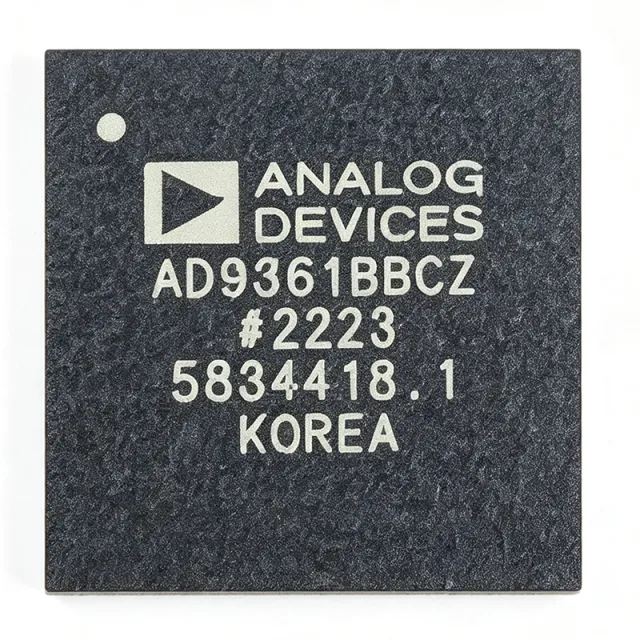
AD9361BBCZ-REEL - 70MHz-6GHz RF Agile Transceiver | Analog Devices
The AD9361BBCZ-REEL is a high performance, highly integrated radio frequency (RF) Agile Transceiver from Analog Devices, designed for 3G and 4G base station applications. It operates over a frequency range of 70 MHz to 6 GHz, covering a wide spectrum of cellular and other wireless standards. The device integrates a 2x2 transceiver architecture with configurable 12-bit CMOS/LVDS digital baseband interface, enabling flexible connection to baseband processors. Housed in a 144-ball CSPBGA package, it offers a compact solution for multi-band, multi-standard radio designs. An RF transceiver is a device that combines both a transmitter and a receiver, sharing common circuitry. The AD9361 is an agile transceiver, meaning it can be dynamically reconfigured to support different frequency bands, channel bandwidths, and modulation schemes. This flexibility makes it a key component in software-defined radio (SDR) systems, where the same hardware can adapt to various communication standards without redesign. The AD9361 sits at the heart of the RF front-end, bridging the antenna and the digital baseband processor, and is essential for modern wireless infrastructure. Key features include a frequency range of 70 MHz to 6 GHz, support for channel bandwidths from less than 200 kHz to 56 MHz, and a highly linear receiver with noise figure as low as 2 dB. The transmitter offers excellent error vector magnitude (EVM) performance, enabling high-order modulation schemes. The device also includes integrated fractional-N synthesizers, digital filters, and automatic gain control (AGC), reducing external component count and simplifying design. Technically, the AD9361 employs a direct conversion architecture with advanced calibration algorithms to mitigate I/Q imbalance and DC offset. It supports both FDD and TDD modes, and its programmable interface allows seamless integration with various baseband processors. The device operates from a 1.3V core supply and includes multiple power-down modes for efficient power management. Typical applications include 3G/4G base stations, small cells, software-defined radios, military communications, and test and measurement equipment. Its wide frequency range and programmability make it suitable for multi-band, multi-standard radio platforms. When designing with the AD9361, careful attention must be paid to power supply decoupling and PCB layout to achieve optimal RF performance. The device requires a clean 1.3V supply and proper grounding to minimize noise and interference.
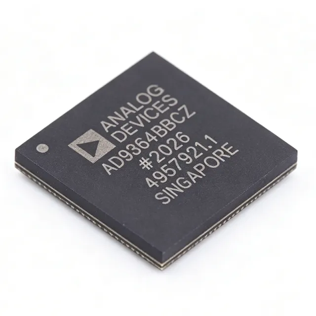
AD9364BBCZ - 70MHz-6GHz RF Agile Transceiver | Analog Devices
The AD9364BBCZ is a high-performance, highly integrated radio frequency (RF) Agile Transceiver™ from Analog Devices, designed for 3G and 4G base station applications. It operates from 70 MHz to 6.0 GHz, covering most licensed and unlicensed bands, and supports channel bandwidths from less than 200 kHz to 56 MHz. The device combines an RF front end with a flexible mixed-signal baseband section and integrated frequency synthesizers, simplifying design-in by providing a configurable digital interface to a processor. It is a 1x1 variant with 2 receive and 2 transmit paths, packaged in a 144-ball LFBGA/CSPBGA. An RF transceiver is a device that both transmits and receives radio frequency signals, integrating the RF front end, mixed-signal baseband, and frequency synthesis in a single IC. It sits between the antenna and the digital baseband processor in a communication system, converting RF signals to digital baseband and vice versa. The AD9364 is part of the RF Agile Transceiver family, which includes the AD9361 and AD9363, and is designed for software-defined radio (SDR) applications. Key features include wide frequency coverage (70 MHz to 6 GHz), programmable channel bandwidth (200 kHz to 56 MHz), integrated synthesizers, and a configurable digital interface. The device supports FDD and TDD modes, and includes auxiliary ADC/DACs for monitoring and control. Its high integration reduces external component count and board space, making it ideal for compact base station designs. The AD9364 uses a direct-conversion architecture with integrated filters and gain control, providing excellent linearity and sensitivity. It includes a dual-channel receiver and transmitter, with support for MIMO configurations when paired with multiple devices. The device is programmable via a 3- or 4-wire SPI interface, allowing dynamic reconfiguration of frequency, gain, and filter settings. Typical applications include 3G/4G base stations, software-defined radio, point-to-point microwave links, and test and measurement equipment. Its wide frequency range and bandwidth flexibility make it suitable for both licensed and unlicensed band operation. When designing with the AD9364, careful attention must be paid to power supply decoupling and RF layout to achieve optimal performance. The device requires multiple supply rails and a clean reference clock. Proper grounding and shielding are essential to minimize noise and interference.
AD9364BBCZ-REEL - 70MHz-6GHz RF Agile Transceiver | Analog Devices
The AD9364BBCZ-REEL is a high-performance, highly integrated RF Agile Transceiver™ from Analog Devices, designed for a broad range of wireless applications. It operates from 70 MHz to 6.0 GHz, covering most licensed and unlicensed bands, and supports channel bandwidths from less than 200 kHz to 56 MHz. The device integrates an RF front end, a flexible mixed-signal baseband section, and frequency synthesizers, simplifying design-in by providing a configurable digital interface to a processor. This 1x1 variant features one receive and one transmit channel, making it ideal for single-channel transceiver designs. An RF transceiver is a device that combines both a transmitter and a receiver in a single package, handling the modulation, demodulation, and frequency conversion of RF signals. It is a critical component in wireless communication systems, bridging the analog RF domain and the digital baseband processor. The AD9364 belongs to the RF Agile Transceiver family, which includes the AD9361 (2x2) and AD9363 (1x1, reduced bandwidth), all sharing a similar architecture and programming model. Key features of the AD9364 include a wide frequency range of 70 MHz to 6 GHz, support for channel bandwidths from 200 kHz to 56 MHz, and a configurable digital interface (CMOS/LVDS) for baseband connectivity. The device offers excellent receiver sensitivity and transmitter linearity, with an output power of 8 dBm. It also includes integrated fractional-N synthesizers, reducing external component count and simplifying frequency planning. Technically, the AD9364 employs a direct-conversion architecture with advanced calibration algorithms to minimize I/Q imbalance and DC offset. The device supports both FDD and TDD modes, making it versatile for various wireless standards. Its programmability allows dynamic reconfiguration of frequency, bandwidth, and gain, enabling software-defined radio (SDR) implementations. Typical applications include 3G/4G base stations, software-defined radios, portable test equipment, and military communications. The wide frequency range and bandwidth flexibility make it suitable for multi-standard radios that must operate across different bands. When designing with the AD9364, careful attention must be paid to power supply decoupling and clocking. The device requires multiple supply rails, and proper filtering is essential to achieve optimal performance. The digital interface should be configured for the appropriate voltage levels and data rate to match the baseband processor.
AD9371BBCZ - Dual RF Transceiver 300MHz-6GHz | Analog Devices
The AD9371BBCZ is a highly integrated, wideband RF transceiver from Analog Devices, designed for dual-channel transmitters and receivers with integrated synthesizers and digital signal processing functions. It operates over a frequency range of 300 MHz to 6 GHz, making it suitable for a wide variety of wireless applications. The device is packaged in a 196-ball LFBGA/CSPBGA (12 mm x 12 mm) and is part of the Mykonos family. An RF transceiver is a device that combines both a transmitter and a receiver in a single package, enabling bidirectional communication over radio frequencies. The AD9371 is a system-on-chip (SoC) that integrates the RF front-end, analog-to-digital converters (ADCs), digital-to-analog converters (DACs), and digital signal processing (DSP) blocks, reducing the need for external components and simplifying system design. It sits within the hierarchy of RF transceivers -> wideband transceivers -> software-defined radio (SDR) components. Key features include dual transmitters and receivers, support for TDD and FDD modes, and a digital interface that supports JESD204B serial data. The device offers high dynamic range and low power consumption, making it ideal for battery-powered and portable applications. It also includes an observation path for transmitter monitoring and calibration, enhancing system performance. Technically, the AD9371 integrates fractional-N synthesizers for local oscillator (LO) generation, reducing external LO circuitry. The device supports a maximum receiver bandwidth of 100 MHz and transmitter bandwidth of 250 MHz, enabling wideband operation. It operates from a 3.3V supply and includes power management features to optimize efficiency. Typical applications include software-defined radios, cellular base stations (3G/4G/5G), point-to-point microwave links, and military communications. Its wide frequency range and high integration make it a versatile choice for both commercial and defense systems. When designing with the AD9371, careful attention must be paid to power supply decoupling and thermal management, as the device dissipates significant power. The JESD204B interface requires proper clocking and synchronization to ensure data integrity.
AD9371BBCZ-REEL - Dual RF Transceiver 300MHz-6GHz | Analog Devices
The AD9371BBCZ-REEL from Analog Devices is a highly integrated, wideband RF transceiver designed for dual-channel transmitters and receivers, integrated synthesizers, and digital signal processing functions. Operating from 300 MHz to 6 GHz, this device supports a wide range of wireless communication standards, including 4G/5G cellular infrastructure, software-defined radio (SDR), and radar systems. The transceiver is housed in a 196-ball CSP_BGA package (12 mm × 12 mm), offering a compact solution for high-performance RF front-ends. An RF transceiver is a device that combines both a transmitter and a receiver in a single package, handling the modulation, demodulation, and frequency conversion of RF signals. In the hierarchy of wireless communication systems, an RF transceiver sits between the baseband processor and the antenna, converting digital baseband data to analog RF signals for transmission and vice versa for reception. The AD9371 integrates dual transmitters and receivers, along with observation and feedback paths, enabling advanced features like digital pre-distortion (DPD) and envelope tracking. Key features of the AD9371 include dual-channel transmitters and receivers, integrated synthesizers, and a digital signal processing block that supports various filtering and calibration functions. The device offers a high dynamic range and low noise figure, making it suitable for demanding applications. It also includes an observation receiver (ORx) path for DPD and a feedback path for transmit monitoring. The transceiver supports a wide frequency range, from 300 MHz to 6 GHz, covering most cellular and ISM bands. Technically, the AD9371 employs a direct-conversion architecture with advanced calibration algorithms to achieve high performance. It integrates fractional-N synthesizers for both transmit and receive paths, reducing external component count. The device operates from a 1.3 V core supply and 1.8 V I/O supply, with power dissipation typically around 5 W. The digital interface supports JESD204B, a high-speed serial interface standard, enabling efficient data transfer to FPGAs or ASICs. Typical applications include 4G/5G macro and small cell base stations, software-defined radios, phased array radar, and test and measurement equipment. The AD9371's wide frequency range and high integration make it ideal for multi-band, multi-standard systems where board space and power efficiency are critical. When designing with the AD9371, careful attention must be paid to power supply decoupling and thermal management. The device requires multiple supply rails, and proper filtering is essential to achieve the specified noise performance. The exposed pad on the CSP_BGA package should be soldered to a thermal via array to ensure adequate heat dissipation.
AD9375BBCZ - Dual RF Transceiver with DPD | Analog Devices
The AD9375BBCZ is a highly integrated, wideband radio frequency (RF) transceiver from Analog Devices, designed for 3G/4G/5G base stations and massive MIMO systems. It features dual-channel transmitters (Tx) and receivers (Rx), integrated synthesizers, a fully integrated digital predistortion (DPD) actuator and adaptation engine, and comprehensive digital signal processing functions. Operating from 300 MHz to 6 GHz, it supports a wide range of cellular and wireless standards. An RF transceiver is a device that combines both a transmitter and a receiver in a single package, sharing common circuitry. In the hierarchy of wireless communication systems, an RF transceiver is a key component within the RF front-end, which sits between the antenna and the baseband processor. It handles the conversion of RF signals to and from intermediate frequencies or baseband, enabling wireless communication. The AD9375 is a high-performance example, integrating DPD to enhance linearity and efficiency in power amplifiers. Key features include dual-channel operation, integrated DPD, and a frequency range of 300 MHz to 6 GHz. The device supports observation paths for DPD and includes digital signal processing functions such as filtering, gain control, and calibration. It is housed in a 196-ball LFBGA/CSPBGA package, suitable for compact base station designs. The integrated DPD engine reduces the need for external DPD components, simplifying system design and reducing bill of materials. Technically, the AD9375 uses a direct conversion architecture with high dynamic range and linearity. It includes multiple PLLs and synthesizers for flexible frequency planning. The DPD actuator and adaptation engine work together to correct power amplifier nonlinearities, improving system efficiency and reducing spectral regrowth. The device also supports MIMO configurations, making it ideal for advanced antenna systems. Typical applications include 3G/4G/5G base stations, massive MIMO systems, software-defined radios, and military communications. Its wide frequency range and DPD capability make it suitable for both FDD and TDD systems. When designing with the AD9375, careful attention must be paid to power supply decoupling and thermal management. The device requires multiple supply rails and a well-designed PCB layout to achieve optimal performance. The integrated DPD engine requires configuration and calibration, which can be done via the serial peripheral interface (SPI).
AD9375BBCZ-REEL - Dual RF Transceiver with DPD | Analog Devices
The AD9375BBCZ-REEL is a highly integrated, dual RF transceiver from Analog Devices, designed for cellular and wireless infrastructure applications. It operates over a frequency range of 300 MHz to 6 GHz, covering a wide spectrum of communication bands. The device integrates two independent transmit and receive channels, along with an observation path for digital predistortion (DPD) and a sniffer receiver for spectrum monitoring. It is housed in a 196-ball LFBGA/CSPBGA package, offering a compact solution for multi-band, multi-standard transceiver designs. An RF transceiver is a device that combines both a transmitter and a receiver in a single package, handling the modulation, demodulation, and frequency conversion of RF signals. In modern communication systems, RF transceivers are essential components in base stations, small cells, and other wireless infrastructure, enabling high-speed data transmission and reception. The AD9375 belongs to the family of wideband transceivers, which are characterized by their ability to handle multiple frequency bands and communication standards, such as LTE, 5G NR, and WCDMA, with a single hardware platform. Key features of the AD9375 include its wide frequency range, dual-channel architecture, and integrated DPD capability. The DPD functionality allows for linearization of power amplifiers, improving efficiency and reducing distortion. The device also features a high dynamic range, with a receiver noise figure of [DATA_NEEDED: receiver noise figure] and a transmitter error vector magnitude (EVM) of [DATA_NEEDED: transmitter EVM]. It supports a maximum bandwidth of [DATA_NEEDED: maximum bandwidth] per channel, making it suitable for carrier aggregation and high-throughput applications. Technically, the AD9375 is built on a highly integrated architecture that includes mixers, filters, ADCs, DACs, and digital signal processing blocks. It uses a direct conversion architecture for both transmit and receive paths, minimizing external components and simplifying the design. The device is controlled via a serial peripheral interface (SPI), allowing for flexible configuration of frequency, gain, and filtering. It also includes a digital interface for baseband data transfer, supporting JESD204B standard for high-speed serial data transmission. Typical applications for the AD9375 include 4G/5G base stations, small cells, massive MIMO systems, and software-defined radios. Its wide frequency range and high performance make it ideal for multi-band, multi-standard transceivers, reducing the need for multiple discrete components. The integrated DPD capability is particularly beneficial in power amplifier linearization, improving system efficiency and reducing power consumption. When designing with the AD9375, it is important to consider the power supply requirements and thermal management. The device requires multiple supply rails, including 1.3V and [DATA_NEEDED: other supply voltages], and dissipates significant power, especially when operating at high output power. Proper PCB layout, including adequate grounding and decoupling, is critical to achieve optimal performance. Additionally, the JESD204B interface requires careful attention to clocking and synchronization to ensure reliable data transfer.
ADAR1000 - 8-16GHz 4-Channel Beamformer | Analog Devices
The ADAR1000 is a 4-channel, X band and Ku band beamforming core chip for phased arrays, operating from 8 GHz to 16 GHz. It is designed for half-duplex operation between receive and transmit modes, making it ideal for advanced radar and communication systems. The device is fabricated in a silicon-germanium, bipolar CMOS (BiCMOS) process and is available in a compact 88-terminal, 7 mm × 7 mm LGA package, specified from −40°C to +85°C. A beamforming IC is a specialized RF component that controls the phase and amplitude of signals in an antenna array to steer the beam electronically without moving parts. It is a key building block in phased array systems, which are used in radar, satellite communication, and 5G networks. The ADAR1000 integrates four channels, each with phase and gain control, enabling precise beam steering in both transmit and receive paths. Key features include 4-channel operation, half-duplex T/R switching, SPI control interface, and support for daisy-chaining multiple devices for larger arrays. The device offers high integration, reducing the component count and simplifying the design of phased array front-ends. Its wide frequency range covers both X band (8-12 GHz) and Ku band (12-16 GHz), providing flexibility for various applications. The ADAR1000 uses a BiCMOS process that balances high-frequency performance with low power consumption. The LGA package is designed for RF performance, with careful attention to thermal and electrical characteristics. The device includes on-chip registers for configuration, which can be programmed via SPI, and supports both SPI and T/R pin control modes. Typical applications include phased array radar, satellite communication, 5G beamforming, and electronic warfare systems. The ADAR1000 is also used in test and measurement equipment for beamforming validation. Its ability to daisy-chain up to four devices on a single evaluation board makes it scalable for larger arrays. When designing with the ADAR1000, it is critical to follow the recommended PCB layout and thermal management guidelines, as the LGA package requires specific footprint and stackup considerations. The device's SPI interface allows for flexible control, but careful attention must be paid to register programming to ensure proper operation.
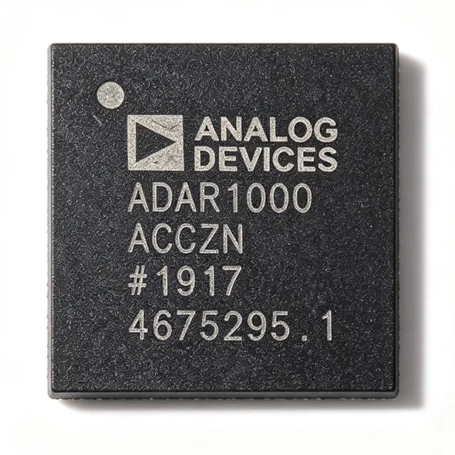
ADAR1000ACCZN - 8-16GHz 4-Ch X/Ku Beamformer | Analog Devices
The Analog Devices ADAR1000ACCZN is a 4-channel, 8 GHz to 16 GHz, X and Ku band beamforming core chip for phased array radar systems, packaged in a compact CC-88-1 chip-scale package. Operating in half-duplex between receive and transmit modes, it integrates full phase and gain control on all four channels with a single common RF_IO port. A beamformer IC is the core signal-routing element of an electronically steered antenna array. In a phased array system, each radiating element is driven by a beamformer channel that applies a calculated phase shift and gain weighting; by varying these weights across the array, the antenna beam is steered electronically without any mechanical movement. The ADAR1000 belongs to the RF transceiver and beam-steering hierarchy of microwave integrated circuits, sitting between the antenna elements and the transceiver or waveform generator. Key features of the ADAR1000 include four independent receive and transmit channels covering the full 8 GHz to 16 GHz band, digitally controlled phase shifting in 360-degree range with fine LSB resolution, per-channel gain control for amplitude tapering, and bidirectional operation through a common RF_IO pin that connects directly to the antenna element. The half-duplex TDD architecture simplifies the front-end by eliminating separate transmit and receive signal paths to the radiator. Technically, in receive mode input signals from four antenna elements pass through the four receive channels, where phase and amplitude are adjusted, and are combined at the common RF_IO port. In transmit mode, the RF_IO input signal is split and passes through the four transmit channels to the radiating elements. Control of all gain, phase, and T/R state is performed through a serial peripheral interface (SPI), enabling rapid beam reconfiguration under FPGA or microprocessor control. Typical applications include X band and Ku band phased array radar for defense and aerospace platforms, satellite communications terminals, and electronic warfare systems requiring high-resolution beam steering. When designing with the ADAR1000, pay close attention to supply sequencing, RF board layout for the chip-scale package, and thermal management, since beamformer ICs in dense arrays operate in thermally constrained enclosures. This page synthesizes distributor availability, datasheet references, and practical design guidance not found on any single manufacturer or distributor page.
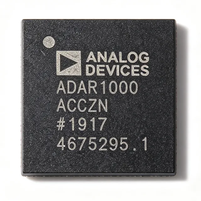
ADAR1000ACCZN-R7 - 8-16GHz 4-Ch X/Ku Beamformer | Analog Devices
The Analog Devices ADAR1000ACCZN-R7 is a 4-channel, 8 GHz to 16 GHz X-band and Ku-band beamforming core chip for phased array radar systems, housed in an 88-pin LGA exposed-pad package supplied in tape and reel (-R7) format. A beamformer core chip is an RF integrated circuit that provides independent amplitude and phase control per channel, enabling electronic steering of a phased array antenna without mechanical movement. Within the RF signal chain hierarchy, the ADAR1000 sits between the transceiver and the antenna elements, functioning as the vector-modulating T/R module that shapes the beam. Beamformers like the ADAR1000 are foundational building blocks of modern active electronically scanned array (AESA) architectures used in radar and communication systems. Key features include 4 fully independent receive and transmit channels covering 8 GHz to 16 GHz, half-duplex operation with fast transmit/receive switching controlled by a single pin, and per-channel programmable phase and gain. The device integrates the complete beamforming function - low noise amplification in receive mode, power amplification in transmit mode, and vector modulation on every channel - reducing board area and component count dramatically versus discrete implementations. Architecturally, in receive mode input signals pass through the four receive channels and are combined at the common RF_IO pin; in transmit mode the RF_IO input signal is split and passes through the four transmit channels. All on-chip registers are controlled through a simple 4-wire serial port interface (SPI), and two address pins allow SPI control of up to four ADAR1000 devices on the same serial lines, simplifying large array designs. Dedicated transmit and receive load pins provide synchronization of all ADAR1000 chips in the same array. Typical applications include X-band and Ku-band phased array radar, satellite communication terminals, and multi-beam antenna systems where compact size, precise phase/gain control, and channel-to-channel synchronization are required. Design consideration: because the four channels share the common RF_IO port, PCB symmetry between channels is important for maintaining amplitude and phase tracking across the array. This page synthesizes distributor availability data, packaging details, and application guidance not consolidated in the manufacturer datasheet alone.
ADAR4002 - 0.5-19GHz Bidirectional TDU | Analog Devices
The ADAR4002 is a low power, broadband, bidirectional, single-channel IC designed for applications requiring programmable time delay and/or attenuation. It operates from 0.5 GHz to 19 GHz, with both RF1 and RF2 ports internally matched to 50 Ω. The device integrates a true time delay unit (TDU) and a digital step attenuator (DSA) in a single package, providing flexible digital control via SPI or shift register interface. The ADAR4002 is available in a 14-lead WFDFN exposed pad package (ACPZ), making it suitable for compact RF front-end designs. A true time delay unit (TDU) is a component that introduces a controlled delay to an RF signal, independent of frequency, which is essential for phased array beamforming and time-domain applications. Unlike phase shifters that only adjust phase, a TDU preserves signal integrity across wide bandwidths, making it critical for wideband systems. The ADAR4002 combines TDU and DSA functions, reducing component count and simplifying system design. Key features include a wide operating frequency range of 0.5 GHz to 19 GHz, bidirectional operation, and low power consumption. The device supports both SPI and shift register control, with on-chip memory for 32 TDU and DSA states. The integrated sequencers allow fast bidirectional memory advance via the UPDATE pin, enabling rapid state changes. The 50 Ω matched ports simplify system integration, and the compact 14-lead WFDFN package supports space-constrained designs. Technically, the ADAR4002 uses a combination of switched delay lines and attenuator stages to achieve precise time delay and attenuation. The bidirectional design allows signal flow in either direction, making it versatile for T/R modules. The SPI interface enables daisy chaining of multiple devices, and the shift register mode provides a simple parallel control option. The device operates over a wide temperature range, ensuring reliability in demanding environments. Typical applications include phased array radar, electronic warfare, 5G beamforming, and test and measurement equipment. The wideband operation and bidirectional capability make it ideal for T/R modules in defense and communication systems. The low power consumption is beneficial for portable and battery-operated systems. When designing with the ADAR4002, ensure proper RF layout and decoupling to maintain performance. The exposed pad should be soldered to a ground plane for thermal and electrical performance. The control interface should be configured according to system requirements, and the memory states should be programmed to achieve the desired delay and attenuation values.
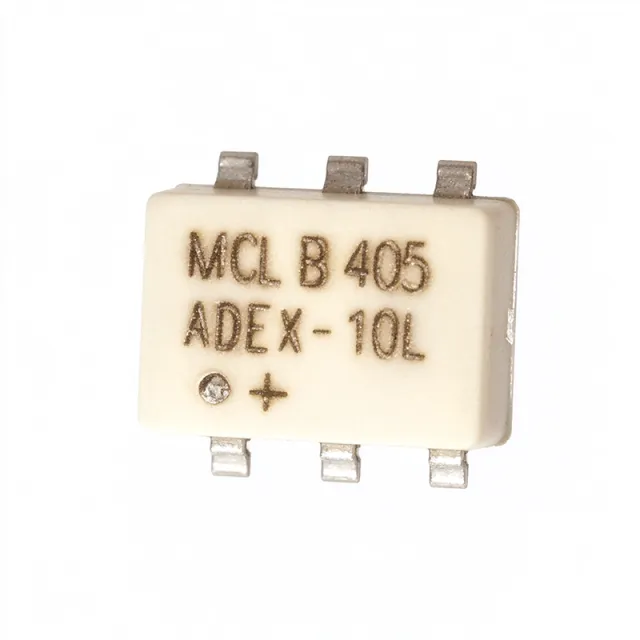
ADEX-10L+ - 10-1000 MHz SMT Double Balanced Mixer | Mini-Circuits
The Mini-Circuits ADEX-10L+ is a Level-4 surface-mount double-balanced RF mixer covering RF and LO frequencies from 10 MHz to 1000 MHz with an IF bandwidth from DC to 1000 MHz. It is housed in a Mini-Circuits low-profile ceramic-compatible SMT package (case style FV1201A-1) and is rated for 50 mW RF input power and 40 mA DC current. The "+" suffix denotes RoHS-compliant lead-free terminations. A double-balanced mixer (DBM) is a passive frequency-translation building block that multiplies two input signals (RF and LO) to produce sum and difference products at the IF port. By using a diode ring or balun-based topology, the DBM suppresses the LO signal at the RF and IF ports and rejects even-order intermodulation products, providing high port-to-port isolation and excellent spurious performance. The ADEX-10L+ family of mixers is widely used in upconverters, downconverters, modulators, demodulators, and phase detectors in both commercial and industrial RF subsystems. Key specifications include typical LO-RF isolation of 35 dB (midband), conversion loss around 8 dB typical, IP3 in the +13 to +17 dBm range, and 1 dB compression point near +1 dBm. Operating temperature ranges from -40°C to +85°C, with a storage range of -55°C to +100°C. The SMT construction eliminates the need for hand-wiring of traditional TO-style mixers and is compatible with automated reflow and pick-and-place assembly. Typical applications include HF/VHF/UHF receiver front-ends, frequency-agile signal generators, RF power monitors, cable-television (CATV) infrastructure, software-defined radio (SDR) platforms, instrumentation, and laboratory test equipment. Its wide 10-1000 MHz RF/LO band makes it a versatile general-purpose mixer for both narrowband and broadband signal chains. Compared to active mixer ICs, the ADEX-10L+ offers higher linearity (IP3) at the expense of requiring external LO drive and DC bias considerations. When designing with the ADEX-10L+, pay close attention to LO drive level (typically +7 dBm to +13 dBm), port impedance matching to 50 ohms, and IF filtering to remove image and LO-leakage products. Surface-mount mixers require careful PCB layout with controlled-impedance traces and solid ground planes to achieve rated isolation and conversion-loss performance. Use of balun transformers or balanced amplifier chains upstream improves overall system noise figure. This page synthesizes distributor pricing, validated drop-in alternatives, and practical PCB/layout design notes not found in the manufacturer datasheet, giving engineers a one-stop reference for the ADEX-10L+.

ADF4116BRU - 550 MHz Integer-N RF PLL | Analog Devices
The Analog Devices ADF4116BRU is a single-band integer-N phase-locked-loop frequency synthesizer with a 550 MHz operating ceiling, a programmable RF prescaler, and a three-wire serial interface, housed in a 16-lead TSSOP package. It is designed to generate stable local-oscillator signals for wireless receivers and transmitters. A frequency synthesizer is a clock-and-timing device that locks an output frequency to a stable reference. The ADF4116 family belongs to the broader RF PLL hierarchy: a phase-frequency detector and precision charge pump compare the divided output with a reference signal, while programmable counters determine the multiplication ratio. This architecture provides programmable frequency generation for RF upconversion, downconversion, modulation, and test equipment. Key features identified in the verified manufacturer data include a 550 MHz maximum operating frequency, a 32/33 dual-modulus prescaler, a 5-bit A counter, a programmable B counter, selectable charge-pump currents, and digital lock detect. The device supports a 5.5 V power supply and a separate VP connection that can extend the tuning-voltage range in suitable 3 V systems. Its serial programming interface simplifies frequency, counter, prescaler, and power-state configuration. Technically, the integer-N architecture uses a dual-modulus prescaler to synthesize many output frequencies from one reference source. The programmable A and B counters divide the prescaled RF signal, while the phase-frequency detector controls the charge-pump current applied to an external loop filter. Correct loop-filter design, reference stability, and RF layout determine practical phase noise and lock performance; the supplied search results do not provide complete phase-noise curves or timing values. Typical uses include wireless receiver and transmitter local oscillators, upconversion and downconversion chains, industrial RF systems, instrumentation, and communication equipment. The 16-TSSOP package is compact and surface-mountable, but exposed-pad thermal details and exact pin names were not provided in the verified data. When replacing this part, verify the complete ADF4116 datasheet pinout, counter limits, reference frequency, prescaler range, supply sequencing, and loop-filter requirements. The verified distributor result also identifies ADF4116BRUZ as the current production variant with identical electrical specifications and pin compatibility, but that claim is not treated as a manufacturer-confirmed drop-in substitute here. This page combines the verified manufacturer and distributor records with engineering guidance, application context, and replacement caveats for engineers evaluating RF PLL layouts.

ADF4150BCPZ-RL7 - 4.4GHz Fractional-N PLL Synthesizer | Analog Devices
The Analog Devices ADF4150BCPZ-RL7 is a fractional-N or integer-N frequency synthesizer IC for RF phase-locked-loop designs, operating up to 4.4 GHz in a 24-lead WFQFN exposed-pad package. The device works with an external voltage-controlled oscillator, loop filter, and reference frequency, providing the core PLL control functions for programmable RF signal generation. It supports fractional-N and integer-N synthesis modes, and the VCO frequency can be divided by 1, 2, 4, 8, or 16 to support RF frequency-generation requirements. According to the Analog Devices ADF4150 product page, the ADF4150 is software compatible with the ADF4350. The ADF4150BCPZ-RL7 designation identifies the Analog Devices frequency-synthesizer family in a 24-lead WFQFN exposed-pad package, with the -RL7 ordering suffix associated with the reel-lead configuration shown by the manufacturer’s product information. This is not a self-oscillating signal source: an external VCO and carefully designed loop filter remain required to complete the RF synthesizer. The device is intended for designers who need programmable RF output, phase control, and flexible divide ratios within an external-VCO PLL architecture. Use the manufacturer datasheet for the complete electrical limits, register map, recommended reference and power-supply circuits, pin descriptions, and timing information before finalizing a design. This page also organizes practical design considerations, replacement questions, and application guidance around the ADF4150BCPZ-RL7 rather than presenting the part as a stand-alone RF oscillator.
ADF4360-3BCP - 1.95GHz Integer-N PLL | Analog Devices
The Analog Devices ADF4360-3BCP is an integer-N frequency synthesizer with an integrated voltage-controlled oscillator, designed for a center frequency of 1750 MHz and operation up to 1.95 GHz. The device is housed in a 24-lead WFQFN exposed-pad package measuring 4 mm by 4 mm. An integer-N PLL frequency synthesizer combines a phase-locked loop, frequency divider, reference input, and VCO to produce a stable programmable RF output. The ADF4360-3 family supports a divide-by-2 operating mode that provides an RF output from 800 MHz to 975 MHz, making the device useful where either a fundamental high-frequency output or a divided lower-frequency output is required. Key features include the 1750 MHz nominal center frequency, operation up to 1.95 GHz, and an integrated VCO that reduces the number of external high-frequency components required in a synthesizer design. The 24-WFQFN exposed-pad package supports compact RF layouts, while its exposed thermal pad provides a path for heat transfer through the PCB. The industrial-grade component is identified as a no-lead, 24-terminal square package. The ADF4360-3 architecture separates synthesis into an integer feedback divider and programmable VCO within one integrated circuit. Its divided output broadens application flexibility without requiring a second synthesizer for the 800 MHz to 975 MHz range. The divide-by-2 function is specifically called out by Analog Devices for the ADF4360-3, making that operating mode the key engineering distinction within the broader ADF4360 family. Typical uses include cellular and baseband RF systems, local oscillators, wireless infrastructure, instrumentation, and frequency-generation modules. A designer can select the output frequency through the synthesizer programming interface and use the reference and feedback paths to establish phase lock. The integrated VCO is particularly useful when board area, component count, and repeatable RF performance are more important than the flexibility of a discrete VCO implementation. PCB implementation requires careful treatment of the reference, feedback, supply, and RF output paths. Keep the exposed pad connected to a low-impedance ground plane and follow the manufacturer's pin-description table and reference-layout guidance when assigning tracks. Validate loop-filter component values, reference-divider settings, and output power for the intended channel plan before releasing a production layout. This product page consolidates the ADF4360-3 frequency ranges, package details, application guidance, comparison information, and sourcing workflow into one engineering-focused reference. It also distinguishes exact drop-in alternatives from related family members whose tuning ranges or MPN suffixes serve different design requirements.
ADF4360-3BCPRL - 1.75GHz Integer-N VCO | Analog Devices
The Analog Devices ADF4360-3BCPRL is a fully integrated integer-N frequency synthesizer with an on-chip voltage controlled oscillator designed for a center frequency of 1750 MHz. The device includes a divide-by-2 output option that produces an RF output between 800 MHz and 975 MHz, and is supplied in a 24-lead WFQFN exposed-pad surface-mount package. Its integrated synthesizer architecture combines a programmable integer-N divider, phase detector, charge pump, VCO, and RF output stages in one device. An integer-N synthesizer is a clock and RF signal-generation component that generates an output frequency through feedback locking to a reference frequency. The ADF4360-3 family is intended for wireless communication, test equipment, instrumentation, and other systems requiring a programmable RF carrier with controlled phase and frequency. The divide-by-2 feature provides flexibility for systems operating below the main VCO frequency while retaining a shared synthesizer architecture. The principal design features include the 1750 MHz VCO center-frequency designation, an RF output range of 800 MHz to 975 MHz in divide-by-2 mode, integrated integer-N operation, and a 3 V to 3.6 V supply range. The device is intended for surface-mount assembly and is identified in product listings as a 24-terminal WFQFN package with an exposed pad. Its integrated VCO reduces the number of external high-frequency components required for a complete local oscillator implementation. In practice, the ADF4360-3BCPRL is used where a compact programmable RF source is more useful than a fixed crystal oscillator. The on-chip VCO, feedback divider, and phase-locked-loop functions make the device appropriate for RF signal generation, frequency hopping, modulation, communications test equipment, and industrial RF systems. The exact tuning range, reference-frequency limits, output-power characteristics, noise performance, and register map should be confirmed against the manufacturer datasheet before final circuit design. The exposed-pad package requires careful PCB layout to remove heat from the die and maintain reliable electrical performance at the intended operating temperature. Place power and ground connections according to the recommended land pattern, connect the exposed pad to the appropriate ground plane, and keep sensitive reference and control traces away from noisy RF output paths. The 3 V to 3.6 V supply range also requires stable decoupling close to the device. This product page combines the manufacturer product information, package identification, application guidance, and practical design considerations. It is intended to help engineers determine whether the ADF4360-3BCPRL matches a required RF frequency range, package footprint, supply requirement, and integration level before requesting a quotation or beginning a hardware design.
ADF4360-4BCP - 1600 MHz Integer-N VCO | Analog Devices
The Analog Devices ADF4360-4BCP is a fully integrated integer-N frequency synthesizer and voltage-controlled oscillator with a 1600 MHz center frequency, supplied in a 24-lead WFQFN exposed-pad package. It includes a 3-wire serial interface, programmable output power, digital lock detection, and hardware and software power-down functions. An integer-N synthesizer and VCO is an integrated RF signal-source component. The frequency synthesizer derives a stable output from a reference oscillator, while the voltage-controlled oscillator provides the variable-frequency RF output. Together, these functions support closed-loop phase-locked-loop designs, RF signal generation, and frequency conversion within the RF and wireless power-management hierarchy. The ADF4360-4BCP supports a 3.6 V power supply and 1.8 V-compatible logic. Its divide-by-2 operating option provides an RF output from 725 MHz to 875 MHz. Programmable output power lets system designers trade output level against downstream-component requirements, while digital lock detect supports reliable state monitoring in control software. Operation is organized around the ADF4360-4 family architecture: an integrated VCO is coupled to an integer-N frequency synthesizer, and all on-chip registers are controlled through a 3-wire interface. This integration reduces the external component count compared with a discrete VCO and separate synthesizer implementation. A divider option extends the usable output range without requiring a second RF oscillator. Typical applications include RF and microwave test equipment, wireless infrastructure, frequency-hopping communication systems, radar test equipment, and local-oscillator generation. The integrated frequency synthesizer and VCO are especially useful where a compact, programmable RF source is required and board area is more constrained than in a discrete implementation. PCB implementation requires careful treatment of the exposed pad, supply connections, and high-frequency signal routing. Use the pin-description table and reference layout in the manufacturer datasheet when assigning tracks and thermal vias, and keep the RF output path controlled to minimize reflections and unintended coupling. This page combines the manufacturer’s device description, package information, practical integration guidance, and a focused comparison with other ADF4360 family members. It highlights where the 1600 MHz-centered ADF4360-4BCP differs from related options and where an alternate family member may better match a specific frequency plan.
ADF4360-5BCP - 1.3 GHz Integer-N Synthesizer | Analog Devices
Analog Devices ADF4360-5BCP is a fully integrated integer-N frequency synthesizer and voltage-controlled oscillator with a 1300 MHz design center frequency, an RF output range extending to 1.4 GHz, and a divide-by-2 output covering 600 MHz to 700 MHz. The device is housed in a 24-lead WFQFN exposed-pad package and uses a three-wire register interface. An integer-N frequency synthesizer combines a phase-locked loop, frequency divider, and voltage-controlled oscillator to generate a stable RF output. The VCO supplies the high-frequency reference within the tuning system, while the synthesizer locks that signal to a stable reference. The ADF4360-5 integrates these functions to support RF clock generation, local oscillator creation, and frequency conversion within communications and signal-processing equipment. The principal feature of the ADF4360-5 is its integrated RF VCO for the 1300 MHz-centered design range. Its divide-by-2 operating mode provides a second output range from 600 MHz to 700 MHz. This combination allows one synthesizer to support RF signals in both the 1.15 GHz to 1.4 GHz class and the lower 600 MHz to 700 MHz class, subject to the register settings and external support circuitry selected for the design. All on-chip registers are accessed through a simple three-wire interface. This architecture reduces the number of control connections required when the synthesizer is paired with a microcontroller, embedded processor, or dedicated serial controller. The 24-WFQFN exposed-pad package provides a compact surface-mount implementation, while the exposed pad provides the thermal connection needed when operating across the device's frequency range. Typical uses include local oscillator generation in RF communications equipment, clocking for mixers and converters, test-and-measurement signal sources, and frequency-generation stages in industrial or wireless systems. In each case, the reference frequency, loop filter, output power, and register configuration determine whether the synthesized output meets the application's phase-noise, tuning, and output-level requirements. PCB implementation should preserve the layout and grounding practices associated with the exposed-pad package. The three-wire control signals require suitable trace routing, and the RF output path should use controlled impedance and short return paths. The power and ground connections must provide low-impedance distribution because resistance and inductance in those paths can affect oscillator behavior and phase noise. This product record combines the manufacturer's functional description with distributor package and ordering information. It also organizes practical sourcing questions, pin-compatible alternatives, application guidance, and the design considerations that matter when integrating a high-frequency integer-N synthesizer.
ADF4360-7BCPZ - 1.8 GHz Integer-N Synthesizer | Analog Devices
The Analog Devices ADF4360-7BCPZ is an integrated integer-N frequency synthesizer and voltage-controlled oscillator that delivers an output frequency range of 350 MHz to 1800 MHz in a 24-lead LFCSP package with an exposed pad. It combines a programmable dual-modulus prescaler, phase detector, reference divider, charge-pump circuitry, and VCO core in one device. A divide-by-2 output mode expands the usable RF output range to 175 MHz to 900 MHz. The synthesizer operates from a 3.0 V to 3.6 V supply and is compatible with 1.8 V logic levels, making it practical for modern RF and baseband control systems. An integer-N synthesizer is a PLL-based frequency generator that produces an output by multiplying a stable reference frequency by an integer ratio. Its phase noise, reference multiplication, spur performance, and tuning range are central design considerations. The ADF4360-7 uses external inductors to establish the VCO center frequency, allowing the same silicon to cover different frequency bands through component selection and firmware programming. This architecture places the synthesizer within the broader category of clock and frequency-generation ICs used by RF transceivers, test equipment, and communication infrastructure. Key features include a 350 MHz to 1800 MHz fundamental output range, a 175 MHz to 900 MHz divide-by-2 range, programmable dual-modulus prescaling, and 1.8 V logic compatibility. The 3.6 V maximum supply supports integration into compact RF designs without a separate high-voltage generator. The 24-WFQFN exposed-pad construction also provides a thermal path for removing device heat through the PCB rather than relying on a separate heat sink. The ADF4360-7 architecture integrates the VCO with an integer-N PLL, reducing the number of discrete frequency-generation components required in a radio design. External inductor selection sets the achievable RF band, while the digital control interface configures the division ratio and operating state. Because the PLL is integer-N, reference spur and phase-noise behavior depend on the reference frequency, prescaler selection, loop filter design, and output division settings, so those parameters should be evaluated together rather than optimized independently. Typical uses include local oscillator generation for wireless receivers and transmitters, IF and reference-clock generation for instrumentation, and low-phase-noise clocking for RF test equipment. The EV-ADF4360-7EB1Z evaluation board provides a platform containing the ADF4360-7BCPZ, a USB connector, and SMA connectors for RF output evaluation. It can shorten initial bring-up by allowing engineers to confirm lock, output power, and spectral behavior before integrating the synthesizer into a production board. A key design consideration is the external inductor and loop-filter implementation. Follow the reference circuit and component values in the manufacturer datasheet, keep the VCO inductors close to the relevant device pins, and provide a low-impedance ground path through the exposed pad. Confirm the programmed divider ratio, reference frequency, and required output band before firmware release, since incorrect integer-N settings can produce an output outside the intended range. This page combines manufacturer specifications, family-level replacement guidance, package and application analysis, and practical design notes for engineers evaluating the ADF4360-7BCPZ in a new RF design.
ADF4360-8BCPZRL - 400 MHz Integer-N VCO Synthesizer | ADI
The Analog Devices ADF4360-8BCPZRL is an integrated integer-N frequency synthesizer and voltage-controlled oscillator that generates RF signals from 65 MHz to 400 MHz, operates from a 3.0 V to 3.6 V supply, and is packaged in a 24-lead LFCSP with an exposed pad. An integer-N frequency synthesizer is a PLL-based timing and RF signal-generation device. Its phase-locked loop compares a divided reference signal with a feedback signal derived from the output, then drives the VCO until the two match. The ADF4360-8 places the synthesizer, VCO, and associated control logic in one package, while external inductors establish the center frequency and allow operation across the 65 MHz to 400 MHz range. The device is programmed through a simple 3-wire serial interface. Integrated registers control the frequency plan, VCO settings, charge-pump current, and power state, allowing software or firmware to change operating conditions without external frequency-setting components. Its 3.0 V to 3.6 V single-supply operation also simplifies connection to low-voltage RF, clocking, and communications systems. The external-inductor architecture creates an important design distinction: the synthesizer is not limited to one fixed output frequency. Designers select inductors according to the desired VCO range and then configure the integer-N divider and reference path through the register interface. Correct inductor selection and loop-filter design are central to achieving accurate tuning, acceptable phase noise, and reliable lock behavior. Typical uses include local oscillators for receivers and transmitters, clock-generation circuits, frequency-hopping systems, and RF test equipment. The 400 MHz upper range also makes the device suitable for industrial wireless links, instrumentation, and intermediate-frequency generation where a programmable synthesizer provides more flexibility than a fixed-frequency oscillator. When laying out the PCB, use the manufacturer’s pin-description table and reference-layout guidance, connect the exposed pad to the ground plane, and place decoupling and loop-filter components close to their assigned pins. Verify lock, reference stability, spur performance, and VCO tuning range on the assembled board because component tolerance, layout parasitics, and power-supply noise affect final RF performance.

ADIN1300BCPZ - Gigabit Ethernet PHY Transceiver | Analog Devices
The Analog Devices ADIN1300BCPZ is a low-power, single-port Gigabit Ethernet transceiver (PHY) with industry-leading low-latency specifications, primarily designed for industrial Ethernet applications, housed in a 40-pin LFCSP-WQ (6x6 mm) package. It supports 10BASE-Te, 100BASE-TX, and 1000BASE-T IEEE 802.3 operation with integrated Energy Efficient Ethernet (EEE) PHY and cable diagnostics, and operates from a 1.2V/2.5V supply pair typical for industrial Ethernet PHY designs. An Ethernet PHY (physical layer transceiver) is the analog/digital mixed-signal interface that sits between the MAC (media access controller) and the copper twisted-pair cable. It handles line encoding, link training, echo/next cancellation, and clock/data serialization. PHYs belong to the broader transceiver IC family, which itself falls under wired-interface ICs and the larger category of communication semiconductors. Industrial Ethernet PHYs must meet stricter temperature, EMI, and deterministic latency requirements than commercial PHYs. Key features of the ADIN1300 include 4/4 (4-lane PCS/PMA) full- and half-duplex capability, automatic MDI/MDI-X crossover correction, support for jumbo frames, MACsec-ready interfaces in the family, integrated termination resistors, and on-chip cable diagnostics for open/short detection. The integrated 1.2V LDO and 2.5V LDO inside the chip reduce external BOM, while the GMII/RGMII MAC-side interface supports both 1.8V and 3.3V I/O signaling. Architecturally, the ADIN1300 uses a DSP-based receiver with robust echo and near-end crosstalk (NEXT) cancellation, allowing reliable 1000BASE-T operation over up to 130 m of Cat5e cable. According to the ADIN1300 datasheet, typical power consumption is below 600 mW during 1000BASE-T operation and supports Energy Efficient Ethernet (EEE) for sub-100 mW idle power. Typical uses include PROFINET, EtherNet/IP, and EtherCAT slave and master nodes, industrial PLC Ethernet ports, building automation controllers, smart-grid gateways, and motion-control drives. Deterministic, low-latency link-up and link-down behavior make it suitable for real-time fieldbus protocols requiring cycle-time guarantees. When designing with this device, follow the analog supply decoupling scheme described in the ADIN1300 datasheet: place 1 µF and 0.1 µF ceramic capacitors on each AVDD/DVDD pin, keep the MDI traces as a 100-Ω differential pair with ground stitching vias, and ensure the 25 MHz reference clock has stable power-rail decoupling. For EMC compliance in industrial environments, consider a common-mode choke on the MDI lines. This page synthesizes distributor pricing, drop-in alternatives, and practical PCB layout/design notes for industrial Ethernet designs that are not consolidated in the manufacturer datasheet.

ADL5367ACPZ-WP - 500MHz-1.7GHz RF Mixer | Analog Devices
The Analog Devices ADL5367ACPZ-WP is a highly linear active RF mixer (downconverter) covering 500 MHz to 1700 MHz in a 20-lead LFCSP-WQ (5x5 mm) package with exposed pad. It integrates a doubly balanced passive mixer core, an on-chip RF balun, LO buffer, and IF amplifier to enable single-ended RF and LO operation for cellular receiver downconversion. An RF mixer is a frequency-conversion device that translates a high-frequency RF signal to a lower intermediate frequency (IF) by multiplying it with a local oscillator signal. Within the receiver signal-chain hierarchy (antenna -> filter -> LNA -> mixer -> IF filter -> ADC), the mixer determines conversion gain, linearity (IP3), and noise figure, making it a critical power-management-and-signal-conditioning block in any superheterodyne or direct-conversion receiver. Key differentiating features include the integrated RF balun that delivers optimal performance across the full 500 MHz to 1700 MHz range without external balancing components, and the doubly balanced passive mixer core that provides high linearity for blockers commonly found in cellular bands. The integrated LO buffer relaxes external LO drive requirements, while the IF amplifier provides conversion gain that eases subsequent baseband gain demands. Architecturally, the device pairs a passive mixer core with active buffering and balancing circuitry on an Analog Devices silicon process, allowing single-ended 50-ohm RF interfaces and reduced board area compared with discrete balun-plus-mixer solutions. Typical applications include cellular base-station receiver downconversion, wireless infrastructure repeaters, SDR receive chains, and general-purpose 500 MHz to 1700 MHz downconversion such as L-band and 900 MHz ISM receivers. Design consideration: preserve the exposed pad thermal/electrical ground connection - it is the primary ground return and directly impacts linearity and noise performance. This page synthesizes distributor pricing, drop-in family alternatives, and practical design notes not found in the manufacturer datasheet.

ADL5385ACPZ - 30MHz-2.2GHz Quadrature Modulator | Analog Devices
The ADL5385ACPZ is a silicon, monolithic, quadrature modulator designed for use from 30 MHz to 2200 MHz. It is housed in a 24-lead LFCSP (lead frame chip scale package) with an exposed pad, providing excellent thermal and electrical performance. The device takes signals from two differential baseband inputs and modulates them onto two carriers in quadrature, enabling high-performance intermediate frequency (IF) and direct radio frequency (RF) modulation for communication systems. A quadrature modulator is a key building block in modern communication transmitters, converting baseband I/Q signals into a modulated RF output. It is essential for digital modulation schemes such as QPSK, QAM, and OFDM, which are widely used in wireless standards including LTE, Wi-Fi, and point-to-point microwave links. The ADL5385's excellent phase accuracy and amplitude balance ensure minimal error vector magnitude (EVM), which is critical for high data-rate links. Key features of the ADL5385ACPZ include a wide operating frequency range of 30 MHz to 2200 MHz, high output linearity, and low noise. The device operates from a single 5 V supply and features a differential baseband interface with a common-mode voltage of approximately 2.5 V. It provides a differential RF output that can be used with an external balun to convert to single-ended. The modulator also includes an enable function for power-down control, reducing quiescent current when not in use. Technically, the ADL5385 uses a double-balanced mixer architecture with integrated quadrature phase splitting. The LO input is internally divided into I and Q phases, and each is mixed with the corresponding baseband signal. The outputs are summed to produce the modulated RF signal. The device achieves high sideband suppression and carrier feedthrough performance, which are essential for spectral purity. The baseband inputs accept a wide common-mode range, simplifying interface to DACs and baseband processors. Typical applications include cellular base stations, microwave point-to-point radios, satellite communications, and test equipment. The ADL5385 is also suitable for software-defined radio (SDR) transmitters where flexibility and performance are paramount. Its wide frequency range covers multiple bands, reducing the need for multiple modulators. When designing with the ADL5385ACPZ, ensure proper grounding and decoupling of the supply pins. The exposed pad should be soldered to a low-impedance ground plane for optimal thermal and RF performance. The baseband inputs should be driven with differential signals to maintain balance and minimize even-order distortion.