STM32F767BIT6 vs STM32F767NIH6 Comparison
Detailed side-by-side comparison of STM32F767BIT6 by STMicroelectronics and STM32F767NIH6 by STMicroelectronics. Compare key specifications, electrical parameters, packaging, lifecycle status, pricing, and availability to determine the best component for your design requirements.
STMicroelectronics

STM32F767BIT6 - ARM Cortex-M7 MCU, 2MB Flash, 216MHz | STMicroelectronics
STM32F767BIT6 ✓ ActiveSTMicroelectronics
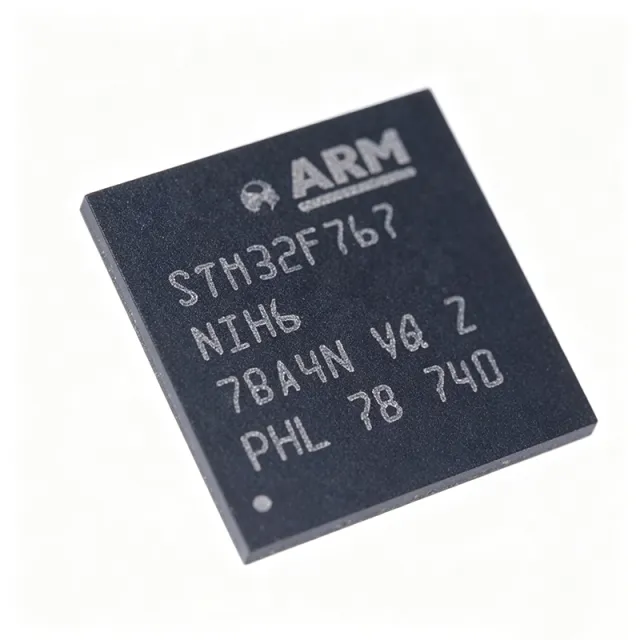
STM32F767NIH6 - 32-bit ARM Cortex-M7 MCU, 2MB Flash, 216MHz | STMicroelectronics
STM32F767NIH6 ✓ ActiveSpecification Comparison
| Parameter | STM32F767BIT6 | STM32F767NIH6 |
|---|---|---|
| Brand | STMicroelectronics | STMicroelectronics |
| Category | Microcontrollers | Microcontrollers |
| Lifecycle Status | Active | Active |
| Stock Status | In Stock | In Stock |
| Unit Price (USD) | $11.85 | $10.85 |
| Core | ARM Cortex-M7 with FPU + DSP instructions | Arm 32-bit Cortex-M7 with double-precision FPU |
| Maximum CPU Clock | 216 MHz | — |
| DMIPS | 462 DMIPS (2.14 DMIPS/MHz, Dhrystone 2.1) | — |
| Program Flash | 2 MB (single-bank, 32-bit fetch) | — |
| SRAM | 384 KB DTCM + 128 KB SRAM + 4 KB backup SRAM | — |
| L1 Cache | 16 KB I-cache + 16 KB D-cache | — |
| ART Accelerator | Yes (0-wait-state execution from Flash) | — |
| Operating Voltage | 1.7 V to 3.6 V | — |
| Package | 208-LQFP (28x28 mm), 0.5 mm pitch | TFBGA-216 (13x13mm, 0.8mm pitch) |
| I/O Pins (max) | 162 GPIOs | — |
| ADC | 3 x 12-bit, up to 2.4 MSPS each | 16-bit, up to 3.6 MSPS |
| DAC | 2 x 12-bit | 12-bit |
| Timers | up to 18 channels incl. 32-bit, IC/OC, PWM | — |
| USB | USB 2.0 OTG FS + HS with integrated HS PHY | — |
| CAN | 2 x CAN 2.0B | — |
| Crypto / Hash | AES-256, SHA-1/2, TRNG (hardware) | — |
| External Memory Bus | SDRAM (up to 32-bit) + SRAM/PSRAM/NOR/NAND | — |
| Display Controller | LCD-TFT, up to 1024x768 + DMA2D | — |
| Octo-SPI / Quad-SPI | 1 x Octo-SPI / 1 x Quad-SPI | — |
| Operating Temperature | -40°C to +85°C (Grade 6) | — |
| Mounting Type | Surface Mount | — |
| MSL Level | 3 (per JEDEC J-STD-020) | — |
| RoHS Status | Compliant | Compliant |
| Maximum Clock Frequency | — | 216 MHz |
| CoreMark / DMIPS | — | 462 DMIPS / 2.14 DMIPS/MHz (Dhrystone 2.1) |
| Cache | — | 16 Kbytes I/D L1-cache |
| Program Memory Size | — | 2 MB Flash (dual-bank) |
| RAM Memory Size | — | 512 KB SRAM |
| Operating Voltage Range | — | 1.7 V to 3.6 V |
| Operating Temperature Range | — | -40 C to +85 C (industrial grade) |
| Number of I/O Lines | — | 159 |
| External Data Bus | — | 32-bit |
| External Address Bus | — | 26-bit |
| I2C Interfaces | — | 4 |
| UART / USART | — | 4 USART + 4 UART |
| SPI Interfaces | — | 6 |
| CAN Interfaces | — | 3 |
| USB Interfaces | — | 2x USB OTG |
| Ethernet | — | 1x 10/100 MAC |
| SDMMC | — | 1x |
| Cryptography | — | AES, DES, 3DES, TRNG |
| Graphics | — | Chrom-ART Accelerator, TFT LCD controller, JPEG codec |
| DSP | — | Yes (DSP instructions) |